MAX2045ETJ+中文资料
General Description
The MAX2045/MAX2046/MAX2047 low-cost, fully inte-grated vector multipliers alter the magnitude and phase of an RF signal. Each device is optimized for the UMTS (MAX2045), DCS/PCS (MAX2046), or cellular/GSM (MAX2047) frequency bands. These devices feature differential RF inputs and outputs.
The MAX2045/MAX2046/MAX2047 provide vector adjustment through the differential I/Q amplifiers. The I/Q amplifiers can interface with voltage and/or current digital-to-analog converters (DACs). The voltage inputs are designed to interface to a voltage-mode DAC, while the current inputs are designed to interface to a current-mode DAC. An internal 2.5V reference voltage is provid-ed for applications using single-ended voltage DACs.The MAX2045/MAX2046/MAX2047 operate from a 4.75V to 5.25V single supply. All devices are offered in a com-pact 5mm ?5mm, 32-lead thin QFN exposed-paddle packages.
The MAX2045/MAX2046/MAX2047 evaluation kits are available, contact factory for availability.
Applications
UMTS/PCS/DCS/Cellular/GSM Base Station
Feed-Forward and Predistortion Power Amplifiers RF Magnitude and Phase Adjustment RF Cancellation Loops Beam-Forming Applications
Features
o Multiple RF Frequency Bands of Operation
2040MHz to 2240MHz (MAX2045)1740MHz to 2060MHz (MAX2046)790MHz to 1005MHz (MAX2047)o ±0.2dB Gain Flatness o ±1°Phase Flatness
o 3dB Control Bandwidth: 260MHz o 15dBm Input IP3
o 15dB Gain Control Range
o Continuous 360°Phase Control Range o 6.5dB Maximum Gain for Continuous Phase o On-Chip Reference for Single-Ended Voltage-Mode Operation o 800mW Power Consumption
o Space-Saving 5mm x 5mm Thin QFN Package o Single 5V supply
MAX2045/MAX2046/MAX2047
High-Gain Vector Multipliers
________________________________________________________________Maxim Integrated Products
1
Ordering Information
19-2728; Rev 0; 1/03
For pricing, delivery, and ordering information,please contact Maxim/Dallas Direct!at 1-888-629-4642, or visit Maxim’s website at https://www.360docs.net/doc/9c4342641.html,.
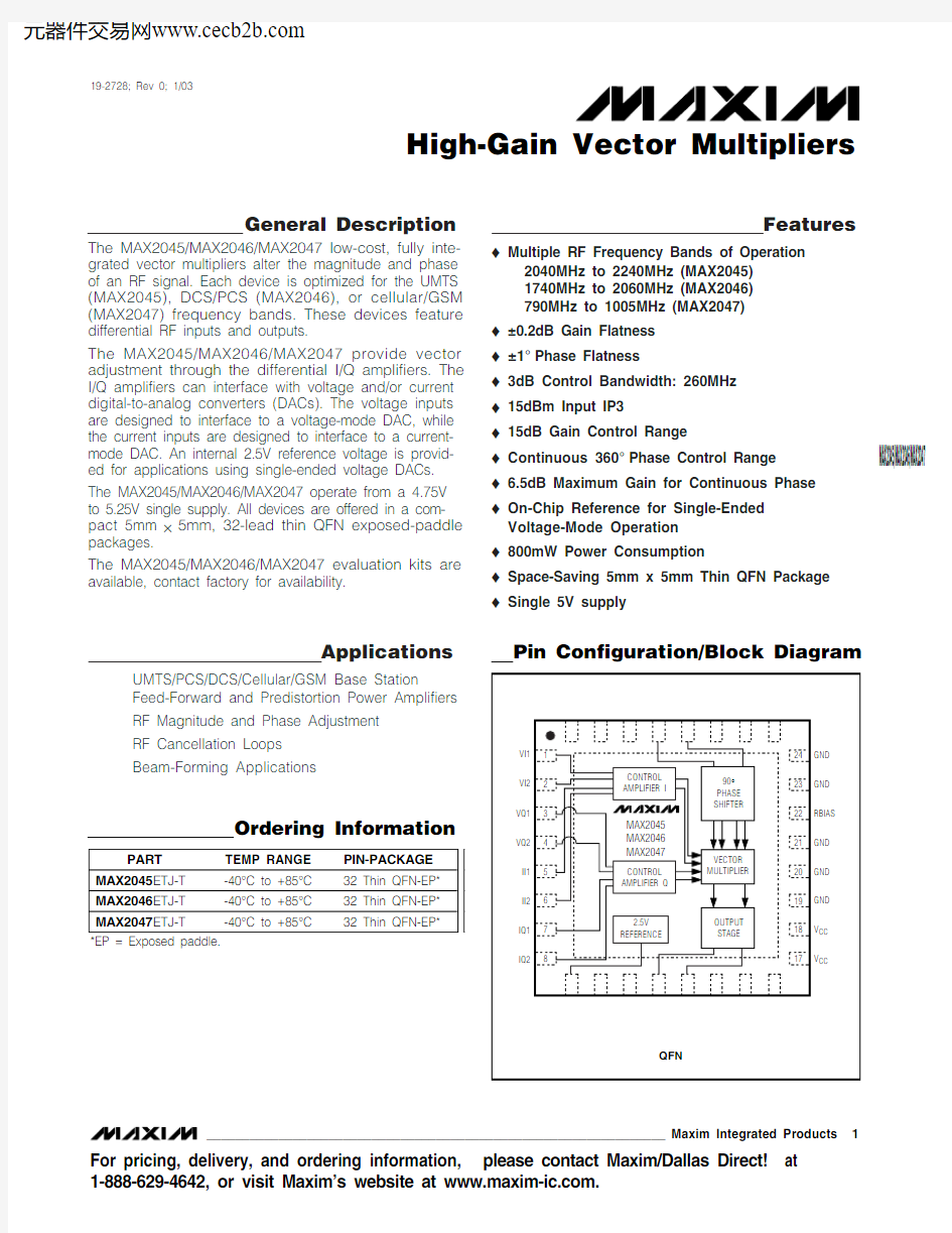
Pin Configuration/Block Diagram
M A X 2045/M A X 2046/M A X 2047
High-Gain Vector Multipliers 2_______________________________________________________________________________________
ABSOLUTE MAXIMUM RATINGS
DC ELECTRICAL CHARACTERISTICS
(Typical Operating Circuit as shown in Figure 1; V CC = 4.75V to 5.25V, T A = -40°C to +85°C, R BIAS = 280?, no RF inputs applied, RF input and output ports are terminated with 50?. Typical values are at V CC = 5V and T A = +25°C, unless otherwise noted.)
Stresses beyond those listed under “Absolute Maximum Ratings” may cause permanent damage to the device. These are stress ratings only, and functional operation of the device at these or any other conditions beyond those indicated in the operational sections of the specifications is not implied. Exposure to absolute maximum rating conditions for extended periods may affect device reliability.
V CC to GND .............................................................-0.3V to +6V VI1, V12, VQ1, VQ2, RFIN1, RFIN2,
RFOUT1, RFOUT2....................................-0.3V to V CC + 0.3V RFOUT1, RFOUT2 Sink Current..........................................35mA REFOUT Source Current.......................................................4mA II1, II2, IQ1, IQ2........................................................-0.3V to +1V II1, II2, IQ1, IQ2 Sink Current ...........................................+10mA
Continuous RF Input Power (CW)...................................+15dBm Continuous Power Dissipation (T A = +70°C)
32-Pin Thin QFN (derate 21.3mW/°C above +70°C).......1.7W Operating Temperature Range ...........................-40°C to +85°C Junction Temperature......................................................+150°C Storage Temperature Range.............................-40°C to +150°C Lead Temperature (soldering, 10s).................................+300°C
AC ELECTRICAL CHARACTERISTICS
(Typical Operating Circuit as shown in Figure 1; V CC = 4.75V to 5.25V, T A = -40°C to +85°C, R BIAS = 280?, f IN = 2.14GH z (MAX2045), f IN = 1.9GHz (MAX2046), f IN = 915MHz (MAX2047), input current range = 0 to 4mA (if using a current-mode DAC), and differential input voltage range = 0 to 0.707V (if using a voltage-mode DAC). If using a current-mode DAC, voltage mode I/Q inputs
MAX2045/MAX2046/MAX2047
High-Gain Vector Multipliers
_______________________________________________________________________________________3
MAX2045 ELECTRICAL CHARACTERISTICS
(Typical Operating Circuit as shown in Figure 1; V CC = 4.75V to 5.25V, T A = -40°C to +85°C, R BIAS = 280?, f IN = 2.14GHz, input cur-rent range = 0 to 4mA (if using a current-mode DAC), and differential input voltage range = 0 to 0.707V (if using a voltage-mode DAC). If using a current-mode DAC, voltage mode I/Q inputs are left open. If using a voltage-mode DAC, all current-mode I/Q inputs
M A X 2045/M A X 2046/M A X 2047
High-Gain Vector Multipliers
MAX2046 ELECTRICAL CHARACTERISTICS
(Typical Operating Circuit as shown in Figure 1; V CC = 4.75V to 5.25V, T A = -40°C to +85°C, R BIAS = 280?, f IN = 1.9GHz, input cur-rent range = 0 to 4mA (if using a current-mode DAC), and differential input voltage range = 0 to 0.707V (if using a voltage-mode DAC). If using a current-mode DAC, voltage mode I/Q inputs are left open. If using a voltage-mode DAC, all current-mode I/Q inputs are left open. Typical values are at V CC = 5V and T A = +25°C, unless otherwise noted.) (Notes 1, 2, 3)
MAX2045 ELECTRICAL CHARACTERISTICS (continued)
(Typical Operating Circuit as shown in Figure 1; V CC = 4.75V to 5.25V, T A = -40°C to +85°C, R BIAS = 280?, f IN = 2.14GHz, input cur-rent range = 0 to 4mA (if using a current-mode DAC), and differential input voltage range = 0 to 0.707V (if using a voltage-mode DAC). If using a current-mode DAC, voltage mode I/Q inputs are left open. If using a voltage-mode DAC, all current-mode I/Q inputs are left open. Typical values are at V CC = 5V and T A = +25°C, unless otherwise noted.) (Notes 1, 2, 3)
MAX2045/MAX2046/MAX2047
High-Gain Vector Multipliers
_______________________________________________________________________________________5
MAX2046 ELECTRICAL CHARACTERISTICS (continued)
(Typical Operating Circuit as shown in Figure 1; V CC = 4.75V to 5.25V, T A = -40°C to +85°C, R BIAS = 280?, f IN = 1.9GHz, input cur-rent range = 0 to 4mA (if using a current-mode DAC), and differential input voltage range = 0 to 0.707V (if using a voltage-mode DAC). If using a current-mode DAC, voltage mode I/Q inputs are left open. If using a voltage-mode DAC, all current-mode I/Q inputs are left open. Typical values are at V CC = 5V and T A = +25°C, unless otherwise noted.) (Notes 1, 2, 3)
M A X 2045/M A X 2046/M A X 2047
High-Gain Vector Multipliers 6_______________________________________________________________________________________
MAX2047 ELECTRICAL CHARACTERISTICS
(Typical Operating Circuit as shown in Figure 1; V CC = 4.75V to 5.25V, T A = -40°C to +85°C, R BIAS = 280?, f IN = 915MHz, input cur-rent range = 0 to 4mA (if using a current-mode DAC), and differential input voltage range = 0 to 0.707V (if using a voltage-mode DAC). If using a current-mode DAC, voltage mode I/Q inputs are left open. If using a voltage-mode DAC, all current-mode I/Q inputs
MAX2045/MAX2046/MAX2047
High-Gain Vector Multipliers
_______________________________________________________________________________________7
Note 1:Guaranteed by design and characterization.
Note 2:All specifications reflect losses and delays of external components (matching components, baluns, and PC board traces).
Output measurements taken at the RF OUTPUT of the Typical Operating Circuit .
Note 3:Radius is defined as (VI 2+ VQ 2)0.5. VI denotes the difference between VI1 and VI2. VQ denotes the difference between VQ1
and VQ2. For differential operation: VI1 = V REF + 0.5 ?VI, VI2 = V REF - 0.5 ?VI, VQ1 = V REF + 0.5 ?VQ, VQ2 = V REF - 0.5 ?VQ. For single-ended operation: VI1 = V REF + VI, VI2 = V REF , VQ1 = V REF + VQ, VQ2 = V REF .
Note 4:When using the I/Q current inputs, maximum gain occurs when one differential input current is zero and the other corre-sponding differential input is 5mA. Minimum gain occurs when both differential inputs are equal.
MAX2047 ELECTRICAL CHARACTERISTICS (continued)
(Typical Operating Circuit as shown in Figure 1; V CC = 4.75V to 5.25V, T A = -40°C to +85°C, R BIAS = 280?, f IN = 915MHz, input cur-rent range = 0 to 4mA (if using a current-mode DAC), and differential input voltage range = 0 to 0.707V (if using a voltage-mode DAC). If using a current-mode DAC, voltage mode I/Q inputs are left open. If using a voltage-mode DAC, all current-mode I/Q inputs
M A X 2045/M A X 2046/M A X 2047
High-Gain Vector Multipliers 8_______________________________________________________________________________________
Typical Operating Characteristics (MAX2045)
(V CC = 5V, f IN = 2140MHz, V_1 = VI1 and VQ1, V_2 = VI2 and VQ2, I_1 = II1 and IQ1, I_2 = II2 and IQ2, VI1 = VQ1 = 3.2V, VI2 =VQ2 = REFOUT, P IN = -15dBm per tone at 1MHz offset (IIP3), and T A = +25°C, unless otherwise noted.)
REFOUT AND SUPPLY CURRENT
vs. TEMPERATURE AND SUPPLY VOLTAGE
TEMPERATURE (°C)
S U P P L Y C U R R E N T (m A )
60
35
10
-15
150160170180190200210220230140
R E F O U T (V )
2.462.452.442.472.482.492.502.51
2.52
2.43
-40
85
INPUT RETURN LOSS vs. FREQUENCY
FREQUENCY (MHz)I N P U T R E T U R N L O S S (d B )
225022002150210020501918171615141312111020
20002300OUTPUT RETURN LOSS vs. FREQUENCY
FREQUENCY (MHz)
O U T P U T R E T U R N L O S S (d B )
225022002150210020501918171615141312
202122
20002300
GAIN vs. FREQUENCY
FREQUENCY (MHz)G A I N (d B )
2250
2200
2150
2100
2050
-15-10-505101520-20-25-30
2000
2300
GAIN vs. FREQUENCY
FREQUENCY (MHz)G A I N (d B )
2250
2200
2150
2100
2050
-15-10-505
1015-20
-25-30
2000
2300
GAIN vs. CONTROL VOLTAGE (VI1 = VQ1)
CONTROL VOLTAGE VI1, VQ1 (V)
G A I N (d B )
3.75
3.50
3.25
3.00
2.75
-25-20
-15-10-505
1015
-302.50
4.00
GAIN vs. CONTROL VOLTAGE (VI1 = VQ1)
CONTROL VOLTAGE VI1, VQ1 (V)G A I N (d B )
3.753.503.253.002.75-45-40-35-30-25-20-15-10-505101520-502.50
4.00
REVERSE ISOLATION vs. FREQUENCY
FREQUENCY (MHz)I S O L A T I O N (d B )
2250220021502100205011010090807060504030120
2000
2300OUTPUT NOISE POWER vs. FREQUENCY
FREQUENCY (MHz)
O U T P U T N O I S E P O W E R (d B m /H z )22502200215021002050-148.5-148.0-147.5-147.0-146.5-146.0-145.5-145.0-144.5-144.0
-149.0
20002300
MAX2045/MAX2046/MAX2047
High-Gain Vector Multipliers
_______________________________________________________________________________________9
OUTPUT NOISE POWER
vs. CONTROL VOLTAGE (VI1 = VQ1)
CONTROL VOLTAGE VI1, VQ1 (V)O U T P U T N O I S E P O W E R (d B m /H z ) 3.75
3.50
3.25
3.00
2.75
-148.5-148.0-147.5-147.0-146.5-146.0-145.5-145.0-144.5-144.0-149.0
2.50
4.00
OUTPUT NOISE POWER
vs. CONTROL VOLTAGE (VI1 = VQ1)
CONTROL VOLTAGE VI1, VQ1 (V)
O U T P U T N O I S E P O W E R (d B m /H z ) 3.75
3.50
3.25
3.00
2.75
-148.5-148.0-147.5-147.0-146.5-146.0-145.5-145.0-144.5-144.0-149.0
2.50
4.00
INPUT P1-dB COMPRESSION
vs. FREQUENCY
FREQUENCY (MHz)
I N P U T P 1-d B (d B m )
2250
2200
2050
2100
2150
5.5
6.0
6.5
7.07.5
8.08.5
9.0
5.02000
2300
INPUT P1-dB COMPRESSION
vs. FREQUENCY
FREQUENCY (MHz)I N P U T P 1-d B (d B m )
225022002050210021505.56.06.57.07.58.08.59.05.0
20002300
INPUT P1-dB COMPRESSION vs. CONTROL VOLTAGE (VI1 = VQ1)
CONTROL VOLTAGE VI1, VQ1 (V)
I N P U T P 1-d B (d B m )
3.75
3.50
3.25
3.00
2.75
6789101112131415165
2.50
4.00
INPUT P1-dB COMPRESSION vs. CONTROL VOLTAGE (VI1 = VQ1)
CONTROL VOLTAGE VI1, VQ1 (V)
I N P U T P 1-d B (d B m )
3.75
3.50
3.25
3.00
2.75
678910111213141516
5
2.50
4.00
IIP3 vs. FREQUENCY
FREQUENCY (MHz)I I P 3 (d B m )
225022002150
2100
2050
13.514.014.515.015.516.013.0
2000
2300IIP3 vs. FREQUENCY
FREQUENCY (MHz)I I P 3 (d B m )
2250220021502100205013.514.014.515.015.516.0
13.0
20002300
IIP3 vs. CONTROL VOLTAGE (VI1 = VQ1)
CONTROL VOLTAGE VI1 , VQ1, (V)
I I P 3 (d B m )
3.753.503.253.002.7567891011121314151617181952.50
4.00
Typical Operating Characteristics (MAX2045) (continued)
(V CC = 5V, f IN = 2140MHz, V_1 = VI1 and VQ1, V_2 = VI2 and VQ2, I_1 = II1 and IQ1, I_2 = II2 and IQ2, VI1 = VQ1 = 3.2V, VI2 =VQ2 = REFOUT, P IN = -15dBm per tone at 1MHz offset (IIP3), and T A = +25°C, unless otherwise noted.)
M A X 2045/M A X 2046/M A X 2047
High-Gain Vector Multipliers 10______________________________________________________________________________________
IIP3 vs. CONTROL VOLTAGE (VI1 = VQ1)
CONTROL VOLTAGE VI1 , VQ1, (V)
I I P 3 (d B m )
3.753.503.253.002.7567891011121314151617181952.50
4.00
GAIN vs. PHASE
PHASE (DEGREES)
G A I N (d B )
31527018022590
13545
-14-12-10-8-6-4-20246810-16
360
S21 PHASE vs. FREQUENCY
FREQUENCY (MHz)
P H A S E (D E G R E E S )
22502200215021002050
80.581.081.582.082.583.083.584.084.585.085.586.0
80.0
2000
2300
S21 PHASE vs. FREQUENCY
FREQUENCY (MHz)P H A S E (D E G R E E S )
2250
2200
2150
2100
2050
74.575.075.576.076.577.077.578.078.579.079.580.074.0
2000
2300
S21 PHASE vs. FREQUENCY
FREQUENCY (MHz)P H A S E (D E G R E E S )
2250
2200
2150
2100
2050
7075
8085909510065
2000
2300
S21 PHASE vs. FREQUENCY
FREQUENCY (MHz)
P H A S E (D E G R E E S )
2250
2200
2150
2100
2050
65
7075808590602000
2300
GROUP DELAY vs. FREQUENCY
FREQUENCY (MHz)
G R O U P D E L A Y (n s )
225022002150210020501.101.051.151.201.251.301.351.401.501.451.551.601.651.751.701.801.851.901.00
20002300
SWITCHING SPEED
SWITCHING SPEED (1ns/div)
D I F F
E R E N T I A L C O N T R O L S I G N A L
G A I N
Typical Operating Characteristics (MAX2045) (continued)
(V CC = 5V, f IN = 2140MHz, V_1 = VI1 and VQ1, V_2 = VI2 and VQ2, I_1 = II1 and IQ1, I_2 = II2 and IQ2, VI1 = VQ1 = 3.2V, VI2 =VQ2 = REFOUT, P IN = -15dBm per tone at 1MHz offset (IIP3), and T A = +25°C, unless otherwise noted.)
MAX2045/MAX2046/MAX2047
High-Gain Vector Multipliers
______________________________________________________________________________________11
REFOUT AND SUPPLY CURRENT
vs. TEMPERATURE AND SUPPLY VOLTAGE
TEMPERATURE (°C)
S U P P L Y C U R R E N T (m A )
60
35
10
-15
150160170180190200210220140
R E F O U T (V )2.452.462.472.482.492.50
2.51
2.522.44
-40
85
INPUT RETURN LOSS vs. FREQUENCY
FREQUENCY (MHz)
I N P U T R E T U R N L O S S (d B )
200020501950185019001800
17502220181614121024
17002100
OUTPUT RETURN LOSS vs. FREQUENCY
FREQUENCY (MHz)
O U T P U T R E T U R N L O S S (d B )
20502000195018501900180017501918171615141312
202122
17002100
GAIN vs. FREQUENCY
FREQUENCY (MHz)
G A I N (d B )
2050200019501900185018001750-15-10-505101520-20-25-30
17002100
GAIN vs. FREQUENCY
FREQUENCY (MHz)
G A I N (d B )
2050200019501850190018001750-15-10-5051015-20
-25-30
1700
2100
GAIN vs. CONTROL VOLTAGE (VI1 = VQ1)
CONTROL VOLTAGE VI1, VQ1 (V)
G A I N (d B )
3.75
3.50
3.25
3.00
2.75
-25-20-15
-10-505
1020
15-302.50
4.00
GAIN vs. CONTROL VOLTAGE (VI1 = VQ1)
CONTROL VOLTAGE VI1, VQ1 (V)
G A I N (d B )
3.753.503.253.002.75-45-40-35-30-25-20-15-10-505101520-502.50
4.00
REVERSE ISOLATION vs. FREQUENCY
FREQUENCY (MHz)
I S O L A T I O N (d B )
205020001950190018501800175011010090807060504030120
17002100
OUTPUT NOISE POWER vs. FREQUENCY
FREQUENCY (MHz)
O U T P U T N O I S E P O W E R (d B m /H z )2050200019501900185017501800-148.5-148.0-147.5-147.0-146.5-146.0-145.5-145.0-144.5-144.0
-149.0
17002100
Typical Operating Characteristics (MAX2046)
(V CC = 5V, f IN = 1900MHz, V_1 = VI1 and VQ1, V_2 = VI2 and VQ2, I_1 = II1 and IQ1, I_2 = II2 and IQ2, VI1 = VQ1 = 3.2V, VI2 =VQ2 = REFOUT, P IN = -15dBm per tone at 1MHz offset (IIP3), and T A = +25°C, unless otherwise noted.)
M A X 2045/M A X 2046/M A X 2047
High-Gain Vector Multipliers 12______________________________________________________________________________________
OUTPUT NOISE POWER
vs. CONTROL VOLTAGE (VI1 = VQ1)
CONTROL VOLTAGE VI1, VQ1 (V)
O U T P U T N O I S E P O W E R (d B m /H z ) 3.753.503.253.002.75-148.5-148.0-147.5-147.0-146.5-146.0-145.5-145.0-144.5-144.0-149.0
2.50 4.00
INPUT P1-dB COMPRESSION
vs. FREQUENCY
FREQUENCY (MHz)
I N P U T P 1-d B (d B m )
20502000195017501800190018505.5
6.06.5
7.07.5
8.08.5
9.0
5.0
17002100
INPUT P1-dB COMPRESSION
vs. FREQUENCY
FREQUENCY (MHz)
I N P U T P 1-d B (d B m )
20502000175018001900195018505.56.06.57.07.58.08.59.05.0
17002100
INPUT P1-dB COMPRESSION vs. CONTROL VOLTAGE (VI1 = VQ1)
CONTROL VOLTAGE VI1, VQ1 (V)
I N P U T P 1-d B (d B m )
3.75
3.50
3.25
3.00
2.75
6789101112131415165
2.50
4.00
INPUT P1-dB COMPRESSION vs. CONTROL VOLTAGE (VI1 = VQ1)
CONTROL VOLTAGE VI1, VQ1 (V)
I N P U T P 1-d B (d B m )
3.75
3.50
3.25
3.00
2.75
67
8910111213141516
5
2.50
4.00
IIP3 vs. FREQUENCY
FREQUENCY (MHz)
I I P 3 (d B m )
2000190018501800175013.514.014.515.016.015.517.016.513.0
17002100
19502050IIP3 vs. FREQUENCY
FREQUENCY (MHz)
I I P 3 (d B m )
2000190018501800175013.514.014.5
15.015.517.016.516.0
13.0
17002100
19502050
IIP3 vs. CONTROL VOLTAGE (VI1 = VQ1)
CONTROL VOLTAGE VI1 , VQ1, (V)
I I P 3 (d B m )
3.753.503.253.002.75
67891011121314151617181952.50
4.00
Typical Operating Characteristics (MAX2046) (continued)
(V CC = 5V, f IN = 1900MHz, V_1 = VI1 and VQ1, V_2 = VI2 and VQ2, I_1 = II1 and IQ1, I_2 = II2 and IQ2, VI1 = VQ1 = 3.2V, VI2 =VQ2 = REFOUT, P IN = -15dBm per tone at 1MHz offset (IIP3), and T A = +25°C, unless otherwise noted.)
OUTPUT NOISE POWER
vs. CONTROL VOLTAGE (VI1 = VQ1)
CONTROL VOLTAGE VI1, VQ1 (V)O U T P U T N O I S E P O W E R (d B m /H z ) 3.75
3.50
3.25
3.00
2.75
-148.5-148.0-147.5-147.0-146.5-146.0-145.5-145.0-144.5-144.0-149.0
2.50
4.00
MAX2045/MAX2046/MAX2047
High-Gain Vector Multipliers
______________________________________________________________________________________13
IIP3 vs. CONTROL VOLTAGE (VI1 = VQ1)
CONTROL VOLTAGE VI1 , VQ1, (V)
I I P 3 (d B m )
3.753.503.253.002.75
67891011121314151617181952.50
4.00
GAIN vs. PHASE
PHASE (DEGREES)
G A I N (d B )
31527018022590
13545
-14-12-10-8-6-4-20246810-16
360
S21 PHASE vs. FREQUENCY
FREQUENCY (MHz)
P H A S E (D E G R E E S )
2050200019501900185018001750-154-153-152-151-150-149-148-147-146-145-144-143-142-141-140-155
17002100
S21 PHASE vs. FREQUENCY
FREQUENCY (MHz)
P H A S E (D E G R E E S )
2050200019501900185018001750-169-168-167-166-165-164-163-162-161-160-159-158-157-156-155-170
17002100
S21 PHASE vs. FREQUENCY
FREQUENCY (MHz)
P H A S E (D E G R E E S )
200019501900185018001750-180-185-175-170-165-160-155-150-145-140-135-130-190
17002100
2050
S21 PHASE vs. FREQUENCY
FREQUENCY (MHz)
P H A S E (D E G R E E S )
20001900185018001750-180-185-170-175-155-160-165-150-135-140-145-130-190
17002100
19502050GROUP DELAY vs. FREQUENCY
FREQUENCY (MHz)
G R O U P D E L A Y (n s )
200019001850180017501.351.401.451.501.551.601.651.701.751.801.851.901.30
17002100
19502050SWITCHING SPEED
SWITCHING SPEED (1ns/div)
D I F F
E R E N T I A L C O N T R O L S I G N A L
G A I N
Typical Operating Characteristics (MAX2046) (continued)
(V CC = 5V, f IN = 1900MHz, V_1 = VI1 and VQ1, V_2 = VI2 and VQ2, I_1 = II1 and IQ1, I_2 = II2 and IQ2, VI1 = VQ1 = 3.2V, VI2 =VQ2 = REFOUT, P IN = -15dBm per tone at 1MHz offset (IIP3), and T A = +25°C, unless otherwise noted.)
M A X 2045/M A X 2046/M A X 2047
High-Gain Vector Multipliers 14______________________________________________________________________________________
OUTPUT RETURN LOSS vs. FREQUENCY
FREQUENCY (MHz)
O U T P U T R E T U R N L O S S (d B )
10501000950850900800750141312111098
1516
7001100
GAIN vs. FREQUENCY
FREQUENCY (MHz)
G A I N (d B )
10501000950900850800750-15
-10-505
101520-20
7001100
GAIN vs. FREQUENCY
FREQUENCY (MHz)
G A I N (d B )
10501000950850900800750-15-10
-5051015-20
7001100
GAIN vs. CONTROL VOLTAGE (VI1 = VQ1)
CONTROL VOLTAGE VI1, VQ1 (V)
G A I N (d B )
3.75
3.50
3.25
3.00
2.75
-25-20
-15-10-505
1020
15-302.50
4.00
GAIN vs. CONTROL VOLTAGE (VI1 = VQ1)
CONTROL VOLTAGE VI1, VQ1 (V)
G A I N (d B )
3.75
3.50
3.25
3.00
2.75
-35-30-25-20-15-10-5051015202.50
4.00
REVERSE ISOLATION vs. FREQUENCY
FREQUENCY (MHz)
I S O L A T I O N (d B )
10501000950900850800750110
10090807060504030
120
7001100
OUTPUT NOISE POWER vs. FREQUENCY
FREQUENCY (MHz)
O U T P U T N O I S E P O W E R (d B m /H z )
1000900850800750-150-149-148-147-146-145-144-151
7001100
9501050
Typical Operating Characteristics (MAX2047)
(V CC = 5V, f IN = 915MHz, V_1 = VI1 and VQ1, V_2 = VI2 and VQ2, I_1 = II1 and IQ1, I_2 = II2 and IQ2, VI1 = VQ1 = 3.2V, VI2 = VQ2= REFOUT, P IN = -15dBm per tone at 1MHz offset (IIP3), and T A = +25°C, unless otherwise noted.)
REFOUT AND SUPPLY CURRENT
vs. TEMPERATURE AND SUPPLY VOLTAGE
TEMPERATURE (°C)
S U P P L Y C U R R E N T (m A )
60
35
10
-15
150
160170180190200210140
R E F O U T (V )
2.462.472.482.49
2.502.51
2.522.45
-40
85
INPUT RETURN LOSS vs. FREQUENCY
FREQUENCY (MHz)
I N P U T R E T U R N L O S S (d B )
100010509508509008007502220181614121032
242628307001100
MAX2045/MAX2046/MAX2047
High-Gain Vector Multipliers
______________________________________________________________________________________15
INPUT P1-dB COMPRESSION
vs. FREQUENCY
FREQUENCY (MHz)
I N P U T P 1-d B (d B m )
105010009507508009008505.5
6.0
6.5
7.07.5
8.08.5
9.0
5.0
7001100
INPUT P1-dB COMPRESSION
vs. FREQUENCY
FREQUENCY (MHz)
I N P U T P 1-d B (d B m )
105010007508009009508505.56.06.57.07.58.08.59.05.0
7001100
INPUT P1-dB COMPRESSION vs. CONTROL VOLTAGE (VI1 = VQ1)
CONTROL VOLTAGE VI1, VQ1 (V)I N P U T P 1-d B (d B m )
3.753.503.253.002.75
4.5
5.05.5
6.06.5
7.07.5
8.08.5
9.09.510.04.02.50
4.00
INPUT P1-dB COMPRESSION vs. CONTROL VOLTAGE (VI1 = VQ1)
CONTROL VOLTAGE VI1, VQ1 (V)
I N P U T P 1-d B (d B m )
3.753.503.253.002.75
4.0
4.5
5.05.5
6.06.5
7.07.5
8.08.5
9.0
2.50 4.00
IIP3 vs. FREQUENCY
FREQUENCY (MHz)
I I P 3 (d B m )
100090085080075014.515.515.016.016.517.018.017.519.018.514.0
7001100
9501050
IIP3 vs. CONTROL VOLTAGE (VI1 = VQ1)
CONTROL VOLTAGE VI1 , VQ1 (V)
I I P 3 (d B m )
3.753.503.253.002.75
789101112131415161718192.50
4.00
Typical Operating Characteristics (MAX2047) (continued)
(V CC = 5V, f IN = 915MHz, V_1 = VI1 and VQ1, V_2 = VI2 and VQ2, I_1 = II1 and IQ1, I_2 = II2 and IQ2, VI1 = VQ1 = 3.2V, VI2 = VQ2= REFOUT, P IN = -15dBm per tone at 1MHz offset (IIP3), and T
A = +25°C, unless otherwise noted.)
IIP3 vs. FREQUENCY
FREQUENCY (MHz)
I I P 3 (d B m )
100090085080075015.015.5
16.0
16.517.018.518.017.514.5
7001100
9501050OUTPUT NOISE POWER
vs. CONTROL VOLTAGE (VI1 = VQ1)
CONTROL VOLTAGE VI1, VQ1 (V)O U T P U T N O I S E P O W E R (d B m /H z ) 3.75
3.50
3.25
3.00
2.75
-148.5-148.0-147.5-147.0-146.5-146.0-145.5-145.0-149.0-149.5-150.0
2.50
4.00OUTPUT NOISE POWER
vs. CONTROL VOLTAGE (VI1 = VQ1)
CONTROL VOLTAGE VI1, VQ1 (V)
O U T P U T N O I S E P O W E R (d B m /H z ) 3.75
3.50
3.253.002.75-148.5-148.0-147.5-147.0-146.5-146.0-145.5-145.0-149.0-149.5-150.0
2.50 4.00
M A X 2045/M A X 2046/M A X 2047
High-Gain Vector Multipliers 16______________________________________________________________________________________
S21 PHASE vs. FREQUENCY
FREQUENCY (MHz)
P H A S E (D E G R E E S )
10501000950900850800750115120125130135140145150
110
7001100
S21 PHASE vs. FREQUENCY
FREQUENCY (MHz)
P H A S E (D E G R E E S )
10501000950900850800750105110115120125130135140145150100
7001100
S21 PHASE vs. FREQUENCY
FREQUENCY (MHz)
P H A S E (D E G R E E S )
1000950900850800750110
120130
140
150160100
7001100
1050
S21 PHASE vs. FREQUENCY
FREQUENCY (MHz)
P H A S E (D E G R E E S )
1000900850800750110
10012015014013016090
7001100
9501050
GROUP DELAY vs. FREQUENCY
FREQUENCY (MHz)G R O U P D E L A Y (n s )
10009008508007501.6
1.71.81.9
2.0
2.12.22.32.42.52.62.7
7001100
9501050SWITCHING SPEED
SWITCHING SPEED (1ns/div)
D I F F
E R E N T I A L C O N T R O L S I G N A L
G A I
N
Typical Operating Characteristics (MAX2047) (continued)
(V CC = 5V, f IN = 915MHz, V_1 = VI1 and VQ1, V_2 = VI2 and VQ2, I_1 = II1 and IQ1, I_2 = II2 and IQ2, VI1 = VQ1 = 3.2V, VI2 = VQ2= REFOUT, P IN = -15dBm per tone at 1MHz offset (IIP3), and T A = +25°C, unless otherwise noted.)
IIP3 vs. CONTROL VOLTAGE (VI1 = VQ1)
CONTROL VOLTAGE VI1 , VQ1 (V)
I I P 3 (d B m )
3.753.503.253.002.757891011121314151617181920212.50
4.00
GAIN vs. PHASE
PHASE (DEGREES)
G A I N (d B )
31527018022590
13545
-13-11-9-7-5-3-11357911-15
360
Detailed Description The MAX2045/MAX2046/MAX2047 provide vector adjustment through the differential I/Q amplifiers. Each part is optimized for separate frequency ranges: MAX2045 for f IN= 2040MHz to 2240MHz, MAX2046 for f IN= 1740MH z to 2060MH z, and MAX2047 for f IN= 790MH z to 1005MH z. All three devices can be inter-faced using current- and/or voltage-mode DACs.
The MAX2045/MAX2046/MAX2047 accept differential RF inputs, which are internally phase shifted 90 degrees to produce differential I/Q signals. The phase and magnitude of each signal can then be adjusted using the voltage- and/or current-control inputs. Figure 1 shows a typical operating circuit when using both current- and voltage-mode DACs. When using only one of the two, leave the unused I/Q inputs open.The RF input and output ports require external matching
for optimal performance. See Figures 1 and 2 for appro-
priate component values. The output ports require external biasing. In Figures 1 and 2, the outputs are biased through the balun (T2). The RF input ports can
be driven differentially or single ended (Figures 1, 2)
using a balun.The matching values for the MAX2045/
MAX2046 were set to be the same during characteriza-
tion. An optimized set of values can be found in the
MAX2045/MAX2046/MAX2047 Evaluation Kit data sheet.
I/Q Inputs
The control amplifiers convert a voltage, current, or voltage and current input to a predistorted voltage that controls the multipliers. The I/Q voltage-mode inputs
can be operated differentially (Figure 1) or single ended (Figure 2). A 2.5V reference is provided on-chip
for single-ended operation. MAX2045/MAX2046/MAX2047
High-Gain Vector Multipliers ______________________________________________________________________________________17
M A X 2045/M A X 2046/M A X 2047
High-Gain Vector Multipliers 18______________________________________________________________________________________
Figure 1. Typical Operating Circuit Using Differential Current- and Voltage-Mode DACs
MAX2045/MAX2046/MAX2047
High-Gain Vector Multipliers
______________________________________________________________________________________
19
Figure 2. Typical Operating Circuit Using Single-Ended Voltage Mode DACs
M A X 2045/M A X 2046/M A X 2047
On-Chip Reference Voltage
An on-chip, 2.5V reference voltage is provided for single-ended control mode. Connect REFOUT to VI2and VQ2 to provide a stable reference voltage. The equivalent output resistance of the REFOUT pin is approximately 80?. REFOUT is capable of sourcing 1mA of current, with <10mV drop-in voltage.
Applications Information
RF Single-Ended Operation
The RF input impedance is 50?differential into the IC.An external low-loss 1:1 balun can be used for single-ended operation. The RF output impedance is 300?differential into the IC. An external low-loss 4:1 balun transforms this impedance down to 50?single-ended output (Figures 1 and 2).
Bias Resistor
The bias resistor value (280?) was optimized during characterization at the factory. This value should not be adjusted. If the 280?(±1%) resistor is not readily avail-able, substitute a standard 280?(±5%) resistor, which may result in more current part-to-part variation.
Switching Speed
The control inputs have a typical 3dB BW of 260MH z.This BW provides the device with the ability to adjust gain/phase at a very rapid rate. The Switching Speed graphs in the Typical Operating Characteristics try to capture the control ability of the vector multipliers.These measurements were done by first removing capacitors C4–C7 to reduce driving capacitance.
The test for gathering the curves shown, uses a MAX9602 differential output comparator to drive VI1,VI2, VQ1, and VQ2. One output of the comparator is connected to VI1/VQ1, while the other is connected to VI2/VQ2. The input to the vector multiplier is driven by an RF source and the output is connected to a crystal detector. The switching signal produces a waveform that results in a ±0.7V differential input signal to the vector multiplier.
This signal switches the signal from quadrant 3 (-0.7V case), through the origin (maximum attenuation), and into quadrant 1 (+0.7V case). The before-and-after amplitude (S21) stays about the same between the two quadrants but the phase changes by 180°.
As the differential control signal approaches zero, the gain approaches its minimum value. This appears as the null in the Typical Operating Characteristics . The measurement results include rise-time errors from the crystal detector (specified by manufacturing to be approximately 8ns to 12ns), the comparator (approxi-mately 500ps), and the 500MHz BW oscilloscope (used to measure the control and detector signals).
Layout Issues
A properly designed PC board is an essential part of any RF/microwave circuit. Keep RF signal lines as short as possible to reduce losses, radiation, and inductance.For best performance, route the ground pin traces directly to the exposed pad underneath the package.This pad should be connected to the ground plane of the board by using multiple vias under the device to provide the best RF/thermal conduction path. Solder the exposed pad on the bottom of the device package to a PC board exposed pad.
The MAX2045/MAX2046/MAX2047 Evaluation Kit can be used as a reference for board layout. Gerber files are available upon request at https://www.360docs.net/doc/9c4342641.html,.
Power-Supply Bypassing
Proper voltage-supply bypassing is essential for high-frequency circuit stability. Bypass the V CC pins with 10nF and 22pF (47pF for the MAX2047) capacitors.Connect the high-frequency capacitor as close to the device as possible.
Exposed Paddle RF Thermal
Considerations
The EP of the 32-lead thin QFN package provides a low thermal-resistance path to the die. It is important that the PC board on which the IC is mounted be designed to conduct heat from this contact. In addition, the EP provides a low-inductance RF ground path for the device.It is recommended that the EP be soldered to a ground plane on the PC board, either directly or through an array of plated via holes.
Soldering the pad to ground is also critical for proper heat dissipation. Use a solid ground plane wherever possible.
Chip Information
TRANSISTOR COUNT: 599
High-Gain Vector Multipliers 20______________________________________________________________________________________