CE8301-EN-22
Small Package PFM Control
Step-Up DC/DC Converter CE8301 Series
INTRODUCTION
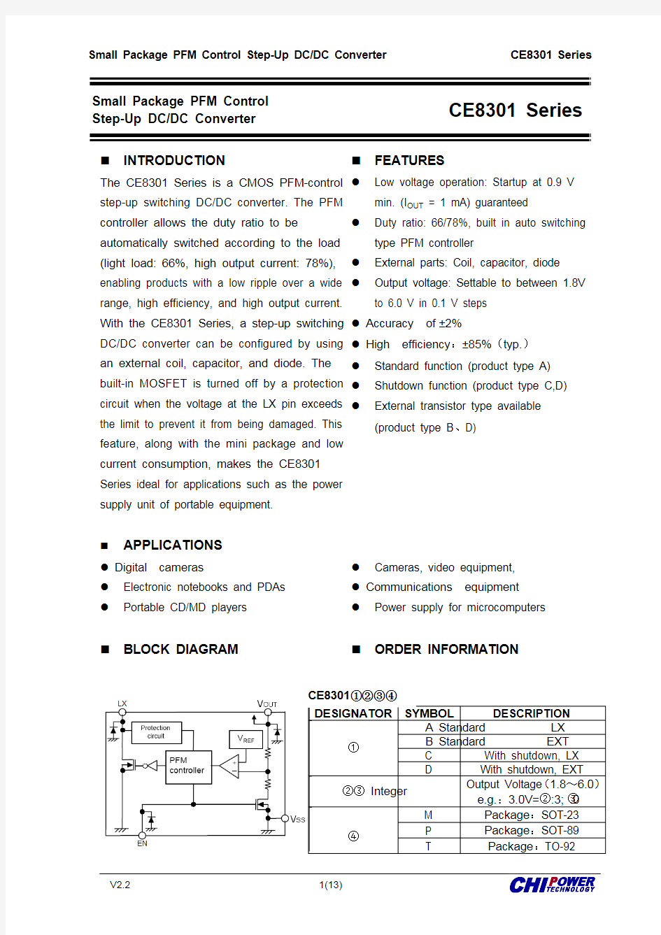
The CE8301 Series is a CMOS PFM-control step-up switching DC/DC converter. The PFM controller allows the duty ratio to be automatically switched according to the load
(light load: 66%, high output current: 78%), enabling products with a low ripple over a wide range, high efficiency, and high output current.
With the CE8301 Series, a step-up switching DC/DC converter can be configured by using an external coil, capacitor, and diode. The built-in MOSFET is turned off by a protection circuit when the voltage at the LX pin exceeds the limit to prevent it from being damaged. This feature, along with the mini package and low current consumption, makes the CE8301 Series ideal for applications such as the power supply unit of portable equipment. FEATURES
z Low voltage operation: Startup at 0.9 V min. (I OUT = 1 mA) guaranteed z Duty ratio: 66/78%, built in auto switching type PFM controller
z External parts: Coil, capacitor, diode z Output voltage: Settable to between 1.8V to 6.0 V in 0.1 V steps
z Accuracy of ±2%
z High efficiency :±85%(typ.) z Standard function (product type A) z Shutdown function (product type C,D) z External transistor type available (product type B 、D)
APPLICATIONS
z Digital cameras
z Electronic notebooks and PDAs z Portable CD/MD players z Cameras, video equipment, z Communications equipment z Power supply for microcomputers
BLOCK DIAGRAM
ORDER INFORMATION
CE8301
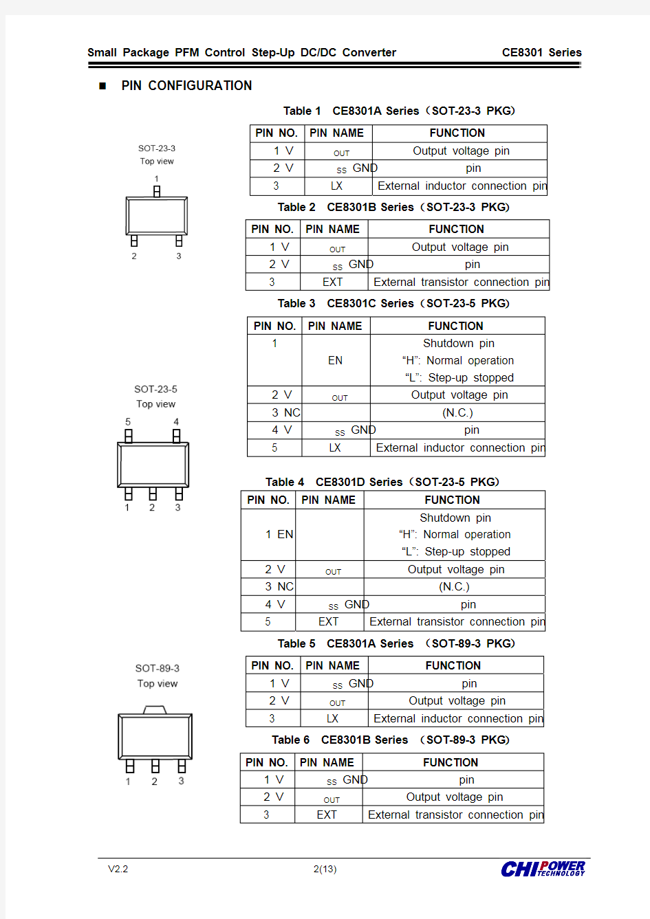
PIN CONFIGURATION
Table 1 CE8301A Series (SOT-23-3 PKG ) PIN NO.
PIN NAME
FUNCTION
1 V OUT Output voltage pin
2 V SS GND pin 3
LX
External inductor connection pin
Table 2 CE8301B Series (SOT-23-3 PKG ) PIN NO.
PIN NAME
FUNCTION 1 V OUT Output voltage pin
2 V SS GND pin 3
EXT
External transistor connection pin
Table 3 CE8301C Series (SOT-23-5 PKG ) PIN NO.
PIN NAME
FUNCTION 1
EN
Shutdown pin “H”: Normal operation “L”: Step-up stopped
2 V OUT Output voltage pin
3 NC (N.C.)
4 V SS GND pin
5
LX External inductor connection pin
Table 4 CE8301D Series (SOT-23-5 PKG ) PIN NO.
PIN NAME
FUNCTION 1 EN Shutdown pin
“H”: Normal operation “L”: Step-up stopped 2 V OUT Output voltage pin
3 NC (N.C.)
4 V SS GND pin
5
EXT
External transistor connection pin
Table 5 CE8301A Series (SOT-89-3 PKG )
PIN NO.
PIN NAME
FUNCTION 1 V SS GND pin 2 V OUT Output voltage pin
3
LX
External inductor connection pin
Table 6 CE8301B Series (SOT-89-3 PKG ) PIN NO.
PIN NAME
FUNCTION 1 V SS GND pin 2 V OUT Output voltage pin
3
EXT
External transistor connection pin
Table 7 CE8301C Series (SOT-89-5 PKG ) PIN NO.
PIN NAME
FUNCTION 1 NC (N.C.) 2 V OUT
Output voltage pin
3 EN Shutdown pin
“H”: Normal operation
“L”: Step-up stopped 4
LX
External inductor connection pin
5 V SS GND pin Table 8 CE8301D Series (SOT-89-5 PKG ) PIN NO.
PIN NAME
FUNCTION 1 NC (N.C.) 2 V OUT
Output voltage pin
3 EN Shutdown pin “H”: Normal operation
“L”: Step-up stopped 4
EXT
External transistor connection pin
5 V SS GND pin
Table 9 CE8301A Series (TO-92 PKG ) PIN NO.
PIN NAME
FUNCTION 1 V SS GND pin 2 V OUT Output voltage pin
3
LX External inductor connection pin
ABSOLUTE MAXIMUM RATINGS
(Unless otherwise specified, Ta=
25°C)
PARAMETER SYMBOL RATINGS UNITS V OUT pin voltage V OUT V SS -0.3 ~ V SS +8 V
EN pin voltage EN V SS -0.3 ~ V SS +8 V LX pin voltage V LX
V SS -0.3 ~ V SS +8 V
LX pin current
I LX 1000
mA
Power dissipation
SOT-23-3
PD
250 mW
SOT-23-5 250 mW
SOT-89-3 500 mW
TO-92 500 mW
Operating temperature T opr -40 ~+85 °C Storage temperature T stg -40 ~+125 °C Soldering Temperature & Time
T solder 260°C, 10s
ELECTRICAL CHARACTERISTICS
(Unless otherwise specified, Ta=25°C) PARAMETER SYNBOL CONDITIONS MIN TYP
MAX
UNITS
Output voltage V OUT-V OUT(S)
×0.98
V OUT
V OUT(S)
×1.02
V
Input voltage V IN--- 6 V Operation start voltage V ST1I OUT= 1 mA --0.9 V
Oscillation start voltage V ST2
No external parts, voltage
applied to V OUT LX pulled up
to V OUT via 300? resistor
--0.8 V
Current consumption 1I SS1V OUT=0.95
×V OUT
V OUT:3.0V-20 40 μA
V OUT:5.0V 30 60 μA
Current consumption 2I SS2V OUT=V OUT+0.5 V - 6 10 μA Current consumption
during shutdown
I SSS V EN = 0 V -- 1.0 μA
Switching current I SW V LX= 0.4 V 100 200 -mA
Switching transistor leakage current I SWQ
No external parts,
V LX=V OUT =8 V ,V EN = 0 V
-- 1.0 μA
Line regulation ?V OUT1V IN= 0.4×V OUT~
0.6×V OUT
-20 50 mV
Load regulation ?V OUT2I OUT= 10 μA ~ 50mA -20 50 mV
Maximum Oscillation
frequency f OSC
V OUT= 0.95×V OUT, measure
waveform at LX pin
100 KHz
Duty ratio 1 Duty1
V OUT= 0.95×V OUT,
measure waveform at
LX pin
70 78 85 %
Duty ratio 2 Duty2 Measure waveform at
LX pin with light load
-66 -%
Efficiency EFFI 85 %
Shutdown pin input
voltage V SH
V OUT=0.95×V OUT, judge
oscillation at LX pin
0.75 --V
V SL1
V OUT= 0.95×V OUT,
judge stop at LX pin
--0.3 V
Shutdown pin input
current I SH V EN=6V -0.1 -0.1 μA I SL V EN=0V -0.1 -0.1 μA
Remark:V IN =V OUT(S)×0.6 applied, I OUT=V OUT(S) / 250 ?
Shutdown function built-in type: EN pin is connected to V OUT
V ST1 only is suitable for CE8301A/C
V OUT(S) specified above is the set output voltage value, and V OUT is the typical value of
the actual output voltage.
■STANDARD CIRCUITS
Component: Inductor:47uH(Sumida) Diode:IN5817、IN5819 Capacitor:47uF/16V(Tantalum) Transistor:2SD1628G、2SD3279 NMOS:XP151、XP161 Base Resistor(Rb):1K ?
1、 CE8301A Circuits:
2、CE8301C Circuits:
3、CE8301B Circuits:
4、CE8301D Circuits:
TYPICAL PERFORMANCE CHARACTERISTICS
1. CE8301A30P:
a、V OUT vs. I OUT :
b、Efficiency vs. I OUT :
a、V OUT vs. I OUT :
b、Efficiency vs. I OUT :
3. CE8301A50P:
a、V OUT vs. I OUT :
b、Efficiency vs. I OUT :
4. CE8301B36P:
a、V OUT vs. I OUT :
b、Efficiency vs. I OUT :
a、V OUT vs. I OUT :
b、Efficiency vs. I OUT :
PACKAGE INFORMATION ● SOT-23-3
z TO-92
? Nanjing Chipower Electronics Inc.
Chipower cannot assume responsibility for use of any circuitry other than circuitry entirely embodied in a Chipower product. No circuit patent license, copyrights or other intellectual property rights are implied. Chipower reserves the right to make changes to their products or specifications without notice. Customers are advised to obtain the latest version of relevant information to verify, before placing orders, that information being relied on is current and complete.