ME60N04-V4.0 (080715)
Parameter
Symbol
Steady
Unit
Drain-Source Voltage V DSS 40 V Gate-Source Voltage V GSS ±20 V Continuous Drain Current (Tj=150℃,limited by package ) T C =25℃ I D 20 A T A =25℃
12
Pulsed Drain Current
I DM 50
A Avalanche Energy with Single Pulse(L=1mH) EAS 40 mJ Maximum Power Dissipation (Note A) T C =25℃ P D 30 W T A =25℃ 3 Operating Junction Temperature T J -55 to 150
℃ Thermal Resistance-Junction to Ambient(Note A) R θJA 42 ℃/W Thermal Resistance-Junction to Case(Note A) R θJC
4.3
℃/W
GENERAL DESCRIPTION
The ME60N04 is the N-Channel logic enhancement mode power field effect transistors are produced using high cell density DMOS trench technology. This high density process is especially tailored to minimize on-state resistance. These devices are particularly suited for low voltage application such as LCD inverter, computer power management and DC to DC converter circuits which need low in-line power loss.
FEATURES
● R DS(ON)≦12m ?@V GS =10V ● R DS(ON)≦17m ?@V GS =4.5V
● Super high density cell design for extremely low R DS(ON) ● Exceptional on-resistance and maximum DC current capability
APPLICATIONS
● Power Management ● DC/DC Converter
● LCD TV & Monitor Display inverter ● CCFL inverter
● Secondary Synchronous Rectification
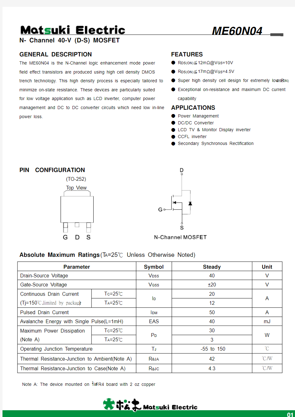
PIN CONFIGURATION
Absolute Maximum Ratings (T A =25℃ Unless Otherwise Noted)
Note A: The device mounted on 1in 2 FR4 board with 2 oz copper
(TO-252) Top View
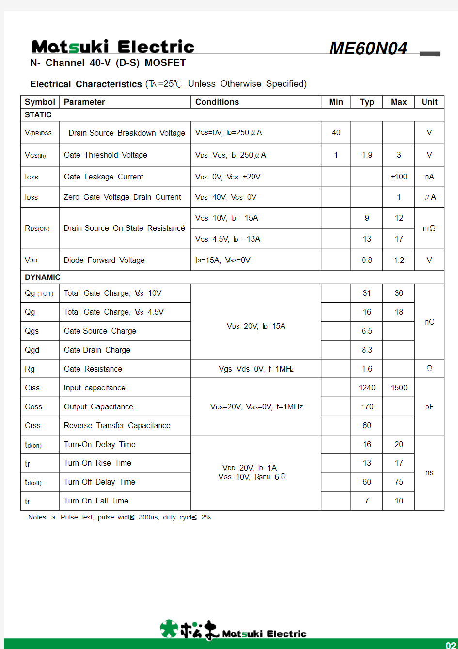
Symbol Parameter Conditions Min Typ Max Unit STATIC
V(BR)DSS Drain-Source Breakdown Voltage V GS=0V, I D=250μA 40 V V GS(th)Gate Threshold Voltage V DS=V GS, I D=250μA 1 1.9 3 V I GSS Gate Leakage Current V DS=0V, V GS=±20V ±100 nA I DSS Zero Gate Voltage Drain Current V DS=40V, V GS=0V 1 μA
R DS(ON)Drain-Source On-State Resistance a V GS=10V, I D= 15A 9 12
mΩV GS=4.5V, I D= 13A 13 17
V SD Diode Forward Voltage I S=15A, V GS=0V 0.8 1.2 V DYNAMIC
Qg (TOT)Total Gate Charge, V GS=10V
V DS=20V, I D=15A 31 36
nC
Qg Total Gate Charge, V GS=4.5V 16 18
Qgs Gate-Source Charge 6.5
Qgd Gate-Drain Charge 8.3
Rg Gate Resistance Vgs=Vds=0V, f=1MH Z 1.6 Ω
Ciss Input capacitance
V DS=20V, V GS=0V, f=1MHz 1240 1500
pF
Coss Output Capacitance 170 Crss Reverse Transfer Capacitance 60
t d(on)Turn-On Delay Time
V DD=20V, I D=1A
V GS=10V, R GEN=6Ω16 20
ns
t r Turn-On Rise Time 13 17 t d(off)Turn-Off Delay Time 60 75 t f Turn-On Fall Time 7 10 Electrical Characteristics (T A =25℃Unless Otherwise Specified)
Notes: a. Pulse test; pulse width ≦ 300us, duty cycle≦ 2%
Typical Characteristics (T J =25℃ Noted)
Typical Characteristics (T J =25℃ Noted)
SYMBOL
MILLIMETERS MIN MAX A 2.00 2.50 A1 1.1 1.3 B 0.30 0.70 B1 0.40 0.80 B2 0.60 1.00 C 0.40 0.60 D 5.30 5.70 D2 6.70 7.30 D3 2.20 3.00 H 9.20 9.80 E 6.30 6.70 E2 4.80 5.20 L 1.30 1.70 L1 0.90 1.50 L2 0.50 1.10 L3 0 0.30 P
2.40 2.80
TO-252 Package Outline