NE685M13-T3-A中文资料
NE685M13
NEC's NPN SILICON TRANSISTOR ?
NEW MINIATURE M13 PACKAGE:–Small transistor outline –1.0 X 0.5 X 0.5 mm
–Low profile / 0.50 mm package height –Flat lead style for better RF performance ?HIGH GAIN BANDWIDTH PRODUCT:f T = 12 GHz
?
LOW NOISE FIGURE:
NF = 1.5 dB at 2 GHz
FEATURES
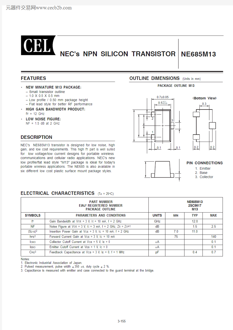
OUTLINE DIMENSIONS (Units in mm)
PACKAGE OUTLINE M13
PART NUMBER
NE685M13EIAJ 1 REGISTERED NUMBER
2SC5617PACKAGE OUTLINE
M13
SYMBOLS
PARAMETERS AND CONDITIONS
UNITS MIN
TYP MAX
f T Gain Bandwidth at V CE = 3 V, I C = 10 mA, f = 2 GHz GHz 12.0NF Noise Figure at V CE = 3 V, I C = 3 mA, f = 2 GHz, Z S = Z OPT dB 1.5 2.5|S 21E |2Insertion Power Gain at V CE = 3 V, I C = 10 mA, f = 2 GHz dB
7.011.0
h FE 2Forward Current Gain at V CE = 3 V, I C = 10 mA 75
140I CBO Collector Cutoff Current at V CB = 5 V, I E = 0μA 0.1I EBO Emitter Cutoff Current at V EB = 1 V, I C = 0
μA 0.1C RE 3
Feedback Capacitance at V CB = 3 V, I E = 0, f = 1 MHz
pF
0.4
0.7ELECTRICAL CHARACTERISTICS (T A = 25°C)
Notes:
1. Electronic Industrial Association of Japan.
2. Pulsed measurement, pulse width ≤ 350 μs, duty cycle ≤ 2 %.
3. Capacitance is measured with emitter and case connected to the guard terminal at the bridge.
DESCRIPTION
NEC's NE685M13 transistor is designed for low noise, high gain, and low cost requirements. This high f T part is well suited for low voltage/low current designs for portable wireless communications and cellular radio applications. NEC's new low profile/flat lead style "M13" package is ideal for today's portable wireless applications. The NE685 is also available in six different low cost plastic surface mount package styles.
1. Emitter
2. Base
3. Collector
PIN CONNECTIONS
(Bottom View)
Notes:
1.Operation in excess of any one of these parameters may result in permanent damage.
2. With device mounted on 1.08 cm 2 X 1.2 mm thick glass epoxy PCB.
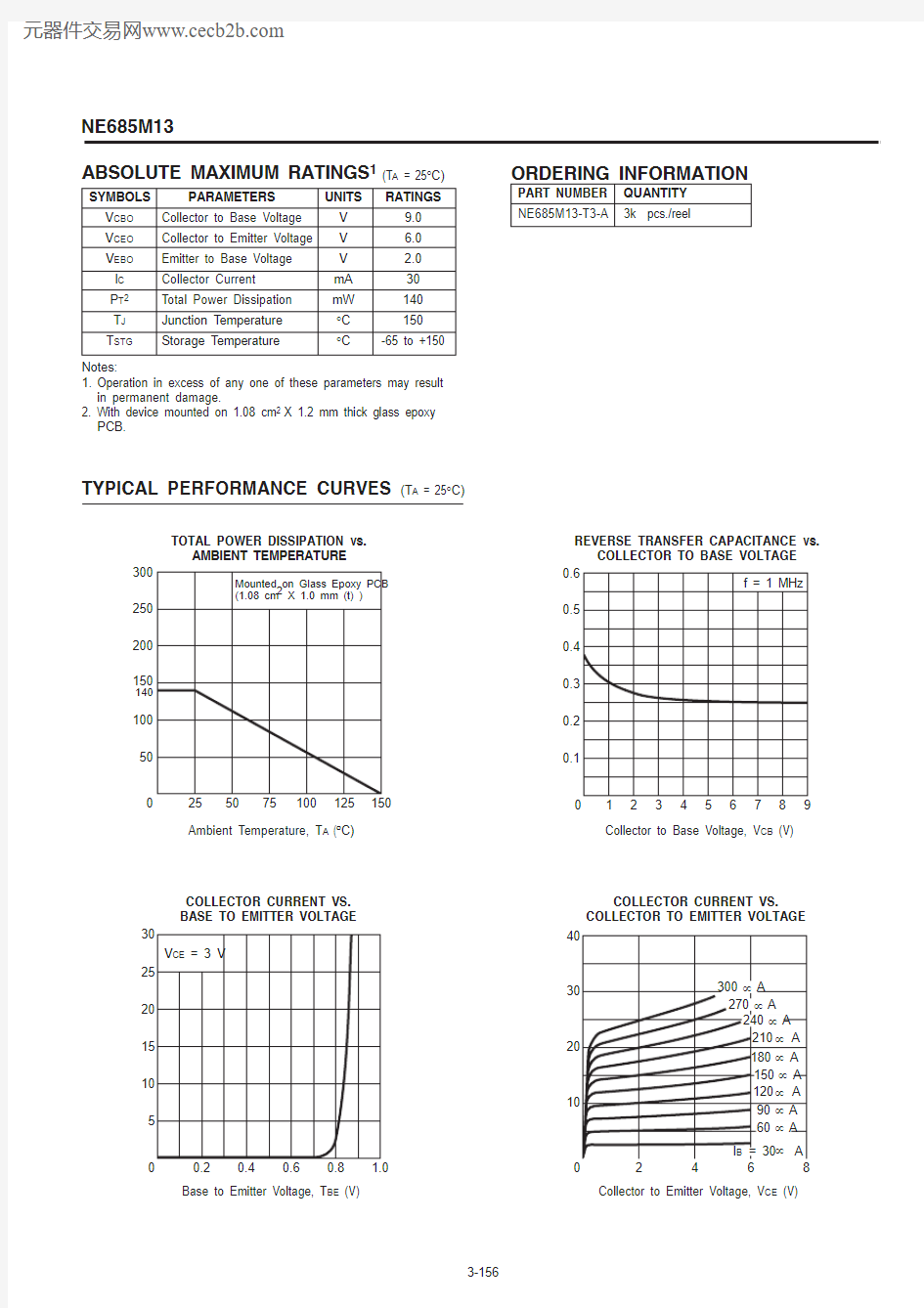
SYMBOLS PARAMETERS UNITS RATINGS
V CBO Collector to Base Voltage V 9.0V CEO Collector to Emitter Voltage V 6.0V EBO Emitter to Base Voltage V 2.0I C Collector Current mA 30P T 2Total Power Dissipation mW 140T J Junction Temperature °C 150T STG
Storage Temperature
°C
-65 to +150
ABSOLUTE MAXIMUM RATINGS 1 (T A = 25°C)
NE685M13
TYPICAL PERFORMANCE CURVES (T A = 25°C)
Collector to Base Voltage, V CB (V)
R e v e r s e T r a n s f e r C a p a c i t a n c e , C r e (p F )
REVERSE TRANSFER CAPACITANCE vs.
COLLECTOR TO BASE VOLTAGE Mounted on Glass Epoxy PCB
(1.08 cm 2
X 1.0 mm (t) )
300
250200150140
10050
0255075100125150
f = 1 MHz
0.6
0.50.40.30.20.1
0124567839
Ambient Temperature, T A (oC)T o t a l P o w e r D i s s i p a t i o n , P t o t (m W )
TOTAL POWER DISSIPATION vs.
AMBIENT TEMPERATURE
V CE = 3 V 30
2515105
2000.40.20.60.8 1.0Base to Emitter Voltage, T BE (V)C o l l e c t o r C u r r e n t ,
I C (m A )
COLLECTOR CURRENT VS.BASE TO EMITTER VOLTAGE
6
Collector to Emitter Voltage, V CE (V)
C o l l e c t o r C u r r e n t , I C (m A )
COLLECTOR CURRENT VS.
COLLECTOR TO EMITTER VOLTAGE
PART NUMBER QUANTITY NE685M13-T3-A
3k pcs./reel
ORDERING INFORMATION
NE685M13
GAIN BANDWIDTH PRODUCT vs.
COLLECTOR CURRENT
Frequency, f (GHz)I n s e r t i o n P o w e r G a i n |S 21e |2, (d B )
INSERTION POWER GAIN VS.
FREQUENCY
Frequency, f (GHz)
I n s e r t i o n P o w e r G a i n |S 21e |2, (d B )
INSERTION POWER GAIN VS.
FREQUENCY
Collector Current, I C (mA)
I n s e r t i o n P o w e r G a i n , I S 21e I 2
M a x i m u m A v a i l a b l e G a i n , M A G (d B )M a x i m u m S t a b l e G a i n , M S G (d B )
INSERTION POWER GAIN, MAG, MSG VS.
COLLECTOR CURRENT Collector Current, I C (mA)
I n s e r t i o n P o w e r G a i n , I S 21e I 2
M a x i m u m A v a i l a b l e G a i n , M A G (d B )M a x i m u m S t a b l e G a i n , M S G (d B )
INSERTION POWER GAIN, MAG, MSG VS.
COLLECTOR CURRENT
Collector Current, I C (mA)
G a i n B a n d w i d t h P r o d u c t , f T (G H z )
Collector Current, I C (mA)
D C C u r r e n t G a i n , h F E
DC CURRENT GAIN vs.COLLECTOR CURRENT
TYPICAL PERFORMANCE CURVES (T A = 25°C)
V CE = 3 V
1 000
100
101100.1
100
V CE = 3 V f = 2 GHz
161412108642
010
1
100
V CE = 1 V I C = 10 mA
35
3025201510500.1
1
10V CE = 3 V I C = 10 mA
35
3025201510500.1
1
10
Collector Current, I C (mA)
N o i s e F i g u r e N F , (d B )
NOISE FIGURE, ASSOCIATED GAIN VS.
COLLECTOR CURRENT
Collector Current, I C (mA)
N o i s e F i g u r e N F , (d B )
NOISE FIGURE, ASSOCIATED GAIN VS.
COLLECTOR CURRENT
INSERTION POWER GAIN, MAG, MSG VS.
COLLECTOR CURRENT
Collector Current, I C (mA)
I n s e r t i o n P o w e r G a i n , I S 21e I 2
M a x i m u m A v a i l a b l e G a i n , M A G (d B )M a x i m u m S t a b l e G a i n , M S G (d B )
Collector Current, I C (mA)
I n s e r t i o n P o w e r G a i n , I S 21e I 2
M a x i m u m A v a i l a b l e G a i n , M A G (d B )M a x i m u m S t a b l e G a i n , M S G (d B )
INSERTION POWER GAIN, MAG, MSG VS.
COLLECTOR CURRENT
TYPICAL PERFORMANCE CURVES (T A = 25°C)
NE685M13
A s s o c i a t e d G a i n , G a (d
B )
A s s o c i a t e d G a i n , G a (d
B )
TYPICAL PERFORMANCE CURVES (T A = 25°C)
NE685M13
Collector Current, I C (mA)
N o i s e F i g u r e N F , (d B )
NOISE FIGURE, ASSOCIATED GAIN VS.
COLLECTOR CURRENT
Collector Current, I C (mA)
N o i s e F i g u r e N F , (d B )
NOISE FIGURE, ASSOCIATED GAIN VS.
COLLECTOR CURRENT
A s s o c i a t e d G a i n , G a (d
B )
A s s o c i a t e d G a i n , G a (d
B )
NE685M13
TYPICAL SCATTERING PARAMETERS (T A = 25°C)
-j50
FREQUENCY
S 11
S 21
S 12
S 22
K
MAG 1GHz MAG ANG MAG ANG MAG ANG MAG ANG (dB)Note:
1.Gain Calculations:
NE685M13
V C = 2 V, I C = 5 mA
MAG = Maximum Available Gain
MSG = Maximum Stable Gain
0.1000.879-11.1810.895169.790.01785.460.980-8.260.0527.96 0.2000.854-24.7910.531159.270.03376.470.943-15.790.1325.05 0.3000.813-36.179.980150.160.04770.320.894-22.510.1923.25 0.4000.764-46.959.356142.000.05965.550.843-28.260.2421.980.5000.677-58.078.645133.160.06959.990.756-32.300.3721.00 0.6000.634-67.227.952127.180.07757.310.701-35.050.4320.16 0.7000.597-75.017.355122.040.08355.430.657-38.070.4719.460.8000.560-82.74 6.818117.170.08953.530.615-40.740.5118.82 0.9000.530-89.38 6.315113.030.09552.580.579-42.380.5618.241.0000.501-95.62 5.872109.140.09951.550.542-44.090.6117.731.1000.478-101.10 5.483105.720.10450.810.515-45.600.6517.22 1.2000.459-106.13 5.137102.650.10850.490.491-47.110.6816.79 1.4000.425-114.91 4.54397.140.11650.070.451-49.160.7615.941.6000.399-122.59 4.06892.390.12350.090.417-50.640.8215.181.8000.379-129.37 3.67888.200.13150.250.394-52.060.8814.492.0000.364-135.19 3.36984.360.13850.700.377-53.480.9213.872.2000.350-140.57 3.10380.910.14651.060.362-55.000.9613.27 2.4000.339-145.78 2.88277.590.15451.170.351-56.700.9912.73 2.6000.330-150.79 2.69574.450.16251.400.343-58.44 1.0211.43 2.8000.321-155.59 2.52971.460.17051.610.335-60.35 1.0410.49 3.0000.312-160.44 2.38668.560.17851.670.328-62.49 1.069.753.2000.306-165.34 2.26365.810.18651.550.324-65.12 1.089.16 3.4000.301-170.19 2.15063.120.19451.530.323-67.74 1.098.63 3.6000.296-175.11 2.04860.520.20251.430.323-70.53 1.108.143.8000.291-179.68 1.95758.060.21051.160.327-73.25 1.107.724.000
0.286
176.05
1.874
55.66
0.218
51.06
0.332
-75.87
1.117.33
MAG =
|S 21||S 12|
K - 1 ).2(K ±
? = S 11 S 22 - S 21 S 12
When K ≤ 1, MAG is undefined and MSG values are used.MSG =|S 21||S 12|, K = 1 + | ? | - |S 11| - |S 22|2222 |S 12 S 21
|
,+90o
+180o
NE685M13
TYPICAL SCATTERING PARAMETERS (T A = 25°C)
FREQUENCY
S 11
S 21
S 12
S 22
K
MAG 1GHz MAG ANG MAG ANG MAG ANG MAG ANG (dB)NE685M13
V C = 3 V, I C = 10 mA
0.1000.830-14.8915.406167.040.01579.150.969-9.820.1530.06 0.2000.791-30.2514.529155.170.02974.310.918-18.400.1826.960.3000.734-43.3513.385144.880.04168.950.852-25.660.2525.11 0.4000.675-55.2412.178136.080.05064.190.786-31.420.3223.86 0.5000.584-67.0210.911127.430.05859.860.690-34.940.4622.75 0.6000.541-76.489.839121.580.06457.870.631-37.080.5221.86 0.7000.506-84.408.943116.650.06956.900.586-39.460.5721.10 0.8000.473-92.178.163112.190.07555.960.546-41.460.6220.39 0.9000.448-98.627.477108.450.07955.530.513-42.470.6619.74 1.0000.423-104.84 6.891104.940.08355.340.478-43.520.7119.17 1.1000.405-110.11 6.385101.900.08855.240.455-44.520.7518.61 1.2000.390-114.95 5.94799.150.09255.230.435-45.570.7818.091.4000.364-123.47 5.21694.220.10055.770.401-46.750.8517.161.6000.344-130.71 4.64090.040.10956.130.373-47.510.9016.291.8000.329-137.11 4.17986.280.11756.730.355-48.390.9415.52 2.0000.318-142.56 3.80982.880.12657.150.341-49.390.9714.812.2000.308-147.52 3.49979.730.13557.350.330-50.56 1.0014.152.4000.300-152.37 3.24276.730.14457.600.322-51.97 1.0212.70 2.6000.294-157.24 3.02473.870.15357.620.316-53.62 1.0311.86 2.8000.287-161.72 2.83471.130.16257.530.310-55.48 1.0511.10 3.0000.282-166.38 2.67068.470.17157.390.304-57.60 1.0610.453.2000.277-170.99 2.52665.910.18057.270.302-60.04 1.079.89 3.4000.273-175.85 2.39763.400.18956.830.301-62.78 1.079.38 3.6000.270179.25 2.28260.990.19756.620.302-65.63 1.088.91 3.8000.266174.83 2.17958.670.20756.190.306-68.43 1.088.51 4.000
0.263
170.53
2.084
56.42
0.215
55.67
0.311
-71.13
1.088.11
j50
-j50
+90o
+180o
Note:
1.Gain Calculations:
MAG = Maximum Available Gain
MSG = Maximum Stable Gain
MAG =
|S 21||S 12|
K - 1 ).2(K ±
? = S 11 S 22 - S 21 S 12
When K ≤ 1, MAG is undefined and MSG values are used.MSG =|S 21||S 12|, K = 1 + | ? | - |S 11| - |S 22|2222 |S 12 S 21|
,
NE685M13 NONLINEAR MODEL
NE685M13
MODEL RANGE
Frequency:0.1 to 4.0 GHz Bias:V CE = 0.5 V to 3 V, I C = 0.5 mA to 20 mA Date:09/02
SCHEMATIC
Base
BJT NONLINEAR MODEL PARAMETERS (1)
(1) Gummel-Poon Model
Parameters
Q1 Parameters
Q1
IS 7e-16MJC 0.34BF 109XCJC 0.7 NF 1CJS 0VAF 15VJS 0.75IKF 0.19MJS 0ISE 7.9e-13FC 0.5 NE 2.19TF 2.5e-12BR 1 XTF 5.2NR 1.08 VTF 4.58VAR 12.4 ITF 0.011 IKR 0PTF 0ISC 0 TR 1e-9NC 2EG 1.11RE 1.3XTB 0RB 10 XTI 3RBM 8.34KF 0IRB 0.009 AF
1
RC 10CJE 0.4e-12VJE 0.812
MJE 0.5CJC 0.18e-12 VJC
0.75
Parameter Units time seconds (S)capacitance farads (F)inductance henries (H)resistance ohms (?)voltage volts (V)current
amps (A)
UNITS
Parameters 68533C CB 0.1e-12C CE 0.14e-12L B 0.35e-9L E 0.4e-9C CBPKG 0.05e-12C CEPKG 0.05e-12L BX 0.05e-9L CX 0.05e-9L EX
0.05e-9
ADDITIONAL PARAMETERS
Life Support Applications
These NEC products are not intended for use in life support devices, appliances, or systems where the malfunction of these products can reasonably be expected to result in personal injury. The customers of CEL using or selling these products for use in such applications do so at their own risk and agree to fully indemnify CEL for all damages resulting from such improper use or sale.
EXCLUSIVE NORTH AMERICAN AGENT FOR NEC RF, MICROWAVE & OPTOELECTRONIC SEMICONDUCTORS
? Headquarters ? 4590 Patrick Henry Drive ? Santa Clara, CA 95054-1817 ? (408) 988-3500 ? Telex 34-6393 ? FAX (408) 988-0279
Internet: https://www.360docs.net/doc/9217890082.html, 03/18/2002
4590 Patrick Henry Drive
Santa Clara, CA95054-1817
Telephone: (408)919-2500
Facsimile:(408) 988-0279
Subject:Compliance with EU Directives
CEL certifies, to its knowledge, that semiconductor and laser products detailed below are compliant with the requirements of European Union (EU) Directive 2002/95/EC Restriction on Use of Hazardous Substances in electrical and electronic equipment (RoHS) and the requirements of EU Directive 2003/11/EC Restriction on Penta and Octa BDE.
CEL Pb-free products have the same base part number with a suffix added. The suffix –A indicates that the device is Pb-free. The –AZ suffix is used to designate devices containing Pb which are exempted from the requirement of RoHS directive (*). In all cases the devices have Pb-free terminals. All devices with these suffixes meet the requirements of the RoHS directive.
This status is based on CEL’s understanding of the EU Directives and knowledge of the materials that go into its products as of the date of disclosure of this information.
Restricted Substance
per RoHS Concentration Limit per RoHS
(values are not yet fixed)
Concentration contained
in CEL devices
-A-AZ
Lead (Pb)< 1000 PPM
Not Detected(*) Mercury< 1000 PPM Not Detected
Cadmium< 100 PPM Not Detected Hexavalent Chromium< 1000 PPM Not Detected
PBB< 1000 PPM Not Detected
PBDE< 1000 PPM Not Detected
If you should have any additional questions regarding our devices and compliance to environmental standards, please do not hesitate to contact your local representative.
Important Information and Disclaimer: Information provided by CEL on its website or in other communications concerting the substance content of its products represents knowledge and belief as of the date that it is provided. CEL bases its knowledge and belief on information provided by third parties and makes no representation or warranty as to the accuracy of such information. Efforts are underway to better integrate information from third parties. CEL has taken and continues to take reasonable steps to provide representative and accurate information but may not have conducted destructive testing or chemical analysis on incoming materials and chemicals. CEL and CEL suppliers consider certain information to be proprietary,and thus CAS numbers and other limited information may not be available for release.
In no event shall CEL’s liability arising out of such information exceed the total purchase price of the CEL part(s) at issue sold by CEL to customer on an annual basis.
See CEL Terms and Conditions for additional clarification of warranties and liability.