HCF4098M013TR中文资料

1/10
September 2001s
RETRIGGERABLE/RESETTABLE CAPABILITY s TRIGGER AND RESET PROPAGATION DELAYS INDEPENDENT OF R X , C X s TRIGGERING FROM LEADING OR TRAILING EDGE s Q AND Q BUFFERED OUTPUT AVAILABLE s SEPARATE RESETS s WIDE RANGE OF OUTPUT PULSE WIDTHS s QUIESCENT CURRENT SPECIFIED UP TO 20V s 5V, 10V AND 15V PARAMETRIC RATINGS s INPUT LEAKAGE CURRENT
I I = 100nA (MAX) AT V DD = 18V T A = 25°C s 100% TESTED FOR QUIESCENT CURRENT s MEETS ALL REQUIREMENTS OF JEDEC JESD13B " STANDARD SPECIFICATIONS FOR DESCRIPTION OF B SERIES CMOS DEVICES"
DESCRIPTION
The HCF4098B is a monolithic integrated circuit fabricated in Metal Oxide Semiconductor technology available in DIP and SOP packages. The HCF4098B dual precision monostable multivibrator provides stable retriggerable/resettable one-shot operation for any fixed voltage timing application. An external resistor (R X ) and an external capacitor (C X ) control the timing for the circuit. Adjustment of R X and C X provides a wide range of output pulse widths from the Q and Q terminals. The time delay from trigger input to output transition (trigger propagation delay) and the time delay from reset input to output transition (reset propagation delay) and the time delay from reset input to output transition (reset propagation delay) are independent of R X and C X . Leading edge triggering (+TR) and trailing edge triggering (-TR) inputs are provided for triggering from either edge of an input pulse. An unused +TR input should be tied to V SS . An unused -TR input should be tied to V DD . A RESET (on low level) is provided for immediate termination of the output pulse or to prevent output pulses when power is turned on.
HCF4098B
DUAL MONOSTABLE MULTIVIBRATOR
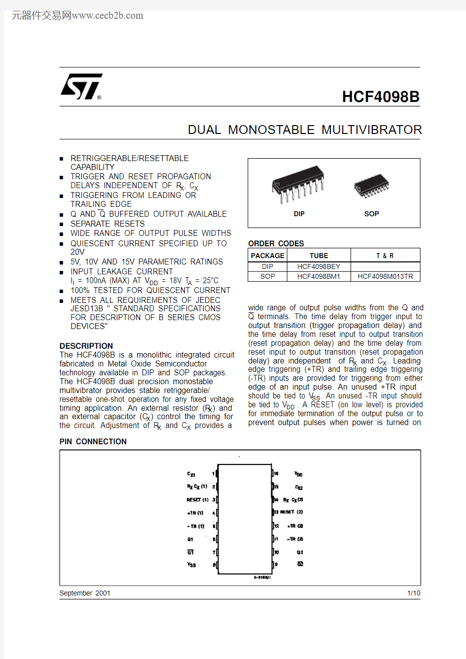
PIN CONNECTION
ORDER CODES
PACKAGE TUBE T & R DIP HCF4098BEY SOP
HCF4098BM1
HCF4098M013TR
HCF4098B
2/10
An unused RESET input should be tied to V DD .However, if an entire section of the HCF4098B is not used, its reset should be tied to V SS (see table 1). In normal operation the circuit triggers (extends the output pulse one period) on the application of each new trigger pulse. For operation in the non-retiggerable mode, Q is connected to -TR when leading edge triggering (+TR) is used or Q is connected to +TR when trailing edge triggering (-TR) is used. The time period (T) for this multivibrator can be calculated by : T = 1/2 R X C X for C X > 0.01μF. The min. value of external resistance, R X , is 5K ?. The max. values of external capacitance, C X , is 100 μF. The output pulse width has variations of ±2.5% typically, over the temperature range of -55 °C to 125 °C for C X =1000pF and R X = 100K ? . For power supply variation of ±5% typically , for V DD = 10V and 15V and ±1% typically for V DD = 5V at C X = 1000pF and R X = 5K ? .
IINPUT EQUIVALENT CIRCUIT
PIN DESCRIPTION
FUNCTIONAL DIAGRAM
PIN No SYMBOL NAME AND FUNCTION 4, 12+TR Leading Trigger Inputs 5, 11-TR Trailing Trigger Inputs 3, 13RESET Reset Inputs 1, 15C X 1, C X 2External Capacitors 2, 14R X C X 1R X C X 2External resistors to Vdd 6, 7Q1, Q1Ouputs Mono 110, 9Q2, Q2Outputs Mono 28V SS Negative Supply Voltage 16
V DD
Positive Supply Voltage
HCF4098B
3/10
TABLE 1 : Functional Terminal Connections
A Retriggerable one-shot multivibrator has an output pulse width which is extended on full time period (T) after application of the last trigger pulse.
A Non-Retriggerable one-shot multivibrator has a time period (T) referenced from the application of the firs trigger pulse.
LOGIC DIAGRAM
ABSOLUTE MAXIMUM RATINGS
Absolute Maximum Ratings are those values beyond which damage to the device may occur. Functional operation under these conditions is not implied.
All voltage values are referred to V SS pin voltage.
FUNCTION
V DD to Term. N °
V SS to Term. N °
Input Pulse to Term. N °
Other Connections
Mono (1)Mono (2)Mono (1)Mono (2)Mono (1)Mono (2)Mono (1)Mono (2)Leading Edge Trigger/
Retriggerable
3, 511, 13412Leading Edge Trigger/Non
Retriggerable 3134125, 7
11, 9
Trailing Edge Trigger/
Retriggerable
3134
12
511Trailing Edge Trigger/Non
Retriggerable 3135
11
4, 6
12, 10
Unused Section
5
11
3, 4
12, 13
Symbol Parameter
Value Unit V DD Supply Voltage -0.5 to +22V V I DC Input Voltage -0.5 to V DD + 0.5
V I I DC Input Current
± 10mA P D Power Dissipation per Package
200mW Power Dissipation per Output Transistor 100mW T op Operating Temperature -55 to +125°C T stg
Storage Temperature
-65 to +150
°C
HCF4098B
4/10
RECOMMENDED OPERATING CONDITIONS
DC SPECIFICATIONS
The Noise Margin for both "1" and "0" level is: 1V min. with V DD =5V, 2V min. with V DD =10V, 2.5V min. with V DD =15V
Symbol Parameter
Value Unit V DD Supply Voltage 3 to 20V V I Input Voltage
0 to V DD V T op
Operating Temperature
-55 to 125
°C
Symbol
Parameter
Test Condition
Value Unit
V I (V)V O (V)
|I O |(μA)V DD (V)
T A = 25°C -40 to 85°C -55 to 125°C Min.
Typ.Max.Min.
Max.Min.
Max.I L
Quiescent Current
0/550.0213030μA
0/10100.02260600/15150.024*******/20200.04
20
600
600
V OH
High Level Output Voltage
0/5<15 4.95 4.95 4.95V
0/10<1109.959.959.950/15<11514.95
14.95
14.95
V OL
Low Level Output Voltage
5/0<150.050.050.05V
10/0<1100.050.050.0515/0
<1150.050.05
0.05
V IH
High Level Input Voltage 0.5/4.5<15 3.5 3.5 3.5V
1/9<1107771.5/13.5<11511
11
11
V IL
Low Level Input Voltage 4.5/0.5<15 1.5 1.5 1.5V
9/1<11033313.5/1.5<1154
4
4
I OH
Output Drive Current
0/5 2.5<15-1.6-3.2-1.3-1.3mA
0/5 4.6<15-0.51-1-0.42-0.420/109.5<110-1.3-2.6-1.1-1.10/1513.5<115-3.4-6.8-2.8-2.8I OL
Output Sink Current
0/50.4<15-0.511-0.42-0.42mA 0/100.5<110-1.3 2.6-1.1-1.10/15 1.5<1
15-3.4
6.8-2.8
-2.8
I I Input Leakage Current
0/18
Any Input 18
±10-5±0.1±1
±1
μA C I
Input Capacitance
Any Input
5
7.5
pF
HCF4098B
5/10
DYNAMIC ELECTRICAL CHARACTERISTICS (T amb = 25°C, C L = 50pF, R L = 200K ?, t r = t f = 20 ns)
(*) Typical temperature coefficient for all V DD value is 0.3 %/°C.
Symbol
Parameter
Test Condition
Value (*)Unit
R X (K ?)C X (pF)V DD (V)Min.
Typ.Max.t PLH t PHL Propagation Delay Time
+TR or -TR to Q or Q 5 to 10000
>15
5250500ns 1012525015100200
t WH t WL
Trigger Pulse Width
5 to 10000
>15
514070ns
1060301540
20t TLH
Transition Time
5 to 10000
>155100200ns
1050100154080 t THL
Transition Time
5 to 10000
15 to 10000
5100200ns
10501001540805 to 10000
0.01μF to 0.1μF 5150300107515015651305 to 10000
0.1μF to 1μF
5250500101503001580160t PLH t PHL Propagation Delay Time
(Reset) 5 to 10000>155225450ns
101252501575150
t WR
Pulse Width (reset)
10015
5200100ns
1080401560301000
5120060010600300155002500.1μF
550250μs
1030151520
10t r, t f (TR)Rise or Fall Time (trigger)
5 to 15100μs Pulse Width Match Between Circuits in Same Package
10
10000
5510%
107.51515
7.5
15
HCF4098B
6/10
TEST CIRCUIT
L R L = 200K ?
R T = Z OUT of pulse generator (typically 50?)
HCF4098B
7/10
HCF4098B
Information furnished is believed to be accurate and reliable. However, STMicroelectronics assumes no responsibility for the consequences of use of such information nor for any infringement of patents or other rights of third parties which may result from its use. No license is granted by implication or otherwise under any patent or patent rights of STMicroelectronics. Specifications mentioned in this publication are subject to change without notice. This publication supersedes and replaces all information previously supplied. STMicroelectronics products are not authorized for use as critical components in life support devices or systems without express written approval of STMicroelectronics.
? The ST logo is a registered trademark of STMicroelectronics
? 2001 STMicroelectronics - Printed in Italy - All Rights Reserved
STMicroelectronics GROUP OF COMPANIES
Australia - Brazil - China - Finland - France - Germany - Hong Kong - India - Italy - Japan - Malaysia - Malta - Morocco
Singapore - Spain - Sweden - Switzerland - United Kingdom
? https://www.360docs.net/doc/9119078926.html,
10/10