LB1936
https://www.360docs.net/doc/a61513515.html,
Semiconductor Components Industries, LLC, 2013
LB1936V
Overview
The LB1936V is a 2-phase bipolar drive stepping motor driver IC that supports low-voltage drive. The LB1936V's miniature package and minimal number of external components reduces the required mounting area. It also provides high-efficiency motor drive and can reduce circuit current consumption. Since it provides a current detection pin and supports PWM control input, it can be used to implement current chopper control at the system level. The LB1936V is optimal for the stepping motor drive in scanners, digital cameras, and printers.
Features
? Low saturation voltage forward/reverse motor driver (V O sat = 0.25V at I O = 200mA) ? Two H-bridge channels
? Wide usable voltage range (Allowable voltage range : 2.5V to 9.5V, absolute maximum rating : 10.5V)
? Supports PWM input (Low power consumption can be achieved in slow delay mode that uses IN1/IN2 = H/H logic.) ? Motor (coil) current detection pin ? Built-in thermal shutdown circuit
? Miniature package (SSOP16 : 225mil)
Specifications
Absolute Maximum Ratings at Ta = 25°C
Parameter Symbol
Conditions
Ratings Unit
V CC max -0.3 to +10.5 V Maximum supply voltage
VS max
-0.3 to +10.5 V Maximum output voltage V OUT max VS+ VSF V Maximum input voltage V IN max
-0.3 to +8.0
V Ground pin source current IGND max Per channel 800 mA Allowable power dissipation Pd max When mounted on a circuit board * 740 mW Operating temperature Topr -20 to +85 °C Storage temperature
Tstg
-40 to +150
°C
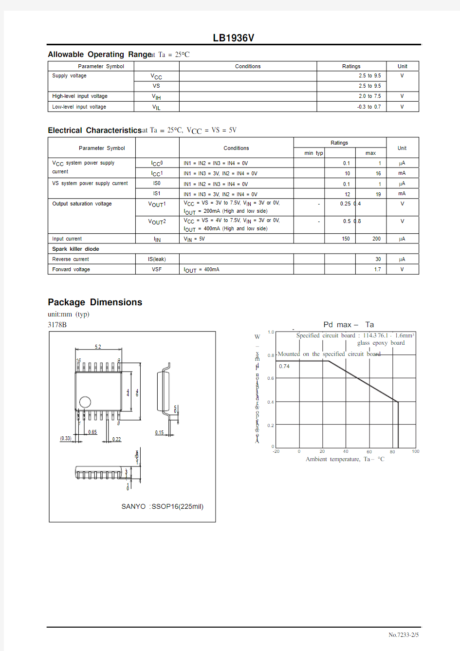
* Specified circuit board : 114.3 × 76.1 × 1.6mm 3, glass epoxy
Monolithic Digital IC 1-2 Phase Excitation Stepping Motor Driver
Allowable Operating Range at Ta = 25°C
Parameter Symbol
Conditions
Ratings Unit
V CC
2.5 to 9.5 Supply voltage
VS
2.5 to 9.5 V
High-level input voltage V IH 2.0 to 7.5 V Low-level input voltage
V IL
-0.3 to 0.7
V Electrical Characteristics at Ta = 25°C, V CC = VS = 5V
Ratings
Parameter Symbol
Conditions
min typ max
Unit
I CC 0 IN1 = IN2 = IN3 = IN4 = 0V 0.1 1 μA V CC system power supply
current
I CC 1 IN1 = IN3 = 3V, IN2 = IN4 = 0V 10 16 mA IS0 IN1 = IN2 = IN3 = IN4 = 0V 0.1 1 μA VS system power supply current
IS1
IN1 = IN3 = 3V, IN2 = IN4 = 0V
12
19
mA
V OUT 1 V CC = VS = 3V to 7.5V, V IN = 3V or 0V, I OUT = 200mA (High and low side)
-0.25 0.4 V Output saturation voltage
V OUT 2
V CC = VS = 4V to 7.5V, V IN = 3V or 0V,
I OUT = 400mA
(High and low side) -0.5 0.8 V Input current I IN
V
IN = 5V
150
200
μA
Spark killer diode Reverse current IS(leak)
30 μA Forward voltage
VSF
I OUT = 400mA
1.7
V
Package Dimensions
unit:mm (typ) 3178B
Ambient temperature, Ta –°C
A l l o w a b l e p o w e r d i s s i p a t i o n , P d m a x –W
Pin Assignment
Block Diagram
V CC
VS
IN1
IN2
S-GND
IN3
IN4
VS(NC)
RFG2
OUT4
OUT3
OUT2
OUT1
RFG1
P-GND
Top view
Truth Table
IN1 IN2 IN3 IN4 OUT1 OUT2 OUT3 OUT4 Output mode
L L off off (1) L H L H (2) H L H L (3) off H
(4)
H(*) H(*)
-
H off
-
(4)′
L L off off (5) L H
L H (6) H L H L
(7) off H
(8)
-
H(*) H(*)
-
H off
(8)′
L : low, H : high
*: The output logic mode when IN1/IN2 = H/H is determined by the immediately preceding IN1/IN2 mode.
The post-switching output modes will be as follows. When switching from (2): (4) When switching from (3): (4)'
When switching from (1): Undefined (Either (4) or (4)')
The modes when IN3/IN4 = H/H operate similarly as described below. When switching from (6): (8) When switching from (7): (8)'
When switching from (5): Undefined (Either (8) or (8)')
020
15
1055
150
0Supply voltage, V S –V
Input voltage, V IN –V
I -- V I -- V V (sat) -- I S u p p l y c u r r e n t , I C C –m A
Output current, I O –mA
O u t p u t s a t u r a t i o n v o l t a g e , V O (s a t ) –V
I n p u t c u r r e n t , I I N –μA
S u p p l y c u r r e n t , I S –m A
010
10
Ambient temperature, Ta –°C
Ambient temperature, Ta –°C
Ambient temperature, Ta –°C
I -- Ta
I -- Ta
V (sat) -- Ta
S u p p l y c u r r e n t , I C C –m A
O u t p u t s a t u r a t i o n v o l t a g e , V O (s a t ) –V
S u p p l y c u r r e n t , I s –m A