Study of wire bonding looping formation in the electronic packaging process using the three-dimen
Available online at https://www.360docs.net/doc/a63702509.html,
Finite Elements in Analysis and Design40(2004)263–286
https://www.360docs.net/doc/a63702509.html,/locate/?nel Study of wire bonding looping formation in the electronic packaging process using the three-dimensional
?nite element method
D.S.Liu?,Y.C.Chao,C.H.Wang
Department of Mechanical Engineering,National Chung Cheng University,160,
San-Hsing,Ming-Hsiung,Chia-Yi,621,Taiwan,ROC
Received18December2001;received in revised form17September2002;accepted8October2002 Abstract
This paper presents a three-dimensional?nite element model of the thermosonic wirebond looping process. The gold wire heat a ected zone load-displacement relationship was investigated using precision micro-force tensile tests.The temperature-dependent elastoplastic behaviors of gold wire were taken into account in the nonlinear?nite element model.Both the solid and equivalent shell wire models were used;exhibiting very close agreement,indicating that equivalent model was adequate.The simulation results were veri?ed against the experimental results.The standard triangle loop(STD2-Mode)and trapezoidal loop(LOW2-Mode)were simulated.The?nite element model closely predicted the pro?le of the tested loops.This model was used for an extensive looping factor parameter study.No obvious looping parameter e ects were observed for the STD2Mode.The loop shapes depend primarily on the wire properties,bonding pad distance and tier height. Both the looping and material parameters have signi?cant e ects on the loop shape for the LOW2Mode. Optimizing the reverse angles could reduce the stress on the wire.
?2002Elsevier B.V.All rights reserved.
Keywords:Wirebond;Gold wire;Heat a ected zone;Loop pro?le
1.Introduction
In recent years,as IC packaging development has moved towards higher power,smaller size, thinner dimensions,denser circuits and higher reliability,wire bonding is still the most commonly used bonding interconnection technique in?rst level microelectronic packages[1].In this intercon-nection method,bonding wires carry power and signals between the active semiconductor circuits ?Corresponding author.Tel.:+886-5-2720411;fax:+886-5-2720589.
E-mail address:imedsl@https://www.360docs.net/doc/a63702509.html,.tw(D.S.Liu).
0168-874X/$-see front matter?2002Elsevier B.V.All rights reserved.
doi:10.1016/S0168-874X(02)00226-3
264 D.S.Liu et al./Finite Elements in Analysis and Design40(2004)263–286
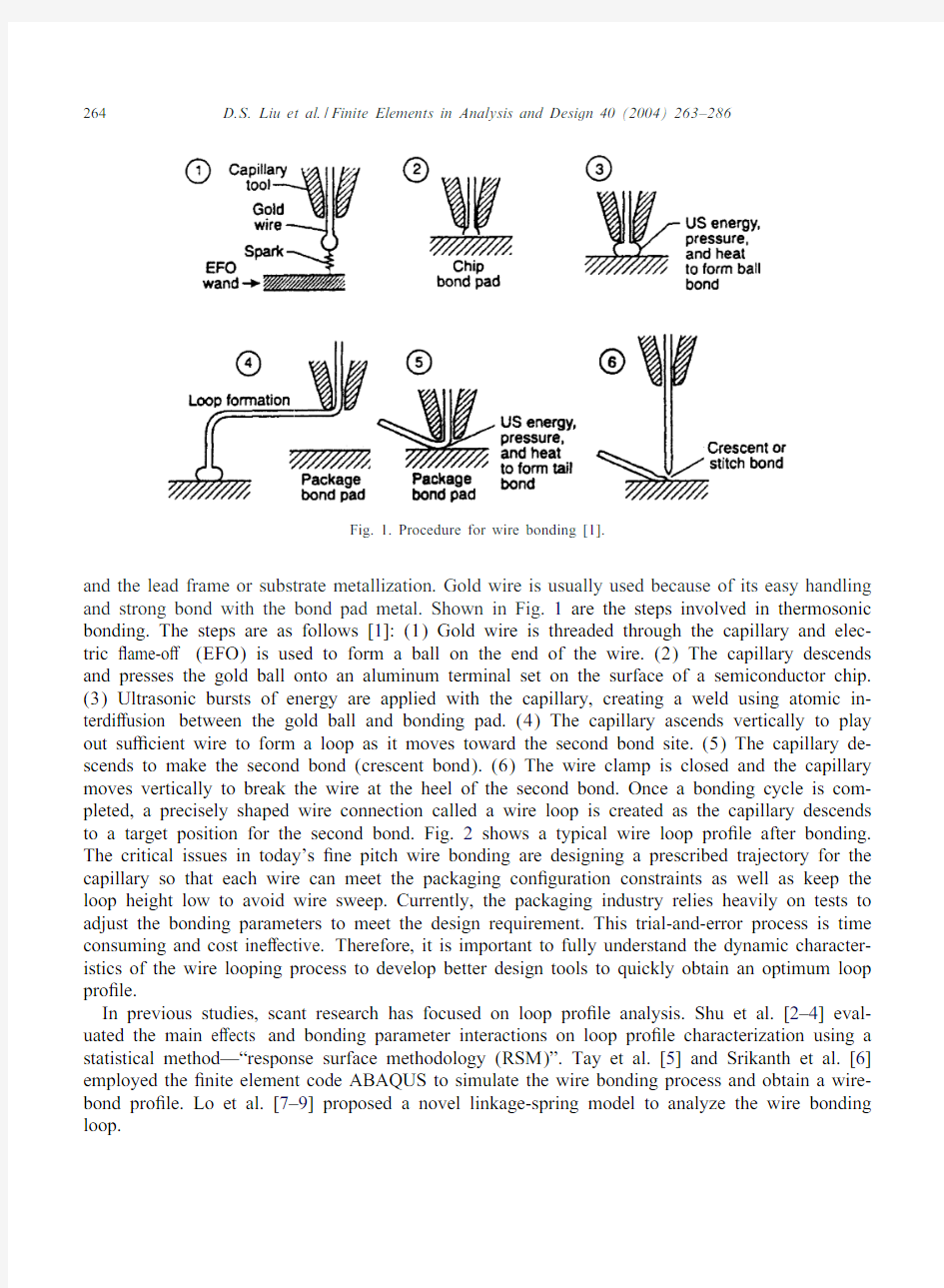
Fig.1.Procedure for wire bonding[1].
and the lead frame or substrate metallization.Gold wire is usually used because of its easy handling and strong bond with the bond pad metal.Shown in Fig.1are the steps involved in thermosonic bonding.The steps are as follows[1]:(1)Gold wire is threaded through the capillary and elec-tric ame-o (EFO)is used to form a ball on the end of the wire.(2)The capillary descends and presses the gold ball onto an aluminum terminal set on the surface of a semiconductor chip.
(3)Ultrasonic bursts of energy are applied with the capillary,creating a weld using atomic in-terdi usion between the gold ball and bonding pad.(4)The capillary ascends vertically to play out su cient wire to form a loop as it moves toward the second bond site.(5)The capillary de-scends to make the second bond(crescent bond).(6)The wire clamp is closed and the capillary moves vertically to break the wire at the heel of the second bond.Once a bonding cycle is com-pleted,a precisely shaped wire connection called a wire loop is created as the capillary descends to a target position for the second bond.Fig.2shows a typical wire loop pro?le after bonding. The critical issues in today’s?ne pitch wire bonding are designing a prescribed trajectory for the capillary so that each wire can meet the packaging con?guration constraints as well as keep the loop height low to avoid wire sweep.Currently,the packaging industry relies heavily on tests to adjust the bonding parameters to meet the design requirement.This trial-and-error process is time consuming and cost ine ective.Therefore,it is important to fully understand the dynamic character-istics of the wire looping process to develop better design tools to quickly obtain an optimum loop pro?le.
In previous studies,scant research has focused on loop pro?le analysis.Shu et al.[2–4]eval-uated the main e ects and bonding parameter interactions on loop pro?le characterization using a statistical method—“response surface methodology(RSM)”.Tay et al.[5]and Srikanth et al.[6] employed the?nite element code ABAQUS to simulate the wire bonding process and obtain a wire-bond pro?le.Lo et al.[7–9]proposed a novel linkage-spring model to analyze the wire bonding loop.
D.S.Liu et al./Finite Elements in Analysis and Design40(2004)263–286265
Fig.2.Typical thermosonic wirebond loop pro?le.
Besides the capillary trajectory,the wire material properties and EFO play important roles in determining the wire bonding pro?le.Ohno et al.[10]proposed a hardness distribution along the bonding wire corresponding to a V-shaped distribution.Qin et al.[11,12]and Huang et al.[13] performed numerical simulations and experimental works on wire ball formation.Qin et al.found that increasing the discharge current and decreasing the fuse time could decrease the heat a ected zone(HAZ)length.Tay et al.[5]simulated the transient temperature distribution along the wire using the?nite di erence method.
In all of the above studies,the wire properties used to perform the analysis,such as the elas-tic modulus and stress–strain curve,were given by the wire vendors at room temperature and high temperature(250?C).No studies involving the integration of more realistic stress–strain re-lations,especially in the HAZ adjacent to the ball-bond,were attempted due to lack of exper-imental data.Furthermore,little work has been reported on utilizing the three-dimensional?nite element method to simulate the wire looping process and study the bonding loop parameter e ect and residual stress distribution in the wire loop.Therefore,in this research,the looping parameter e ect was examined through computer simulations using a more realistic constitutive model of the gold wire.A newly designed tensile test method was developed to investigate the material proper-ties in the HAZ.The empirical constitutive model was proposed to predict the thermo-mechanical properties of gold wire.A dynamic?nite element code LS-DYNA version940[14]was used to perform the elasto-plastic large deformation contact analyses with the three-dimensional?nite el-ement https://www.360docs.net/doc/a63702509.html,paring the loop pro?les obtained from the computer simulation with the ac-tual wire bond specimens validated the accuracy of the simulation results.The agreement between the experimental and?nite element results was quite good.This computational model can be ap-plied to enhance the package reliability as well as speed up the proper wire bonder parameter settings.
266 D.S.Liu et al./Finite Elements in Analysis and Design40(2004)263–286
2.Material property of gold bonding wire
2.1.Constitutive relation of gold wire
The thermo-mechanical properties of gold wire are the most important factors in achieving a good computational model for simulating the looping process.A micro-force tensile test method for bonding wire was designed by the authors[15]according to ASTM F219-79testing standard[16]. An elastoplastic constitutive model was proposed to describe the behavior of gold bonding wire
[15].The wire used in this study is Tanaka Inc.25 m FA type gold wire.The FA gold wire is
a middle-strength type for middle loop height.There are four dopant elements in the1ppm range, such as Ag,Cu,Fe,Mg.The major dopant element is Ca in6ppm[17].The constitutive relation for FA25 m wire is written as follows:
=E0(1?e? )+E1 (1?T?);(1) E0(T)=228:9908?0:0778T?0:00015269T2;T unit:?C;(2) (T)=606:0641?0:7032T+0:001215T2;T unit:?C(3) E1=360;(4)
T?=
T?T room
T melt?T room
;T room=25?C and T melt=1070?C;(5)
where E0, ,E1is the material constants,T?,T room,and T melt are the homologous temperature,room temperature and melting temperature,respectively.The?rst term in Eq.(1)expresses the elastic and transition portion of the stress–strain curve.The second term in Eq.(1)denotes the stress–strain relationship in a fully plastic range.
A comparison of the predictions from Eq.(1)is presented in Fig.3.The results calculated from the constitutive model agree well with the experimental data.
2.2.Tensile test of HAZ
Heat energy from the ball formation process is conducted along the wire where the a ected region is recrystallized.The type of dopant added controls the recrystallization temperature of the material,which determines the length of this range called the HAZ.Up to now,the HAZ mechanical properties have never been tested.A new testing method was developed to investigate the tensile strength in the HAZ with various electronic torch input currents.Experiments were performed on an MTS-Tytron micro-force tester equipped with a100gf load cell at room temperature.The HAZ tensile test specimens were from actual wirebonding samples.The testing processes are listed below: (1)set the electronic torch current and1st,2nd bond point on the wirebonder,and then?nish the wirebonding loop.(2)Trim o the wire loop as close as possible to the second bond site.(3)Fix the HAZ specimen onto the microforce tester and start the tensile test.The HAZ specimen and test setup con?guration is illustrated in Fig.4.The material investigated in this study was20 m FA type gold wire.The HAZ specimens were bonded using a SHINKWA wire bonder at28,32,36mA
D.S.Liu et al./Finite Elements in Analysis and Design 40(2004)263–286
267
Strain(%)
S t r e s s (M P a )
https://www.360docs.net/doc/a63702509.html,parison of experimental data with model prediction for FA type gold
wire.
Gage Length (300 Fig.4.Con?guration of HAZ specimen and test setup.
electronic torch current.Tensile tests were performed at room temperature with a loading rate of 0.3mm/min.The gage length was 0.3mm.Fig.5compares the results for force versus displacement curve obtained over various electronic torch currents with the FA gold wire tensile test results at room temperature.No signi?cant di erent among the stress–strain curves is observed with various torch currents.The breaking load for the specimen with HAZ decreases about 25percent from 7.0to 5.2gf in comparison to the FA wire tensile test results at room temperature.The breaking position was located at 40–80 m from the neck portion.Furthermore,the decrease in breaking strain indicates
268 D.S.Liu et al./Finite Elements in Analysis and Design 40(2004)263–286
Displacement(mm)
F o r c e (g f )
Fig.5.Force vs displacement curve of 20 m FA gold wire and HAZ at room temperature.
that the mechanical properties of the material in the HAZ zone are more brittle than the original gold wire.
3.Wirebond looping simulation model 3.1.Finite element model
The con?guration of the typical wirebond model used in this study is shown in Fig.6.The model consists of a die,a pad,a lead frame,a ?rst ball bond,a capillary,a clamper and the gold wire.The wire diameter is 25 m.The capillary inner diameter is 38 m.The total wire length is 1400 m.The distance between ?rst bond and second bond is 1100 m.The chip height is 370 m.
In our study,a three-dimensional solid wire model was developed to simulate the wire bond loop formation https://www.360docs.net/doc/a63702509.html,paring the loop pro?les obtained from the computer simulation with the actual wire bond specimens validated the accuracy of the simulation results.A three-dimensional equivalent shell wire model was also developed in this study.The purpose of this model was to reduce the computation time so that the looping parameter e ects can be inves-tigated quickly through computer simulations.The shell element was a 4-node type,while the solid wire model was an 8-node brick element type.The model geometries,material properties,and boundary conditions used in the equivalent shell wire and solid wire models were the same except for the element type used in the wire model.The speci?c shell thickness was 6:29 m assigned to the shell wire maintain the weight of the shell wire equal to the real bonding wire.
D.S.Liu et al./Finite Elements in Analysis and Design40(2004)263–286269
Fig.6.The con?guration of wire bond model.
3.2.Material properties
The material properties of the gold wire are crucial in producing an accurate simulation.Two phenomena must be carefully examined.First,because of the large amount of heat energy transferred into the wire from the?rst bond formation process,the temperature distribution along the wire is not uniform.Second,the minimum mechanical strength and its position in the HAZ is important as a governing factor for the loop pro?le.Tay et al.[5]found that for a wire bond process with a duration of about0.15s,the temperature distribution will remain stable along the wire after?rst bond form (time?0:04s)was approximately a linear distribution that varied from200?C to room temperature. Therefore,in our study,the temperature distribution along the wire length was separated into four ranges.A constant temperature is given in each range,as shown in Fig.7,to approximate the linear decrease in each range.Once the temperature is de?ned in each range,the resultant temperature can be brought into the constitutive model proposed in Eqs.(1)–(5)to obtain the correlative stress–strain curve.Furthermore,according to the micro-force test results presented in the previous section,the minimum tensile strength at the HAZ should decrease by25%and be located40–80 m from the neck portion.Therefore,the HAZ was re-divided into?ve ranges and used the gold wire stress–strain curve at200?C as the reference strength.The minimum tensile strength assigned to range II declined by25%,and the strength in the other ranges was assumed to increase linearly back to the reference strength,as shown in Fig.8.A piecewise-linear-isotropic-plasticity material law in LS-DYNA3D was assigned to gold wire.The stress-strain curves in each part of the gold wire can be described by dividing the curve to several line segments and successively inputting the tangent modulus for each segment and e ective plastic strain value at each linking point.
270 D.S.Liu et al./Finite Elements in Analysis and Design 40(2004)263–286
6001400
Distance from neck of ball bond ( )
T e m p e r a t u r e d i s t r i b u t i o
n
10001200200m μFig.7.Temperature distribution along wire.
II
S t r e s s
(a)
(b)
200m
m
m m
m o C
Fig.8.(a,b)Wire property on heat a ected zone (HAZ).
All other parts of the FEM model,including the capillary,die,lead frame and wire clamper were much sti er than gold wire,so they are modeled as a rigid material with no temperature variation.Table 1summarizes the material properties used in this model.
D.S.Liu et al./Finite Elements in Analysis and Design40(2004)263–286271 Table1
Material properties used in the model
Part Density(g=cm3) E(GPa) y(MPa) u(MPa) Capillary 3.960.22370
Gold wire
200?C19.320.2864.5152214
190?C19.320.2864.7163216
180?C19.320.2864.8171218
160?C19.320.2865180220 HAZ I19.320.2860118182 HAZ II19.320.2850108169 HAZ III19.320.2854118182 HAZ IV19.320.2861128208 HAZ V19.320.2864140214
Fig.9.Equivalent shell wire tensile test model.
3.3.Material laws veri?cation and mesh density experiments
To verify the material law,a simple wire tensile test?nite element model with4-node shell elements was developed as shown in Fig.9.The wire length is400 m.The wire diameter is 25 m.The shell element size is10 m×5 m(length by width),and the thickness is6:29 m.The ?nite element model simulated the gold wire tensile test with one end?xed and the other moving at?xed strain rate.Fig.10shows the comparison between the simulation stress–strain relations with input material stress–strain curves.They agreed very well.This indicates that the material law developed in previous section is adequate.It also shows that reasonable simulation results should be obtained using an element size smaller than10 m×5 m.Therefore,an element dimension of 10 m×5 m(length by width)was selected for modeling the gold wire.The three-dimensional ?nite element model is shown in Fig.11.A total of16,131nodes and13,536solid elements were used to model the solid gold wire model.However,only2729nodes and2720shell elements were needed for the equivalent shell wire model.
272 D.S.Liu et al./Finite Elements in Analysis and Design 40(2004)263–286
Strain (%)
S t r e s s (M P a )
Fig.10.Simulation result of tensile test.
Fig.11.FEM mesh of wire bond model.
D.S.Liu et al./Finite Elements in Analysis and Design40(2004)263–286273
3.4.Loads and constraints
The?nite element model simulated the capillary movement along a speci?c trajectory.To keep the capillary moving on the x–z plane and vertical to the x–y plane,the nodes on the capillary,the rotation degree of freedom and the translation degree of freedom were restrained in the y direction. The nodes on the wire were free to translate and rotate in any direction,except for the?xed-end nodes on the ball bonds.The?xed boundary condition was given by restraining all of the degrees of freedom for the nodes on the lead frame,die,pad and ball bond.
The contact-interface was de?ned between the wire and the capillary to simulate the contact, however,the friction was negligible.In an actual bonding processes once the capillary ascends vertically to play out su cient wire to form the wire loop between the bonds,the wire clamps are closed at the highest point,causing the wire to move along the same trajectory as the capillary.To simulate this constraint condition,the contact interfaces were set at wire clamps and the end of the wire.Once the capillary ran to the top position of the movement path and started going downward to the second bond,the elements on the wire end between the wire clamps were free to move in the vertical direction between the clamps although their horizontal displacements were made the same as that of the capillary.
The HAZ and the turning range on the loop pro?le carry large plastic deformation;however,most of the other loop portions are deformed only in elastic range.According to the tensile testing results in Fig.3,the stress–stain relation of the gold wire did not very signi?cantly with temperature in the elastic range.Therefore the thermal contractions as the wire cools back to room temperature were not considered in this model.
4.Veri?cation of?nite element model
To verify the accuracy of the computational model,simulations were carried out with two types of bonding loop modes according to the actual wire bonding experiments:(a)STD2-Mode with a stan-dard triangle loop pro?le.(b)LOW2-Mode with a trapezoidal loop pro?le.The samples were bonded using a Shinkawa wire bonder.The pro?le for each sample was measured using a scanning electron microscope(SEM).Fig.12shows the capillary trajectory and loop pro?le of the STD2-Mode.The loop height indicates the distance between point G and point H.The capillary moves up to the middle of the HAZ for the inverse angle and an elliptical trace is chosen in the downward stage. The loop forming stages as shown in Fig.13.The capillary trajectory of the LOW2-Mode with dual reverse points can be applied to form a trapezoidal wire loop.As a result,the loop can be formed with the height of the wire loop kept low and contact prevented between the wire and the die.Fig.14shows the capillary trajectory and loop pro?le of the LOW2-Mode.The loop height indicates the distance between points H and I.The upper side length indicates the distance between points I and J.The wire loop forming stages are shown in Fig.15.
4.1.Solid and equilibrium shell wire model comparisons
Figs.16and17show the maximum Von-Mises stress from the LOW2-Mode simulations for the solid wire and equivalent shell wire models.As shown in the?gures,the agreement between the solid and shell simulations is very good except near the second bond point.This di erence
274 D.S.Liu et al./Finite Elements in Analysis and Design 40(2004)263–286
Reverse Length
Fig.12.Capillary trajectory and loop pro?le of STD2-Mode loop.
Fig.13.(a–e)Various stages of STD2-Mode loop formation.
D.S.Liu et al./Finite Elements in Analysis and Design 40(2004)263–286
275
2nd Reverse Length
Fig.14.Capillary trajectory and loop pro?le of LOW2-Mode loop.
Fig.15.(a–f)Various stages of LOW2-Mode loop formation.
276 D.S.Liu et al./Finite Elements in Analysis and Design40(2004)263–286
Fig.16.Simulation result of LOW2-Mode loop with shell wire model.
Fig.17.Simulation result of LOW2-Mode loop with solid wire model.
is due mainly to the solid elements not supporting the bending loads;therefore the wire near the capillary tip would form a large bend radius during the downward stage.This leads the pro?le near the second bond to contact the lead frame.The solid wire model and equivalent shell wire model stress distributions are very similar.This implies that the equivalent shell wire model is
D.S.Liu et al./Finite Elements in Analysis and Design 40(2004)263–286277
X-axial
(10E-03mm)
-400
-200
https://www.360docs.net/doc/a63702509.html,parison between simulated and actual wirebond pro?le for STD2-Mode loop.
X-axial (10E-03mm)
Z -a x i a l (10E -03
m m )
-400
-200
200
https://www.360docs.net/doc/a63702509.html,parison between simulated and actual wirebond pro?le for LOW2-Mode loop.
adequate for simulating the wire loop formation.This is a very good ?nding because the compu-tation time was decreased from 28h to 4h using the equivalent shell wire model.To reduce the computation time,the equivalent shell wire model was used to investigate the other parameters in this study.
4.2.Model veri?cation
The actual STD2and LOW2Mode pro?les were compared with the pro?les obtained from the three-dimensional wire computer simulations in Figs.18and 19.The loop obtained from the
278 D.S.Liu et al./Finite Elements in Analysis and Design40(2004)263–286 Table2
Comparison of simulated loop height with actual specimens
Loop mode Loop height( m)Discrepancy(%)
Experiment Simulation
STD2Mode110.39108.58 1.6
LOW2Mode100.93105.07 4.1
Fig.20.Von-Mises Stress distribution for STD2-Mode loop.
?nite element analysis closely simulated the experimental bonding loop.Table2compares the height of the actual wire bond pro?le with the height of the simulated wire bond pro?le.It can be seen that the discrepancy in the loop height was less than5%.The agreement between the simulation and experimental results demonstrate the reliability of the?nite element model predictions.
Figs.20and21show the Von-Mises stress distribution for each bonding mode.The maximum Von-Mises stress on both loops is about220MPa.The HAZ strain energy for the STD2-Mode is2:025N m and1:9526N m for the LOW2-Mode.Because of the strain energy discrepancy in the HAZ,the wire loop strength for the reverse trapezoidal loop would be stronger than that for a standard-triangle loop.This result agrees with the study by Hu[18]that indicated that neck-ing can be removed and pull strength increased when a reverse loop is introduced during the bonding process.The HAZ strain energy may be a good index to correlate the wire bond pull strength.
D.S.Liu et al./Finite Elements in Analysis and Design40(2004)263–286279
Fig.21.Von-Mises Stress distribution for LOW2-Mode loop.
5.Looping parameter study
In general,the wirebond loop pro?les are governed primarily by the material and looping param-eters.The material parameters primarily indicate the gold wire strength and the HAZ length,which depends on the EFO.The looping parameters include the capillary movement trajectory(looping mode),wire length,reverse angle,reverse length and bonding speed.Adapted looping parame-ters can reduce the loop height and increase the reliability.The looping parameters on both the LOW2-Mode and STD2-Mode considered here included the reverse angle,reverse length and wire length.
5.1.STD2-mode(standard triangle mode)
Fig.22shows the capillary trajectory of the STD2-Mode with various reverse angles.As the reverse angle increases,the highest capillary moving position descends to?x the wire length.The reverse length is180 m in these cases.Loop pro?les with various reverse angles are shown in Fig.23,from which it may be seen that the loop height increases slightly and bevel edge drops with the increment of reverse angle.Fig.24shows that the reverse length has no obvious e ect on the looping pro?le.From the above,the reverse angle and reverse length have no obvious e ects on the looping pro?le for the STD2-Mode.In other words,the STD-2Mode loop pro?le is dominated mainly by the material parameters and bond pad con?gurations instead of the looping parameters.
5.2.LOW2-mode(reverse trapezoidal mode)
The2nd reverse angle e ects were studied?rst.Fig.25shows the capillary path with a?xed 15?1st reverse angle and di erent2nd reverse angle.The?rst reverse length is110 m,and the
280 D.S.Liu et al./Finite Elements in Analysis and Design 40(2004)263–286
X-axial (10E-03
mm)
Fig.22.Capillary trajectory for STD2-Mode loop with di erent reverse
angle.
Z -a x i a l (10E -03m m )
-400
-200
https://www.360docs.net/doc/a63702509.html,parison of STD2-Mode loop with di erent reverse angle.
second reverse length is 520 m in these cases.Two phenomena were observed for di erent loops by increasing the 2nd reverse angle,as shown in Fig.26.First,the loop shape tends to be more trapezoidal with the 2nd reverse angle.This implies that the purpose of the 2nd reverse angle is to form a trapezoidal pro?le.Second,the loop height varies from 140to 110 m with a change in the increment of the 2nd reverse angle from 15?to 50?.The HAZ Von-Mises stress distribution for loops with various 2nd reverse angles is shown in Fig.27.The maximum Von-mises stress
D.S.Liu et al./Finite Elements in Analysis and Design 40(2004)263–286281
X-axial(10E-03mm)
-400
-200
https://www.360docs.net/doc/a63702509.html,parison of STD2-Mode loop with di erent reverse length.
X-axial (10E-03mm)
Fig.25.Capillary trajectory for LOW2-Mode loop with di erent 2nd reverse angle.
on the HAZ decreases with a change in the increment of the 2nd reverse angle from 15?to 30?.The maximum Von-Mises stress on the HAZ increases as the 2nd reverse angle becomes greater than 30?.Furthermore,obvious necking is observed when the 2nd reverse angle is greater than 40?.From the above,the increment of the 2nd reverse angle not only decreases the loop height,but also decreases the loop strength.The adapted 2nd reverse angle is from 15?to 30?.
282 D.S.Liu et al./Finite Elements in Analysis and Design 40(2004)263–286
X-axial(10E-03mm)
Z -a x i a l (10E -03m m )
-400
-200
https://www.360docs.net/doc/a63702509.html,parison
of LOW2-Mode loop with di erent 2nd reverse angle (1st reverse angle =15?).
Fig.27.Von-Mises stress distribution on HAZ for LOW2-Mode loop with various 2nd reverse angle (a)?=15?,(b)?=30?,(c)?=40?and (d)?=50?(1st reverse angle =15?).
The e ects on the 1st reverse angle were investigated next.Fig.28shows comparisons between the loop pro?les with a ?xed 2nd reverse angle and various 1st reverse angles.The ?rst reverse length is 110 m,and the second reverse length is 520 m in these cases.As the 1st reverse angle
半导体材料的发展现状与趋势
半导体材料与器件发展趋势总结 材料是人类社会发展的物质基础与先导。每一种重大新材料的发现和应用都把人类支配自然的能力提高到一个全新的高度。材料已成为人类发晨的里程碑。本世纪中期单晶硅材料和半导体晶体管的发明及其硅集成电路的研究成功,导致了电子工业大革命。使微电子技术和计算机技术得到飞速发展。从20世纪70年代的初期,石英光纤材料和光学纤维的研制成功,以及GaAs等Ⅲ-Ⅴ族化合物的材料的研制成功与半导体激光器的发明,使光纤通信成为可能,目前光纤已四通八达。我们知道,每一束光纤,可以传输成千上万甚至上百万路电话,这与激光器的发明以及石英光纤材料、光纤技术的发展是密不可分的。超晶格概念的提出MBE、MOCVD先进生长技术发展和完善以及超品格量子阱材料包括一维量子线、零维量子点材料的研制成功。彻底改变了光电器件的设计思想。使半导体器件的设计与制造从过去的杂质工程发展到能带工程。出现了以“电学特性和光学特性的剪裁”为特征的新范畴,使人类跨入到以量子效应为基础和低维结构为特征的固态量子器件和电路的新时代,并极有可能触发新的技术革命。半导体微电子和光电子材料已成为21世纪信息社会的二大支柱高技术产业的基础材料。它的发展对高速计算、大容量信息通信、存储、处理、电子对抗、武器装备的微型化与智能化和国民经济的发展以及国家的安全等都具有非常重要的意义。 一、几种重要的半导体材料的发展现状与趋势 1.硅单晶材料 硅单晶材料是现代半导体器件、集成电路和微电子工业的基础。目前微电子的器件和电路,其中有90%到95%都是用硅材料来制作的。那么随着硅单晶材料的进一步发展,还存在着一些问题亟待解决。硅单晶材料是从石英的坩埚里面拉出来的,它用石墨作为加热器。所以,来自石英里的二氧化硅中氧以及加热器的碳的污染,使硅材料里面包含着大量的过饱和氧和碳杂质。过饱和氧的污染,随着硅单晶直径的增大,长度的加长,它的分布也变得不均匀;这就是说材料的均匀性就会遇到问题。杂质和缺陷分布的不均匀,会使硅材料在进一步提高电路集成度应用的时候遇到困难。特别是过饱和的氧,在器件和电路的制作过程中,它要发生沉淀,沉淀时的体积要增大,会导致缺陷产生,这将直接影响器件和电路的性能。因此,为了克服这个困难,满足超大规模集成电路的集成度的进一步提高,人们不得不采用硅外延片,就是说在硅的衬底上外延生长的硅薄膜。这样,可以有效地避免氧和碳等杂质的污染,同时也会提高材料的纯度以及掺杂的均匀性。利用外延方法,还可以获得界面非常陡、过渡区非常窄的结,这样对功率器件的研制和集成电路集成度进一步提高都是非常有好处的。这种材料现在的研究现状是6英寸的硅外延片已用于工业的生产,8英寸的硅外延片,也正在从实验室走向工业生产;更大直径的外延设备也正在研制过程中。 除此之外,还有一些大功率器件,一些抗辐照的器件和电路等,也需要高纯区熔硅单晶。区熔硅单晶与直拉硅单晶拉制条件是不一样的,它在生长时,不与石英容器接触,材料的纯度可以很高;利用这种材料,采用中子掺杂的办法,制成N或P型材料,用于大功率器件及电路的研制,特别是在空间用的抗辐照器件和电路方面,它有着很好的应用前景。当然还有以硅材料为基础的SOI材料,也就是半导体/氧化物/绝缘体之意,这种材料在空间得到了广泛的应用。总之,从提高集成电路的成品率,降低成本来看的话,增大硅单晶的直径,仍然是一个大趋势;因为,只有材料的直径增大,电路的成本才会下降。我们知道硅技术有个摩尔定律,每隔18个月它的集成度就翻一番,它的价格就掉一半,价格下降是同硅的直径的增大密切相关的。在一个大圆片上跟一个小圆片上,工艺加工条件相同,但出的芯片数量则不同;所以说,增大硅的直径,仍然是硅单晶材料发展的一个大趋势。那我们从提高硅的
半导体材料的发展现状与趋势
半导体材料的发展现状与趋势
半导体材料与器件发展趋势总结 材料是人类社会发展的物质基础与先导。每一种重大新材料的发现和应用都把人类支配自然的能力提高到一个全新的高度。材料已成为人类发晨的里程碑。本世纪中期单晶硅材料和半导体晶体管的发明及其硅集成电路的研究成功,导致了电子工业大革命。使微电子技术和计算机技术得到飞速发展。从20世纪70年代的初期,石英光纤材料和光学纤维的研制成功,以及GaAs 等Ⅲ-Ⅴ族化合物的材料的研制成功与半导体激光器的发明,使光纤通信成为可能,目前光纤已四通八达。我们知道,每一束光纤,可以传输成千上万甚至上百万路电话,这与激光器的发明以及石英光纤材料、光纤技术的发展是密不可分的。超晶格概念的提出MBE、MOCVD先进生长技术发展和完善以及超品格量子阱材料包括一维量子线、零维量子点材料的研制成功。彻底改变了光电器件的设计思想。使半导体器件的设计与制造从过去的杂质工程发展到能带工程。出现了以“电学特性和光学特性的剪裁”为特征的新范畴,使人类跨入到以量子效应为基础和低维结构
的制作过程中,它要发生沉淀,沉淀时的体积要增大,会导致缺陷产生,这将直接影响器件和电路的性能。因此,为了克服这个困难,满足超大规模集成电路的集成度的进一步提高,人们不得不采用硅外延片,就是说在硅的衬底上外延生长的硅薄膜。这样,可以有效地避免氧和碳等杂质的污染,同时也会提高材料的纯度以及掺杂的均匀性。利用外延方法,还可以获得界面非常陡、过渡区非常窄的结,这样对功率器件的研制和集成电路集成度进一步提高都是非常有好处的。这种材料现在的研究现状是6英寸的硅外延片已用于工业的生产,8英寸的硅外延片,也正在从实验室走向工业生产;更大直径的外延设备也正在研制过程中。 除此之外,还有一些大功率器件,一些抗辐照的器件和电路等,也需要高纯区熔硅单晶。区熔硅单晶与直拉硅单晶拉制条件是不一样的,它在生长时,不与石英容器接触,材料的纯度可以很高;利用这种材料,采用中子掺杂的办法,制成N或P型材料,用于大功率器件及电路的研制,特别是在空间用的抗辐照器件和电路方面,
(新)半导体材料发展现状及趋势 李霄 1111044081
序号:3 半导体材料的发展现状及趋势 姓名:李霄 学号:1111044081 班级:电科1103 科目:微电子设计导论 二〇一三年12 月23 日
半导体材料的发展进展近况及趋向 引言:随着全球科技的飞速发展成长,半导体材料在科技进展中的首要性毋庸置疑,半导体的发展进展历史很短,但半导体材料彻底改变了我们的生活,从半导体材料的发展历程、半导体材料的特性、半导体材料的种类、半导体材料的制备、半导体材料的发展。从中我们可以感悟到半导体材料的重要性 关键词:半导体、半导体材料。 一、半导体材料的进展历程 20世纪50年代,锗在半导体产业中占主导位置,但锗半导体器件的耐高温和辐射性能机能较差,到20世纪60年代后期逐步被硅材料代替。用硅制作的半导体器件,耐高温和抗辐射机能较好,非常适合制作大功率器件。因而,硅已经成为运用最多的一种半导体材料,现在的集成电路多半是用硅材料制作的。二是化合物半导体,它是由两种或者两种以上的元素化合而成的半导体材料。它的种类不少,主要的有砷化镓(GaAs)、磷化铟(InP)、锑化铟(InSb)、氮化镓(GaN)、碳化硅(SiC)、硫化镉(CdS)等。此中砷化镓是除了硅以外研讨最深切、运用最普遍的半导体材料。氮化镓可以与氮化铟(Eg=1.9eV)、氮化铝(Eg=6.2eV)构成合金InGaN、AlGaN,如许可以调制禁带宽度,进而调理发光管、激光管等的波长。三是非晶半导体。上面介绍的都是拥有晶格构造的半导体材料,在这些材料中原子布列拥有对称性和周期性。但是,一些不拥有长程有序的无定形固体也拥有显著的半导体特征。非晶半导体的种类繁多,大体上也可按晶态物质的归类方式来分类。从现在}研讨的深度来看,很有适用价值的非晶半导体材料首推氢化非晶硅(α-SiH)及其合金材料(α-SiC:H、α-SiN:H),可以用于低本钱太阳能电池和静电光敏感材料。非晶Se(α-Se)、硫系玻璃及氧化物玻璃等非晶半导体在传感器、开关电路及信息存储方面也有普遍的运用远景。四是有机半导体,比方芳香族有机化合物就拥有典范的半导体特征。有机半导体的电导特征研讨可能对于生物体内的基础物理历程研究起着重大推进作用,是半导体研讨的一个热点领域,此中有机发光二极管(OLED)的研讨尤为受到人们的看重。 二、半导体材料的特性 半导体材料是常温下导电性介于导电材料以及绝缘材料之间的一类功效材
研究生《高等半导体器件物理》试题
2014级研究生《高等半导体器件物理》试题 1.简单说明抛物线性能能带和非抛物线性能带的能带结构以及各自 的特点、应用。 2.试描述载流子的速度过冲过程和弹道输运过程,以及它们在实际 半导体器件中的应用。 3.什么是半导体超晶格?半导体器件中主要的量子结构有哪些? 半导体超晶格:两种或者两种以上不同组分或者不同导电类型超薄层材料,交替堆叠形成多个周期结构,如果每层的厚度足够薄,以致其厚度小于电子在该材料中的德布罗意波的波长, 这种周期变化的超薄多层结构就叫做超晶格. 主要的量子结构:超晶格中, 周期交替变化的超薄层的厚度很薄,相临势阱中的电子波函数能够互相交叠, 势阱中的电子能态虽然是分立的, 但已被展宽. 如果限制势阱的势垒进度足够厚, 大于德布罗意波的波长, 那么不同势阱中的波函数不再交叠, 势阱中电子的能量状态变为分立的能级. 这种结构称之为量子阱( QW).在上述结构中,电子只在x 方向上有势垒的限制, 即一维限制,而在y , z 两个方向上是二维自由的. 如果进一步增加限制的维度,则构成量子线和量子点. 对于量子线而言, 电子在x , y 两个方向上都受到势垒限制; 对于量子点来说, 在x , y , z 三个方向上都有势垒限制. 我们通常将这些量子结构称为低维结构, 即量子阱、量子线和量子点分别为二维、一维和零维量子结构. 4.PHEMT的基本结构、工作原理以及电学特点。 5.隧道谐振二极管的主要工作特点,RITD的改进优势有哪些? 6.突变发射结、缓变基区HBT的工作原理、特点及其应用。 7.举例讨论半导体异质结光电器件的性能。
参考文献: 1.沃纳,半导体器件电子学,电子工业出版社,2005 2.施敏,现代半导体器件物理,科学出版社,2002 3.王良臣等,半导体量子器件物理讲座(第一讲~第七讲),物理(期刊),2001~2002
院士讲材料——半导体材料的发展现状与趋势汇总
主持人: 观众朋友,欢迎您来到CETV学术报告厅,最近美国的一家公司生产出一千兆的芯片,它是超微技术发展史上的一个分水岭,个人电脑业的发展,也将步入一个新的历史阶段,对整个信息业来说,它的意义不亚于飞行速度突破音速的极限,当然整个技术上的突破,也要依赖于以硅材料为基础的大规模集成电路的进一步微型化,50年代以来,随着半导体材料的发现与晶体管的发明,以硅为主的半导体材料,成为整个信息社会的支柱,成为微电子、光电子等高技术产业的核心与基础,这个情况,将会持续到下个世纪的中叶,当然,面对更大信息量的需求,硅电子技术也有它的极限,将会出现新的、替补性的半导体材料。关于半导体材料的发展现状与发展趋势,请您收看中国科学院王占国院士的学术报告。 王占国: 材料已经成为人类历史发展的里程碑,从本世纪的中期开始,硅材料的发现和硅晶体管的发明以及五十年代初期的以硅为基的集成电路的发展,导致了电子工业大革命。今天,因特网、计算机的到户,这与微电子技术的发展是密不可分的,也就是说以硅为基础的微电子技术的发展,彻底地改变了世界的政治、经济的格局,也改变着整个世界军事对抗的形式,同时也深刻影响着人们的生活方式。今天如果没有了计算机,没有了网络,没有了通信,世界会是什么样子,那是可想而知的。从20世纪70年代的初期,石英光纤材料和光学纤维的研制成功,以及GaAs 等Ⅲ-Ⅴ族化合物的材料的研制成功与半导体激光器的发明,使光纤通信成为可能,目前光纤已四通八达。我们知道,每一束光纤,可以传输成千上万甚至上百万路电话,这与激光器的发明以及石英光纤材料、光纤技术的发展是密不可分的。 70年代超晶格概念的提出,新的生长设备,像分子束外延和金属有机化合物化学汽相淀积等技术的发展,以及超晶格、量子阱材料的研制成功,使半导体材料和器件的设计思想发生了彻底的改变。就硅基材料的器件和电路而言,它是靠P型与N型掺杂和PN结技术来制备二极管、晶体管和集成电路的。然而基于超晶格、量子阱材料的器件和电路的性质,则不依赖于杂质行为,而是由能带工程设计决定的。也就是说,材料和器件的光学与电学性质,可以通过能带的设计来实现。设计思想从杂质工程发展到能带工程,以及建立在超晶格、量子阱等半导体微结构材料基础上的新型量子器件,极有可能引发新的技术革命。从微电子技术短短50年的发展历史来看,半导体材料的发展对高速计算、大容量信息通信、存储、处理、电子对抗、武器装备的微型化与智能化和国民经济的发展以及国家的安全等都具有非常重要的意义。 现在,我来讲一讲几种重要的半导体材料的发展现状与趋势。我们首先来介绍硅单晶材料。硅单晶材料是现代半导体器件、集成电路和微电子工业的基础。目前微电子的器件和电路,其中有90%到95%都是用硅材料来制作的。根据预测,到2000年底,它的规模将达到60多亿平方英寸,整个硅单晶材料的产量将达到1万吨以上。目前,8英寸的硅片,已大规模地应用于集成电路的生产。到2000年底,或者稍晚一点,这个预计可能会与现在的情况稍微有点不同,有可能完成由8英寸到12英寸的过渡。预计到2007年前后,18英寸的硅片将投入生产。我们知道,直径18英寸相当于45厘米,一个长1米的晶锭就有几百公斤重。那么随着硅单晶材料的进一步发展,是不是存在着一些问题亟待解决呢?我们知道硅单晶材料是从石英的坩埚里面拉出来的,它用石墨作为加热器。所以,来自石英里的二氧化硅中氧以及加热器的碳的污染,使硅材料里面包含着大量的过饱和氧和碳杂质。过饱和氧的污染,随着硅单晶直径的增大,长度的加长,它的分布也变得不均匀;这就是说材料的均匀性就会遇到问题。杂质和缺陷分布的不均匀,会使硅材料在进一步提高电路集成度应用的时候遇到困难。特别是过饱和的氧,在器件和电路的制作过程中,它要发生沉淀,沉淀时的体积要增大,会导致缺陷产生,这将直接影响器件和电路的性能。因此,为了克服这个困难,满足超大规模集成电路的集成度的进一步提高,人们不得不采用硅外延片,就是说在硅的衬底上外延生长的硅薄膜。这样,可以有效地避免氧和碳等杂质的污染,同时也会提高材料的纯度以及掺杂的均匀性。利用外延方法,还可以获得界面非常陡、过渡区非常窄的结,这样对功率器件的研制和集成电路集成度进一步提高都是非常有好处的。这种材料现在的研究现状是6英寸的硅外延片已用于工业的生产,8英寸的硅外延片,也正在从实验室走向工业生产;更大直径的外延设备也正在研制过程中。 除此之外,还有一些大功率器件,一些抗辐照的器件和电路等,也需要高纯区熔硅单晶。区熔硅单晶与直拉硅单晶拉制条件是不一样的,它在生长时,不与石英容器接触,材料的纯度可以很高;利用这种材料,采用中子掺杂
ASM全自动Wire Bonding机编程手册
ASM 全自动Wire Bonding 机编程手册 ASM 全自动Wire Bonding 机系微电子封装工艺中常用的金线Bonding 设备,其利用光反射工作原理具有准确定位的 优良特性, 超声波发热技术的应用有效保证了熔结点的可靠性, Wire Bonding 设备的应用主要是编程方面,以下将结合实例和图解分步介绍 一.编程前的准备: 1.取5pcs 待Bonding 的产品(Die Bonding 完成后的产品)依序排列在一片Carrier 上(从Carrier 右端开始排),所有Pin 尽量拉正,切不可往外偏 2.将Carrier 装上Tray 后定位于入料口待送入工作区 3.按住Shift 键,敲击OM/Main 键将装有产品的Carrier 对准入料口 4.击Zoom/Ink 键一次将Carrier 推入工作区 5.在1.2菜单下选取第5项Delete Program,按Enter 将目前的程序清除,开始编写新的程序 二,Bonding 点数确定: 1.先标示出待Bonding 产品的基本拉线(拉线需遵循由高到低的原则)及Bonding 点的编号,以便后续编程时参照 2.在菜单1.2. 3.1下选取第0项Get Bonding Point,输入需Bonding 的点数(Die 点数+1) 3.依照第1步标好的顺序,用光标依次选中需Bonding 的Die * 以图示的TOSA 为例说明 : 从上图我们可以看出,在第2步需要输入的点数为6 (5个Die + 1个Lead),第3步依次用光标选中D1,D2,D3,D4,D5(选中 每个Die 后按Enter 输入,再将光标移去下一个). 三.设定参考点: 1.所有的Die 选择完成后,界面将会有提示,看到提示后开始选择参考点 2.将光标选中第一个Die 的中心按Enter 确定 3.再将光标移至与第一个对角位置的Die 中心,按Enter 确定 4.以上设定完成后,光标将自动退回第一个Die 的中心位置 实例操作说明: A. 将光标选中D-1中心后按Enter 确定 B. 将光标移至D-2中心后按Enter 确定,如右图所示 C. 以上完成后光标自动退回D-1中心点 四,两参照Die 的参数设定: 1.在菜单1. 2. 3.1下选取第_项Template 线标号及拉线方向
中国半导体材料行业市场调研报告
2011-2015年中国半导体材料行业市场调 研及投资前景预测报告 半导体材料是指电阻率在10-3~108Ωcm,介于金属和绝缘体之间的材料。半导体材料是制作晶体管、集成电路、电力电子器件、光电子器件的重要基础材料,支撑着通信、计算机、信息家电与网络技术等电子信息产业的发展。电子信息产业规模最大的是美国。近几年来,中国电子信息产品以举世瞩目的速度发展,半导体材料及应用已成为衡量一个国家经济发展、科技进步和国防实力的重要标志。 中国报告网发布的《2011-2015年中国半导体材料行业市场调研及投资前景预测报告》共十六章。首先介绍了半导体材料相关概述、中国半导体材料市场运行环境等,接着分析了中国半导体材料市场发展的现状,然后介绍了中国半导体材料重点区域市场运行形势。随后,报告对中国半导体材料重点企业经营状况分析,最后分析了中国半导体材料行业发展趋势与投资预测。您若想对半导体材料产业有个系统的了解或者想投资半导体材料行业,本报告是您不可或缺的重要工具。 本研究报告数据主要采用国家统计数据,海关总署,问卷调查数据,商务部采集数据等数据库。其中宏观经济数据主要来自国家统计局,部分行业统计数据主要来自国家统计局及市场调研数据,企业数据主要来自于国统计局规模企业统计数据库及证券交易所等,价格数据主要来自于各类市场监测数据库。 第一章半导体材料行业发展概述 第一节半导体材料的概述 一、半导体材料的定义 二、半导体材料的分类 三、半导体材料的特点 四、化合物半导体材料介绍 第二节半导体材料特性和制备 一、半导体材料特性和参数 二、半导体材料制备
第三节产业链结构及发展阶段分析 一、半导体材料行业的产业链结构 二、半导体材料行业发展阶段分析 三、行业所处周期分析 第二章全球半导体材料行业发展分析 第一节世界总体市场概况 一、全球半导体材料的进展分析 二、全球半导体材料市场发展现状 三、第二代半导体材料砷化镓发展概况 四、第三代半导体材料GaN发展概况 第二节世界半导体材料行业发展分析 一、2010年世界半导体材料行业发展分析 二、2011年世界半导体材料行业发展分析 三、2011年半导体材料行业国外市场竞争分析 第三节主要国家或地区半导体材料行业发展分析 一、美国半导体材料行业分析 二、日本半导体材料行业分析 三、德国半导体材料行业分析 四、法国半导体材料行业分析 五、韩国半导体材料行业分析 六、台湾半导体材料行业分析 第三章我国半导体材料行业发展分析 第一节2010年中国半导体材料行业发展状况 一、2010年半导体材料行业发展状况分析 二、2010年中国半导体材料行业发展动态 三、2010年半导体材料行业经营业绩分析 四、2010年我国半导体材料行业发展热点 第二节2011年半导体材料行业发展机遇和挑战分析一、2011年半导体材料行业发展机遇分析
几种半导体材料的现状与发展趋势
几种半导体材料的现状与发展趋势 摘要:本文重点对半导体硅材料,gaas和inp单晶材料,半导体超晶格、量子阱材料,一维量子线、零维量子点半导体微结构材料等目前达到的水平和器件应用概况及其发展趋势作了概述。 关键词:半导体材料量子线量子点材料 上世纪中叶,单晶硅和半导体晶体管的发明及其硅集成电路的研制成功,导致了电子工业革命;上世纪70年代初石英光导纤维材料和gaas激光器的发明,促进了光纤通信技术迅速发展并逐步形成了高新技术产业,使人类进入了信息时代。纳米科学技术的发展和应用,将使人类能从原子、分子或纳米尺度水平上控制、操纵和制造功能强大的新型器件与电路,必将深刻地影响着世界的政治、经济格局和军事对抗的形式,彻底改变人们的生活方式。 一、硅材料 从提高硅集成电路成品率,降低成本看,增大直拉硅(cz-si)单晶的直径和减小微缺陷的密度仍是今后cz-si发展的总趋势。目前直径为8英寸(200mm)的si单晶已实现大规模工业生产,基于直径为12英寸(300mm)硅片的集成电路(ic’s)技术正处在由实验室向工业生产转变中。目前300mm,0.18μm工艺的硅ulsi生产线已经投入生产,300mm,0.13μm工艺生产线也将在2003年完成评估。18英寸重达414公斤的硅单晶和18英寸的硅园片已在实验室研制成功,直径27英寸硅单晶研制也正在积极筹划中。 从进一步提高硅ic’s的速度和集成度看,研制适合于硅深亚微米乃至纳米工艺所需的大直径硅外延片会成为硅材料发展的主流。另外,soi材料,包括智能剥离(smart cut)和simox材料等也发展很快。目前,直径8英寸的硅外延片和soi材料已研制成功,更大尺寸的片材也在开发中。 理论分析指出30nm左右将是硅mos集成电路线宽的“极限”尺寸。这不仅是指量子尺寸效应对现有器件特性影响所带来的物理限制和光刻技术的限制问题,更重要的是将受硅、sio2自身性质的限制。尽管人们正在积极寻找高k介电绝缘材料(如用si3n4等来替代sio2),低k介电互连材料,用cu代替al引线以及采用系统集成芯片技术等来提高ulsi的集成度、运算速度和功能,但硅将最终难以满足人类不断的对更大信息量需求。为此,人们除寻求基于全新原理的量子计算和dna生物计算等之外,还把目光放在以gaas、inp为基的化合物半导体材料,特别是二维超晶格、量子阱,一维量子线与零维量子点材料和可与硅平面工艺兼容gesi合金材料等,这也是目前半导体材料研发的重点。 二、gaas和inp单晶材料 gaas和inp与硅不同,它们都是直接带隙材料,具有电子饱和漂移速度高,耐高温,抗辐照等特点;在超高速、超高频、低功耗、低噪音器件和电路,特别在光电子器件和光电集成方面占有独特的优势。 目前,世界gaas单晶的总年产量已超过200吨,其中以低位错密度的垂直梯度凝固法(vgf)和水平(hb)方法生长的2-3英寸的导电gaas衬底材料为主;近年来,为满足高速移动通信的迫切需求,大直径(4,6和8英寸)的si-gaas 发展很快。美国莫托罗拉公司正在筹建6英寸的si-gaas集成电路生产线。inp具有比gaas更优越的高频性能,发展的速度更快,但研制直径3英寸以上大直径的inp单晶的关键技术尚未完全突破,价格居高不下。
半导体材料发展简史
半导体材料的发展简史 半导体材料是半导体工业的基础,它的发展对半导体工业的发展具有极大的影响。如果按化学成分及内部结构,半导体材料大致可以分为以下几类:一是元素半导体材料,包括锗(Ge)、硅(Si)、硒(Se)、硼(B)等。20世纪50年代,锗在半导体工业中占主导地位,但锗半导体器件的耐高温和抗辐射性能较差,到20世纪60年代后期逐渐被硅材料取代。用硅制造的半导体器件,耐高温和抗辐射性能较好,特别适宜制作大功率器件。因此,硅已成为应用最多的一种半导体材料,目前的集成电路大多数是用硅材料制造的。 二是化合物半导体,它是由两种或两种以上的元素化合而成的半导体材料。它的种类很多,重要的有砷化镓(GaAs)、磷化铟(InP)、锑化铟(InSb)、氮化镓(GaN)、碳化硅(SiC)、硫化镉(CdS)等。其中砷化镓是除硅之外研究最深入、应用最广泛的半导体材料。由于砷化镓是一种直接带隙的半导体材料,并且具有禁带宽度宽、电子迁移率高的优点,因而砷化镓材料不仅可直接研制光电子器件,如发光二极管、可见光激光器、近红外激光器、量子阱大功率激光器、红外探测器和高效太阳能电池等,而且在微电子方面,以半绝缘砷化镓(Si-GaAs)为基体,用直接离子注入自对准平面工艺研制的砷化镓高速数字电路、微波单片电路、光电集成电路、低噪声及大功率场效应晶体管,具有速度快、频率高、低功耗和抗辐射等特点。碳化硅由于其抗辐射能力强、耐高温和化学稳定性好,在航天技术领域有着广泛的应用。氮化镓材料是近十年才成为研究热点,它是一种宽禁带半导体材料(Eg=3.4eV),具有纤锌矿结构的氮化镓属于直接跃迁型半导体,是制作绿光、蓝光、紫光乃至紫外发光二极管、探测器和激光器的材料。氮化镓可以与氮化铟(Eg=1.9eV)、氮化铝(Eg=6.2eV)形成合金InGaN、AlGaN,这样可以调制禁带宽度,进而调节发光管、激光管等的波长。 三是非晶半导体。上面介绍的都是具有确定晶格结构的半导体材料,在这些材料中原子排列具有对称性和周期性。然而,一些不具有长程有序的无定形固体(非晶体)也具有明显的半导体特征。非晶半导体的种类繁多,大体上也可按晶态物质的归类方法来分类。从目前研究的深度来看,颇有实用价值的非晶半导体材料首推氢化非晶硅(α-SiH)及其合金材料(α-SiC:H、α-SiN:H),可以用于低成本太阳能电池和静电光敏感材料。非晶Se(α-Se)、硫系玻璃及氧化物玻璃等非晶半导体在传感器、开关电路及信息存储方面也有广泛的应用前景。 四是有机半导体,例如芳香族有机化合物就具有典型的半导体特征。有机半导体的电导特性研究可能对生物体内的基本物理过程研究起着重大推动作用,是半导体研究的一个热门领域,其中有机发光二极管(OLED)的研究尤其受到人们的重视。 半导体材料有重要的战略地位,上世纪中叶,单晶硅和半导体晶体管的发明及其硅集成电路的研制成功,导致了革命;上世纪70年代初石英光导纤维材料和GaAs激光器的发明,促进了光纤通信技术迅速发展并逐步形成了高新技术产业,使人类进入了信息。超晶格概念的提出及其半导体超晶格、量子阱材料的研制成功,彻底改变了光电器件的设计思想,使半导体器件的设计与制造从“杂质工程”发展到“能带工程”。纳米技术的发展和应用,将使人类能从原子、分子或纳米尺度水平上控制、操纵和制造功能强大的新型器件与电路,必将深刻地着世界的、格局和军事对抗的形式,彻底改变人们的生活方式。 常用的半导体材料分为元素半导体和化合物半导体。元素半导体是由单一元素制成的半导体材料。主要有硅、锗、硒等,以硅、锗应用最广。化合物半导体
半导体器件物理
半导体器件物理 Physics of Semiconductor Devices 教学大纲 课程名称:半导体器件物理 课程编号:M832001 课程学分:2 适用专业:集成电路工程领域 一、课程性质 本课程的授课对象为集成电路工程专业硕士研究生,课程属性为专业基础必修课。要求学生在学习过《电路分析》,《数字电路》,《模拟电路》和《半导体物理》的基础上选修这门课程。 二、课程教学目的 通过本课程教学,使得学生知道微电子学的用途、主要内容,明白学习微电子学应该掌握哪些基础知识;对微电子学的发展历史、现状和未来有一个比较清晰的认识;学会应用《半导体物理》的基础知识来对半导体器件物理进行分析,初步掌握电子器件物理、工作原理等基本概念,对微电子学的整体有一个比较全面的认识。
三、教学基本内容及基本要求 第一章微电子学常识 (一)教学基本内容 第一节晶体管的发明 1.1 晶体管发明的历史过程 1.2 晶体管发明对现代文明的作用 第二节集成电路的发展历史 2.1 集成电路的概念 2.2 集成电路发展的几个主要里程碑 2.3 目前集成电路的现状 2.4 集成电路未来发展的主要趋势 第三节集成电路的分类 3.1 集成电路的分类方法 3.2 MOS集成电路的概念 3.3 双极集成电路的概念 第四节微电子学的特点 4.1 微电子学的主要概念 4.2 微电子学的主要特点 (二)教学基本要求 了解:晶体管发明的过程,晶体管发明对人类社会的作用; 微电子学的概念,微电子学的特点; 掌握:集成电路的概念,集成电路发展的几个主要里程碑;集成电路的分
类方法,MOS集成电路的概念,双极集成电路的概念;第二章p-n结二极管 (一)教学基本内容 第一节p-n结的空间电荷区 1.1 p-n结的结构和制造概述 1.2 p-n结的空间电荷层和内建电场、内建电势 1.3 p-n结的耗尽层(势垒)电容 第二节p-n结的直流特性 2.1 p-n结中载流子的注入和抽取 2.2 理想p-n结的伏-安特性 2.3 实际p-n结的伏-安特性 2.4 大注入时p-n结的伏-安特性 2.5 实际p-n结的电流、正向结电压与温度的关系 第三节p-n结的小信号特性 3.1 p-n结的交流电流密度 3.2 扩散电容C d 第四节p-n结的开关特性 4.1 p-n结中少数载流子存储的电荷 4.2 p-n结的瞬变过程 4.3 p-n结反向恢复时间的计算 第五节p-n结的击穿特性 5.1 隧道击穿(Zener击穿)
半导体材料发展
题目半导体材料的发展导师马晓华 学生姓名王语晨 学生学号1614123118
半导体材料发展 第一代半导体硅材料 第一代半导体材料主要是指硅(Si)、锗元素(Ge)半导体材料。作为第一代半导体材料的锗和硅,在国际信息产业技术中的各类分立器件和应用极为普遍的集成电路、电子信息网络工程、电脑、手机、电视、航空航天、各类军事工程和迅速发展的新能源、硅光伏产业中都得到了极为广泛的应用,硅芯片在人类社会的每一个角落无不闪烁着它的光辉。硅制程是大量生产且便宜的制程。且硅(Si)有较好的物理应力,所以可做成大尺寸的晶圆(现今,Si晶圆直径约为300 mm,而GaAs晶圆最大直径约只有150 mm)。在地球表面上有大量硅(Si)的原料:硅酸盐矿。硅工业已发展到规模经济(透过高的产能以降低单位产品的成本)的情形了。第二个主要的优点是,硅很容易就会变成二氧化硅,二氧化硅在电子元件中是一种很好的绝缘体。二氧化硅可以轻易地被整合到硅电路中,且二氧化硅和硅(Si)拥有很好的界面特性。第三,大概也是最重要的优点,是硅拥有高很多的空穴移动率。在需要CMOS逻辑时,高的空穴率可以做成高速的P-沟道场效应晶体管。如果需要快速的CMOS结构时,虽然GaAs的电子迁移率快,但因为它的功率消耗高,所以使的GaAs电路无法被整合到Si逻辑电路中。 第二代半导体GaAs和InP单晶材料 GaAs 和InP是微电子和光电子的基础材料,为直接带隙,具有电子饱和漂移速度高、耐高温、抗辐照等特点,在超高速、超高频、低功耗、低噪音器件和电路,特别在光电子器件和光电集成方面占有独特的优势。近年来,为满足高速移动通信的迫切需求,大直径(4,6 和8 英寸)的SI-GaAs 发展很快,4 英寸70cm 长,6 英寸35cm 长和8 英寸的半绝缘砷化钾S I - G a A s)也在日本研制成功。 第三代半导体GaN和SiC 以碳化硅和氮化镓为代表的第三代半导体材料凭借其宽禁带、高热导率、高击穿电场、高抗辐射能力等特点,在许多应用领域拥有前两代半导体材料无法比拟的优点,有望突破第一、二代半导体材料应用技术的发展瓶颈,市场应用潜力巨大。根据第三代半导体不同的发展情况,其主要应用为半导体照明、电力电子器件、激光器和探测器以及其他4个领域,每个领域产业成熟度各不相同,其中前沿研究领域,宽禁带半导体还处于实验室研发阶段。预计到2020年,第三代半导体技术应用将在节能减排、信息技术、国防三大领域催生上万亿元潜在市场,而碳化硅和氮化镓器件很可能成为推动整个电力电子、光电子和微波射频三大领域效率提升和技术升级的关键动力之一。 国际上第三代半导体产业已经整体进入产业形成期,并开始步入激烈竞争的阶段,众多国家将其列入国家战略,从国际竞争角度看,美、日、欧等发达国家已将第三代半导体材料列入国家计划,并展开全面战略部署,欲抢占战略制高点。我国政府高度重视第三代半导体材料的研究与开发,从2004年开始对第三代半导体领域的研究进行了部署,启动了一系列重大研究项目,2013年科技部在863计划新材料技术领域项目征集指南中明确将第三代半导体材料及应用列为重要内容。2015年5月,国务院发布《中国制造2025》,新材料是《〈中国制造
半导体发展现状与发展趋势
半导体发展现状与发展 趋势 文件编码(TTU-UITID-GGBKT-POIU-WUUI-0089)
半导体发展现状与发展趋势 学院:机电学院班级:材成102 学号:80 姓名:雷强强 摘要:半导体照明具有节能、环保、寿命长、尺寸小等优点,能够应用在各种各样的彩色和白色照明领域。发展半导体照明产业具有重大意义,能缓解能源危机,改善环境污染问题,有利于国民经济可持续发展。本文在介绍半导体照明特点的基础上,论述了半导体照明研究进展,分析了我国半导体照明产业发展面临的相关技术问题,最后对半导体照明工程发展趋势作了展望。 关键词:半导体照明、发光二极管、节能与环保 引言: 1879年,爱迪生发明了第一只作为热辐射电光源的碳丝白炽灯,使人类从漫长的火光照明时代进入了电气照明
时代,第一次革命性地改变了人们的照明方式,拉开了人类现代文明的帷幕。 照明电光源经历了白炽灯、荧光灯、高强度气体放电灯三代产品,光效不断提高,耗电量不断下降,对人类社会的发展起了至关重要的作用。今天,人们在关注光照效率的同时,更注重照明方式对环境的影响。随着科学技术的进步,又一种新型电光源---发光二极管照明(LED)即半导体照明,真正引发了电光源照明技术的质变,以其体积小、寿命长、耐闪烁、抗震动、色彩丰富、安全可控、节能环保、无紫外线和红外线辐射等全面优势掀起了第四次电光源技术革命,将电光源照明推进到节能环保的时代。 半导体照明应用的意义,绝不亚于前几次照明领域的技术革命。因为半导体照明将作为最有效的节能和环保的手段,将通过改善人类生存环境、发展照明的新概念和新模式来改善和提高人类的生活质量。 1.半导体照明的特点 半导体照明的机理
半导体材料的发展现状及趋势
半导体材料的发展现状及趋势 2008-12-8 13:46:59 | 转载 | 固定链接 | 评论(0) | 浏览(959) 半导体材料是指电阻率在10-3~108Ωcm,介于金属和绝缘体之间的材料。半导体 材料是制作晶体管、集成电路、电力电子器件、光电子器件的重要基础材料,支撑 着通信、计算机、信息家电与网络技术等电子信息产业的发展。电子信息产业规模 最大的是美国。近几年来,中国电子信息产品以举世瞩目的速度发展,2003年中 国电子信息产业销售收入1.88万亿元,折合2200~2300亿美元,产业规模已超过 日本位居世界第二(同期日本信息产业销售收入只有1900亿美元),成为中国第 一大支柱产业。半导体材料及应用已成为衡量一个国家经济发展、科技进步和国防 实力的重要标志。 一、概述 在半导体产业的发展中,一般将硅、锗称为第一代半导体材料;将砷化镓、磷 化锢、磷化镓、砷化锢、砷化铝及其合金等称为第二代半导体材料;而将宽禁带(E g>2.3eV)的氮化镓、碳化硅、硒化锌和金刚石等称为第三代半导体材料。上述材料 是目前主要应用的半导体材料,三代半导体材料代表品种分别为硅、砷化镓和氮化 镓。本文沿用此分类进行介绍。 材料的物理性质是产品应用的基础,表1列出了主要半导体材料的物理性质及 应用情况。表中禁带宽度决定发射光的波长,禁带宽度越大发射光波长越短(蓝光 发射);禁带宽度越小发射光波长越长。其它参数数值越高,半导体性能越好。电 子迁移速率决定半导体低压条件下的高频工作性能,饱和速率决定半导体高压条件 下的高频工作性能。 硅材料具有储量丰富、价格低廉、热性能与机械性能优良、易于生长大尺寸高
2020半导体材料行业市场前景及发展趋势
2020年半导体材料行业市场前景及发展趋势 2020年
目录 1.半导体材料行业现状 (4) 1.1半导体材料行业定义及现状介绍 (4) 1.2半导体材料行业特征 (5) 1.3半导体材料市场规模分析 (7) 1.4半导体材料市场运营情况分析 (8) 1.5行业服务无序化 (11) 1.6供应链整合度低 (11) 1.7基础工作薄弱 (11) 1.8产业结构调整进展缓慢 (12) 1.9供给不足,产业化程度较低 (12) 2.半导体材料行业前景趋势 (14) 2.1半导体材料应用贯穿半导体制造全过程 (14) 2.2中国半导体材料市场规模持续增长 (14) 2.3全球占比逐渐上升 (14) 2.4行业活跃度整体上行 (15) 2.5晶圆产能加速扩张拉动半导体材料需求增长 (15) 2.6用户体验提升成为趋势 (15) 2.7延伸产业链 (15) 2.8行业协同整合成为趋势 (16) 2.9生态化建设进一步开放 (16) 2.10信息化辅助 (17)
2.11新的价格战将不可避免 (17) 3.半导体材料行业政策环境分析 (17) 3.1半导体材料行业政策环境分析 (17) 3.2半导体材料行业经济环境分析 (19) 3.3半导体材料行业社会环境分析 (19) 3.4半导体材料行业技术环境分析 (19) 4.半导体材料行业竞争分析 (21) 4.1半导体材料行业竞争分析 (21) 4.1.1对上游议价能力分析 (21) 4.1.2对下游议价能力分析 (22) 4.1.3潜在进入者分析 (22) 4.1.4替代品或替代服务分析 (23) 4.2中国半导体材料行业品牌竞争格局分析 (23) 4.3中国半导体材料行业竞争强度分析 (23) 5.半导体材料产业投资分析 (24) 5.1中国半导体材料技术投资趋势分析 (24) 5.2中国半导体材料行业投资风险 (24) 5.3中国半导体材料行业投资收益 (25)
现代半导体器件物理复习题
半导体器件物理复习题 1.简述Schrodinger 波动方程的物理意义及求解边界条件。 2.简述隧道效应的基本原理。 3.什么是半导体的直接带隙和间接带隙。 4.什么是Fermi-Dirac 概率函数和Fermi 能级,写出n(E) 、p(E) 与态密度和Fermi 概率函数的关系。 5.什么是本征Ferm 能级?在什么条件下,本征Ferm 能级处于中间能带上。 6.简述硅半导体中电子漂移速度与外加电场的关系。 7.简述Hall 效应基本原理。解释为什么Hall 电压极性跟半导体类型( N 型或P 型) 有关。 8.定性解释低注入下的剩余载流子寿命。 9.一个剩余电子和空穴脉冲在外加电场下会如何运动,为什么? 10.当半导体中一种类型的剩余载流子浓度突然产生时,半导体内的净电荷密度如何变化?为什么? 11.什么是内建电势?它是如何保持热平衡的? 12.解释p-n 结内空间电荷区的形成机理及空间电荷区宽度与外施电压的关系。 13.什么是突变结和线性剃度结。 14.分别写出p-n 结内剩余少子在正偏和反偏下的边界条件。 15.简述扩散电容的物理机理。 16.叙述产生电流和复合电流产生的物理机制。 17.什么理想肖特基势垒?用能带图说明肖特基势垒降低效应。 18.画出隧道结的能带图。说明为什么是欧姆接触。 19.描述npn三极管在前向有源模式偏置下的载流子输运过程。 20.描述双极晶体管在饱和与截止之间开关时的响应情况。 21.画出一个n-型衬底的MOS 电容在积聚、耗尽和反型模式下的能带图。 22.什么是平带电压和阈值电压 23.简要说明p-沟道器件的增强和耗尽型模式。 24.概述MESFET 的工作原理。 25.结合隧道二极管的I-V 特性,简述其负微分电阻区的产生机理。 26.什么是短沟道效应?阐述短沟道效应产生的原因及减少短沟道效应的方法。 短沟道效应( shortchanneleffect ):当金属- 氧化物- 半导体场效应晶体管( MOSFE)T 的沟道长度L 缩短到可与源和漏耗尽层宽度之和(WS WD)相比拟时,器件将发生偏离长沟道 (也即L 远大于WSW D)的行为,这种因沟道长度缩短而发生的对器件特性的影响,通常称为短沟道效应。由于短沟道效应使MOSFET的性能变坏且工作复杂化,所以人们希望消除或 减小这个效应,力图实现在物理上是短沟道的器件,而在电学上仍有长沟道器件的特性。 当器件尺寸缩减时,必须将短沟道效应降至最低程度,以确保正常的器件特性及电路工作在器件按比例缩小设计时需要一些准则,一个简要维持长沟道特性的方法为将所有的尺寸及电压,除上一按比例缩小因素К (> 1),如此内部电场将保持如同长沟道MOSFET 一般,此方法称为定电场按比例缩小(constant-field scaling) [ 随器件尺寸的缩减,其电路性能(速度以及导通时的功率损耗)得到加强§.然而,在实际的IC 制作中,较小器件的内部电场往往被迫增加而很难保持固定.这主要是因为一些电压因子( 如电源供 电、阈值电压等)无法任意缩减.由于亚阈值摆幅是无法按比例缩小的,所以,假若阈值电压过低,则关闭态( off state )(V G=0 )的漏电流将会显著增加, 因此,待机功率(standby power)损耗亦将随之上升[12].通过按比例缩小规范,
半导体材料的发展历史
半导体材料的发展历史 半导体材料是半导体工业的基础,它的发展对半导体工业的发展具有极大的影响。如果按化学成分及内部结构,半导体材料大致可以分为以下几类:一是元素半导体材料,包括锗(Ge)、硅(Si)、硒(Se)、硼(B)等。20世纪50年代,锗在半导体工业中占主导地位,但锗半导体器件的耐高温和抗辐射性能较差,到20世纪60年代后期逐渐被硅材料取代。用硅制造的半导体器件,耐高温和抗辐射性能较好,特别适宜制作大功率器件。因此,硅已成为应用最多的一种半导体材料,目前的集成电路大多数是用硅材料制造的。二是化合物半导体,它是由两种或两种以上的元素化合而成的半导体材料。它的种类很多,重要的有砷化镓(GaAs)、磷化铟(InP)、锑化铟(InSb)、氮化镓(GaN)、碳化硅(SiC)、硫化镉(CdS)等。其中砷化镓是除硅之外研究最深入、应用最广泛的半导体材料。由于砷化镓是一种直接带隙的半导体材料,并且具有禁带宽度宽、电子迁移率高的优点,因而砷化镓材料不仅可直接研制光电子器件,如发光二极管、可见光激光器、近红外激光器、量子阱大功率激光器、红外探测器和高效太阳能电池等,而且在微电子方面,以半绝缘砷化镓(Si-GaAs)为基体,用直接离子注入自对准平面工艺研制的砷化镓高速数字电路、微波单片电路、光电集成电路、低噪声及大功率场效应晶体管,具有速度快、频率高、低功耗和抗辐射等特点。碳化硅由于其抗辐射能力强、耐高温和化学稳定性好,在航天技术领域有着广泛的应用。氮化镓材料是近十年才成为研究热点,它是一种宽禁带半导体材料
(Eg=3.4eV),具有纤锌矿结构的氮化镓属于直接跃迁型半导体,是制作绿光、蓝光、紫光乃至紫外发光二极管、探测器和激光器的材料。氮化镓可以与氮化铟(Eg=1.9eV)、氮化铝(Eg=6.2eV)形成合金InGaN、AlGaN,这样可以调制禁带宽度,进而调节发光管、激光管等的波长。三是非晶半导体。上面介绍的都是具有确定晶格结构的半导体材料,在这些材料中原子排列具有对称性和周期性。然而,一些不具有长程有序的无定形固体(非晶体)也具有明显的半导体特征。非晶半导体的种类繁多,大体上也可按晶态物质的归类方法来分类。从目前研究的深度来看,颇有实用价值的非晶半导体材料首推氢化非晶硅(α-SiH)及其合金材料(α-SiC:H、α-SiN:H),可以用于低成本太阳能电池和静电光敏感材料。非晶Se(α-Se)、硫系玻璃及氧化物玻璃等非晶半导体在传感器、开关电路及信息存储方面也有广泛的应用前景。四是有机半导体,例如芳香族有机化合物就具有典型的半导体特征。有机半导体的电导特性研究可能对生物体内的基本物理过程研究起着重大推动作用,是半导体研究的一个热门领域,其中有机发光二极管(OLED)的研究尤其受到人们的重视。 5 o4 _" I4 n/ @5 F# l. 半导体材料的战略地位 上世纪中叶,单晶硅和半导体晶体管的发明及其硅集成电路的研制成功,导致了电子工业革命;上世纪70年代初石英光导纤维材料和GaAs 激光器的发明,促进了光纤通信技术迅速发展并逐步形成了高新技术产业,使人类进入了信息时代。超晶格概念的提出及其半导体超晶格、量子阱材料的研制成功,彻底改变了光电器件的设计思想,使半导体器件