APM4925KC-TU中文资料
ANPEC reserves the right to make changes to improve reliability or manufacturability without notice, and advise customers to obtain the latest version of relevant information to verify before placing orders.Ordering and Marking Information
Features
Applications
? Power Management in Notebook Computer,
Portable Equipment and Battery Powered Systems
APM4925
Handling Code Temp. Range Package Code
Package Code K : SO -8
Operation Junction Temp. Range C : -55 to 150°C Handling Code TU : Tube
TR : Tape & Reel
APM 4925
APM 4925XXXXX
XXXXX - Date Code
? -30V/-6.1A, R DS(ON) = 24m ?(typ.) @ V GS = -10V
R DS(ON) = 30m ?(typ.) @ V GS = -4.5V
? Super High Density Cell Design ? Reliable and Rugged ? SO-8 Package
*Surface Mounted on FR4 Board, t ≤ 10 sec.
Absolute Maximum Ratings (T A = 25°C unless otherwise noted)
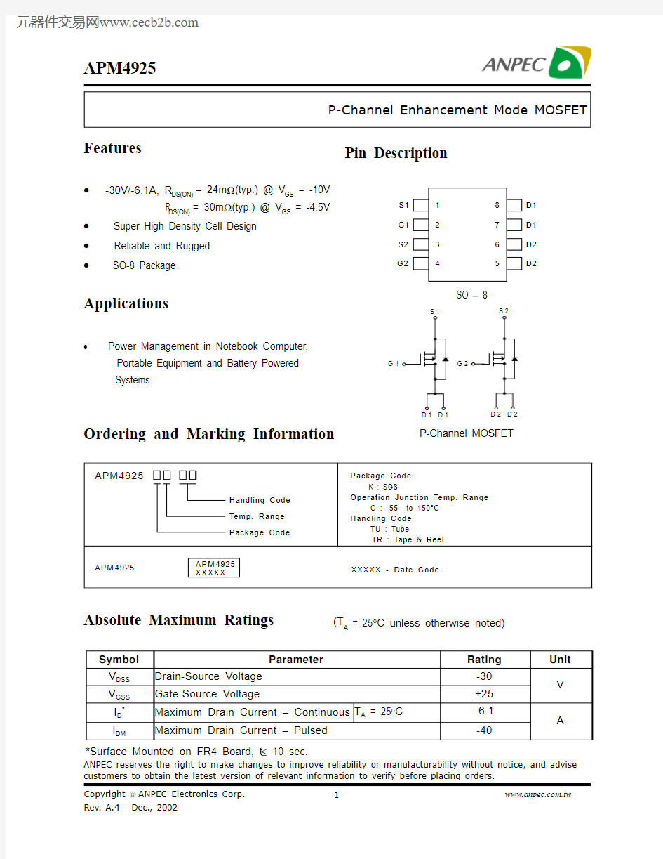
Pin Description
P-Channel MOSFET
S1G1S2G2
D2
D2D1D1G 1
G 2
SO ? 8
Notes
a : Guaranteed by design, not subject to production testing b
: Pulse test ; pulse width ≤ 300μs, duty cycle ≤ 2%
Electrical Characteristics (T A =25°C unless otherwise noted)
Absolute Maximum Ratings (T A = 25°C unless otherwise noted)
-50
-250255075100125150
0.600.750.901.051.201.351.50
0510********
0.00
0.010.020.030.040.050.06
012345
10
20
30
40
50
Typical Characteristics
-I D -D r a i n C u r r e n t (A )
Transfer Characteristics
-V GS - Gate-to-Source Voltage (V)
Threshold Voltage vs. Junction T emperature
Tj - Junction T emperature (°C)-V G S (t h )-T h r e s h o l d V o l t a g e (V )(N o r m a l z
e d )
On-Resistance vs. Drain Current
-I D - Drain Current (A)
R D S (o n )-O n -R e s
i s t a n c e (?)
0246810
1020
30
4050
Output Characteristics
-I D -D r a i n C u r r e n t (A )
-V DS - Drain-to-Source Voltage (V)
2
3
4
5
6
7
8
9
10
010********
2
4
6
8
10
Typical Characteristics
-V GS - Gate-to-Source Voltage (V)
R D S (o n )-O n -R e s i s t a n c e (?)
On-Resistance vs. Gate-to-Source Voltage
-50
-250255075100125150
0.60.81.01.2
1.41.61.8
R D S (o n )-O n -R e s i s t a n c e (?)(N o r m a l i z e d )
On-Resistance vs. Junction Temperature
T J - Junction T emperature (°C)0612182430
900
1800
2700
3600
4500
-V DS - Drain-to-Source Voltage (V)
Capacitance
C a p a c i t a n c e (p F )
Gate Charge
Q G - Gate Charge (nC)-V G S -G a t e -S o u r c e V o l t a g e (V )
1E-4
1E-30.010.1110
0.010.1
1
0.01
0.1110
020
40
60
80
100
Typical Characteristics
Single Pulse Power
Time (sec)
Square Wave Pulse Duration (sec)
N o r m a l i z e d E f f e c t i v e T r a n s i e n t T h e r m a l I m p e d a n c e
Normalized Thermal Transient Impedence, Junction to Ambient
0.0
0.20.40.60.8 1.0 1.2 1.4
0.110
P o w e r (W )
Source-Drain Diode Forward Voltage
-V SD -Source-to-Drain Voltage (V )
-I S -S o u r c e C u r r e n t (Α)
Package Information
SOP-8 pin ( Reference JEDEC Registration MS-012)
Physical Specifications
Reflow Condition (IR/Convection or VPR Reflow)
Reference JEDEC Standard J-STD-020A APRIL 1999
Classification Reflow Profiles
Package Reflow Conditions
Pre-heat temperature
183 C
Peak temperature
Time
°t e m p e r a t u r e
R e lia b ility te s t p ro g ra m
Carrier Tape
Cover Tape Dimensions
(mm) Customer Service
Anpec Electronics Corp.
Head Office :
5F, No. 2 Li-Hsin Road, SBIP,
Hsin-Chu, Taiwan, R.O.C.
T el : 886-3-5642000
Fax : 886-3-5642050
Taipei Branch :
7F, No. 137, Lane 235, Pac Chiao Rd.,
Hsin Tien City, Taipei Hsien, Taiwan, R. O. C.
T el : 886-2-89191368
Fax : 886-2-89191369