SKD420T
Absolute Maximum Ratings (T A =25°C unless otherwise noted)
Symbol Parameter Maximum Unit
V DSS Drain-to-Source Voltage 80 V
V GSS Gate-to-Source Voltage ±25 V
I D 3 Continuous Drain Current T C
=25°C 80 A
T C =100°C 70
I DP 4 Pulsed Drain Current
T C
=25°C 340
IAS 5
Avalanche Current
20 EAS 5
Avalanche energy
410 mJ
PD Maximum Power Dissipation T C =25°C 240
W
T C
=100°C 100
T J, T STG
Junction & Storage Temperature Range
-55~175 °C
Thermal Characteristics
Symbol Parameter
Typical Unit
R θjc Thermal Resistance-Junction to Case 0.52 ℃/W
R θja
Thermal Resistance-Junction to Ambient
55
? FEATURES
● 80V/80A
RDS(ON)= 9m ? (Max)@ VGS=10V ● Lead free and Green Device Available ● Low Rds-on to Minimize Conductive Loss ● High avalanche Current
? Application
● Power Supply ● DC-DC Converters
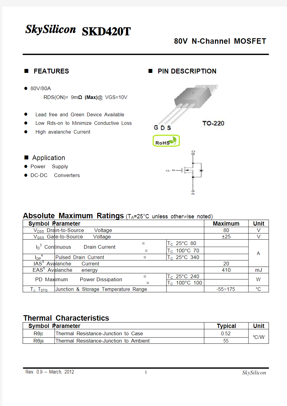
?PIN DESCRIPTION
Electrical Characteristics(TA=25°C unless otherwise noted)
Symbol Parameter Test
Conditions Min.
Typ
Max.Unit Static Characteristics
BV DSS Drain-Source Breakdown Voltage V GS=0V,I D
=250uA 80 — — V
I DSS Zero Gate Voltage Drain Current V DS=64V,V GS
=0V — — 1
uA T J
=125°C— — 100
V GS(th) Gate
Threshold
Voltage V DS=V GS,I D
=250uA 2 3 4 V I GSS Gate Leakage Current V GS=±25V, V DS
=0V — — ±100nA
R DS(on)1 Drain-Source
On-Resistance V GS=10V, I D
=40A — 7 9
m?
— — —
Diode Characteristics
V SD1Diode Forward Voltage I SD=40A,V GS
=0V — —
1.3
V
I S3Diode Continuous Forward Current — — 80 A
t rr Reverse
Recovery
Time I F=40A,
dI/dt=100A/us — 25 —nS
Q rr Reverse Recovery Charge — 18.5 —nC Dynamic Characteristics2
R G Gate
Resistance V GS=0V, V DS=0V,
Frequency=1MHz
— 1.3 — ?
C iss Input
Capacitance
V GS=0V, V DS=25V
Frequency=1MHz — 3110 —
pF
C oss Output
Capacitance — 445 —C rss Reverse
Transfer
Capacitance — 270 —
t d(on) Turn-On
Delay
Time
V DD=37.5V,I D=40A,
V GS=10V,R G=6.8?— 20.4 —
nS
t r Rise
Time — 63 —t d(off) Turn-Off
Delay
Time — 67 —t f Fall
Time — 43 —Gate Charge Characteristics2
Q g Total Gate Charge
V DS=37.5V,V GS=10V
I D=40A — 76 —
nC
Q gs Gate-to-Source
Charge — 9.5 —Q gd Gate-to-Drain
Charge — 40 —
Note: 1: Pulse test; pulse width ≦ 300us, duty cycle ≦ 2%.
2: Guaranteed by design, not subject to production testing.
3: Package limitation current is 50A.Calculated continuous current based on maximum allowable junction temperature.
4: Repetitive rating, pulse width limited by max junction temperature.
5: Starting TJ = 25°C,L = 1mH,IAS = 40A.
Typical Operating Characteristics
Typical Operating Characteristics
Typical Operating Characteristics
Typical Operating Characteristics