MAX4482ASA中文资料
For price, delivery, and to place orders,please contact Maxim Distribution at 1-888-629-4642,
or visit Maxim’s website at https://www.360docs.net/doc/ab12870932.html,.
General Description
The MAX4480–MAX4483 low-cost, general-purpose op amps offer Rail-to-Rail ?outputs, draw only 50μA of quies-cent current, and operate from a single +2.5V to +5.5V supply. For additional power conservation, the MAX4481offers a low-power shutdown mode that reduces supply current to 0.5μA (max) and puts the amplifier’s output in a high-impedance state. These devices are unity-gain sta-ble with capacitive loads up to 400pF. The MAX4480–MAX4483 are specified to +125°C, making them suitable for use in a variety of harsh environments, such as auto-motive applications.
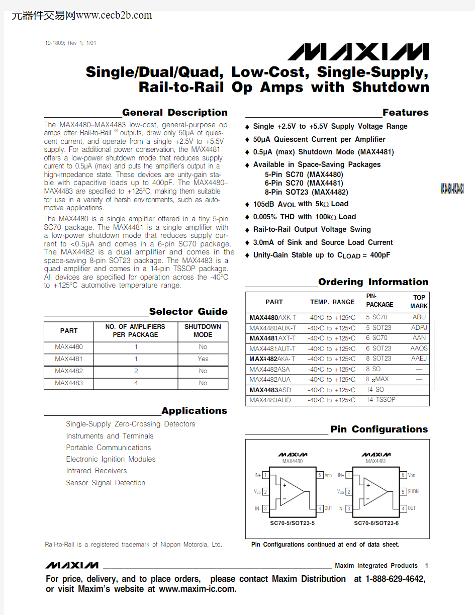
The MAX4480 is a single amplifier offered in a tiny 5-pin SC70 package. The MAX4481 is a single amplifier with a low-power shutdown mode that reduces supply cur-rent to <0.5μA and comes in a 6-pin SC70 package.The MAX4482 is a dual amplifier and comes in the space-saving 8-pin SOT23 package. The MAX4483 is a quad amplifier and comes in a 14-pin TSSOP package.All devices are specified for operation across the -40°C to +125°C automotive temperature range.
Applications
Single-Supply Zero-Crossing Detectors Instruments and Terminals Portable Communications Electronic Ignition Modules Infrared Receivers Sensor Signal Detection
Features
o Single +2.5V to +5.5V Supply Voltage Range o 50μA Quiescent Current per Amplifier o 0.5μA (max) Shutdown Mode (MAX4481)o Available in Space-Saving Packages
5-Pin SC70 (MAX4480)6-Pin SC70 (MAX4481)8-Pin SOT23 (MAX4482)o 105dB A VOL with 5k ?Load o 0.005% THD with 100k ?Load o Rail-to-Rail Output Voltage Swing o 3.0mA of Sink and Source Load Current o Unity-Gain Stable up to C LOAD = 400pF
MAX4480–MAX4483
Single/Dual/Quad, Low-Cost, Single-Supply,
Rail-to-Rail Op Amps with Shutdown
________________________________________________________________Maxim Integrated Products
1
19-1809; Rev 1; 1/01
Pin Configurations
Rail-to-Rail is a registered trademark of Nippon Motorola, Ltd.Pin Configurations continued at end of data sheet.
Ordering Information
M A X 4480–M A X 4483
Single/Dual/Quad, Low-Cost, Single-Supply,Rail-to-Rail Op Amps with Shutdown 2
_______________________________________________________________________________________
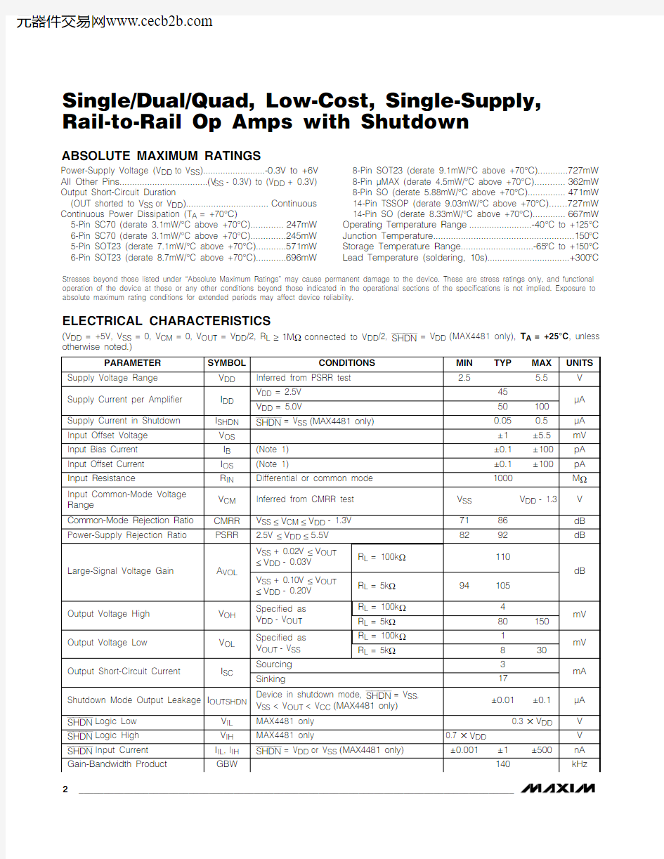
ABSOLUTE MAXIMUM RATINGS
ELECTRICAL CHARACTERISTICS
(V DD = +5V, V SS = 0, V CM = 0, V OUT = V DD /2, R L ≥1M ?connected to V DD /2, SHDN = V DD (MAX4481 only), T A = +25°C , unless otherwise noted.)
Stresses beyond those listed under “Absolute Maximum Ratings” may cause permanent damage to the device. These are stress ratings only, and functional operation of the device at these or any other conditions beyond those indicated in the operational sections of the specifications is not implied. Exposure to absolute maximum rating conditions for extended periods may affect device reliability.
Power-Supply Voltage (V DD to V SS ).........................-0.3V to +6V All Other Pins...................................(V SS - 0.3V) to (V DD + 0.3V)Output Short-Circuit Duration
(OUT shorted to V SS or V DD ).................................Continuous Continuous Power Dissipation (T A = +70°C)
5-Pin SC70 (derate 3.1mW/°C above +70°C).............247mW 6-Pin SC70 (derate 3.1mW/°C above +70°C)..............245mW 5-Pin SOT23 (derate 7.1mW/°C above +70°C)............571mW 6-Pin SOT23 (derate 8.7mW/°C above +70°C)............696mW
8-Pin SOT23 (derate 9.1mW/°C above +70°C)............727mW 8-Pin μMAX (derate 4.5mW/°C above +70°C)............362mW 8-Pin SO (derate 5.88mW/°C above +70°C)...............471mW 14-Pin TSSOP (derate 9.03mW/°C above +70°C).......727mW 14-Pin SO (derate 8.33mW/°C above +70°C).............667mW Operating Temperature Range .........................-40°C to +125°C Junction Temperature........................................................150°C Storage Temperature Range.............................-65°C to +150°C Lead Temperature (soldering, 10s).................................+300°C
MAX4480–MAX4483
Single/Dual/Quad, Low-Cost, Single-Supply,
Rail-to-Rail Op Amps with Shutdown
_______________________________________________________________________________________3
ELECTRICAL CHARACTERISTICS (continued)
(V DD = +5V, V SS = 0, V CM = 0, V OUT = V DD /2, R L ≥1M ?connected to V DD /2, SHDN = V DD (MAX4481 only), T A = +25°C , unless otherwise noted.)
(V DD = +5V, V SS = 0, V CM = 0, V OUT = V DD /2, R L ≥1M ?connected to V DD /2, SHDN = V DD (MAX4481 only), T A = -40°C to +125°C ,unless otherwise noted.) (Note 2)
Note 2:Specifications are 100% tested at T A = +25°C (exceptions noted). All temperature limits are guaranteed by design.
M A X 4480–M A X 4483
Single/Dual/Quad, Low-Cost, Single-Supply,Rail-to-Rail Op Amps with Shutdown 4_______________________________________________________________________________________
-100-120-140-160-180
1
10
1k
1M
100k
FREQUENCY (Hz)
100
10k
806040200-20-40-60-80GAIN AND PHASE vs. FREQUENCY (NO LOAD)
G A I N (d B )/P H A S E (d e g r e e s )
806040200-20-40-60-80-100-120-140-160-180
1
10
GAIN AND PHASE
vs. FREQUENCY (C L = 400pF)
FREQUENCY (Hz)
G A I N (d B )/P H A S E (d e g r e e s )
100
1k
1M
100k
10k
M A X 4480 t o c 03
10
1k
100
10k
100k
1M
POWER-SUPPLY REJECTION RATIO
vs. FREQUENCY
FREQUENCY (Hz)
P S R R (d B )10-110
-90
-10-30-50-70FREQUENCY (Hz)
10001
10
100
1k
10k
100k
OUTPUT IMPEDANCE vs. FREQUENCY
0.1M A X 4480 t o c 4
O U T P U T I M P E D A N C E (?)
100.01
1
1001M
40-400
40
80
-20
20
60
100120
SUPPLY CURRENT vs. TEMPERATURE
M A X 4480 t o c 05
TEMPERATURE (°C)
S U P P L Y C U R R E N T (μA )
42
44464850525456586010
-400
40
80
-20
20
60
100120
MAX4481
SHUTDOWN SUPPLY CURRENT
vs. TEMPERATURE
TEMPERATURE (°C)
S U P P L Y C U R R
E N T (p A )
11001k
10k 100k
-400
40
80
-20
20
60
100120
MAX4481
OUTPUT LEAKAGE CURRENT
vs. TEMPERATURE
TEMPERATURE (°C)
I L E A K
(p A )
101k
10k
100k
1000k
100-1500
-1000-500
500
10001500-400
40
80
-20
20
60
100120
INPUT OFFSET VOLTAGE vs. TEMPERATURE
TEMPERATURE (°C)
V O
S (μV )
80705040
90100-4004080-202060100120
OUTPUT VOLTAGE SWING HIGH
vs. TEMPERATURE
TEMPERATURE (°C)
V D D - V O U T (m V )
60Typical Operating Characteristics
(V DD = +5V, V SS = 0, V CM = V DD /2, V SHDN = 5V, R L ≥1M ?connected to V DD /2, T A = +25°C, unless otherwise noted.)
MAX4480–MAX4483
Single/Dual/Quad, Low-Cost, Single-Supply,
Rail-to-Rail Op Amps with Shutdown
_______________________________________________________________________________________5
47891011
-400
40
80
-20
20
60
100120
OUTPUT VOLTAGE SWING LOW
vs. TEMPERATURE
TEMPERATURE (°C)
V O U T - V S S (m V )
56
-90
-82
-80-400
40
80
-20
20
60
100120
COMMON-MODE REJECTION RATIO
vs. TEMPERATURE
M A X 4480 t o c 11
TEMPERATURE (°C)
C M R R (d B )
-88
-86
-8480105115
11085
120125130
0.5
1.5
2.5
3.5
1.0
2.0
3.0
4.0
4.5
LARGE-SIGNAL GAIN vs. OUTPUT VOLTAGE
V OUT (V)
G A I N (d B )
90100959095
100
105110
-400
40
80
-20
20
60
100120
LARGE-SIGNAL GAIN vs. TEMPERATURE
TEMPERATURE (°C)
G A I N (d B )
-400
40
80-20
20
60
100120
MINIMUM OPERATING VOLTAGE
vs. TEMPERATURE
M A X 4480 t o c 14
TEMPERATURE (°C)
V D D (M I N )
1.21.41.31.61.51.71.91.8
2.01.01.1
101k 10010k 100k
TOTAL HARMONIC DISTORTION PLUS NOISE vs. FREQUENCY
FREQUENCY (Hz)
T H D + N (%)
100
100.11
0.001
0.01
10
1k 100
10k
100k
TOTAL HARMONIC DISTORTION PLUS NOISE vs. FREQUENCY
FREQUENCY (Hz)
T H D + N (%)
100
0.001
101
0.01
0.1V IN (Vp-p)
T H D + N (%)
100
0.001
0.01
0.1110TOTAL HARMONIC DISTORTION PLUS NOISE vs. INPUT AMPLITUDE
2
1
3
0.001
0.01
1
0.1
10100
1.0
0.5
1.5
2.0
2.5
3.0
TOTAL HARMONIC DISTORTION PLUS NOISE vs. INPUT AMPLITUDE
V IN (Vp-p)
T H D + N (%)
Typical Operating Characteristics (continued)
(V DD = +5V, V SS = 0, V CM = V DD /2, V SHDN = 5V, R L ≥1M ?connected to V DD /2, T A = +25°C, unless otherwise noted.)
M A X 4480–M A X 4483
Single/Dual/Quad, Low-Cost, Single-Supply,Rail-to-Rail Op Amps with Shutdown 6_______________________________________________________________________________________
Typical Operating Characteristics (continued)
(V DD = +5V, V SS = 0, V CM = V DD /2, V SHDN = 5V, R L ≥1M ?connected to V DD /2, T A = +25°C, unless otherwise noted.)
CAPACITIVE-LOAD STABILITY
20
01k
10k
100k
5
RESISTIVE LOAD (?)
C A P A C I T I V E L O A
D (n F )
10
15
NONINVERTING SMALL-SIGNAL
TRANSIENT RESPONSE
20μs/div
A V = 1V/V R
L = 5k ?
IN
50mV/div
OUT
NONINVERTING LARGE-SIGNAL
TRANSIENT RESPONSE
100μs/div
A V = 1V/V R L = 5k ?
IN
1V/div
OUT
010
5
2015250
200
300100
400
500
600
PERCENT OVERSHOOT vs. CAPACITIVE LOAD
C LOA
D (pF)
O V E R S H O O T (%)
201040305060
0231456
SUPPLY CURRENT vs. SUPPLY VOLTAGE
SUPPLY VOLTAGE (V)
S U P P L Y C U R R E N T (μA )
2050408070601101009012010
1k
100
10k
100k
1M CHANNEL-TO-CHANNEL ISOLATION
vs. FREQUENCY
M A X 4480 t o c 23
FREQUENCY (kHz)C H A N N E L -T O -C H A N N E L I S O L A T I O N (d B )
30
MAX4480–MAX4483
Single/Dual/Quad, Low-Cost, Single-Supply,
Rail-to-Rail Op Amps with Shutdown
_______________________________________________________________________________________
7
Pin Description
Detailed Description
Rail-to-Rail Output Stage
The MAX4480–MAX4483 can drive a 5k ?load and still typically swing within 80mV of the supply rails. Figure 1shows the MAX4480 output voltage swing configured with A V = +10V/V.
Driving Capacitive Loads
Driving a capacitive load can cause instability in many op amps, especially those with low quiescent current.The MAX4480–MAX4483 are unity-gain stable for a range of capacitive loads to above 400pF. Figure 2shows the MAX4480 response with an excessive capacitive load. Adding a series resistor between the output and the load capacitor (Figure 3) improves the
1V/div
100μs/div
Figure 1. Rail-to-Rail Output Operation
MAX4483
MAX4482
MAX4480
MAX4481
IN+——1Noninverting Amplifier Input 1OUTC OUTD V DD SHDN
INC-IND-OUT OUTA OUTB V SS IN-INA-INB-IND+INC+INB+INA+NAME 8144—
913—1711—26121053PIN
——8—
———174—26——53Amplifier Output C ——Amplifier Output D
——Positive Supply. Use a 0.01μF bypass capacitor to GND.65Active-Low Shutdown Input. Connect to V DD for normal operation. Do not leave floating.
5
—
Inverting Amplifier Input C ——Inverting Amplifier Input D ——Amplifier Output 44Amplifier Output A ——Amplifier Output B ——Negative Supply. Connect to ground for single-supply operation. Use a 0.01μF bypass capacitor to GND.22Inverting Amplifier Input 33Inverting Amplifier Input A ——Inverting Amplifier Input B ——Noninverting Amplifier Input D
——Noninverting Amplifier Input C ——Noninverting Amplifier Input B ——Noninverting Amplifier Input A ——FUNCTION
M A X 4480–M A X 4483
Single/Dual/Quad, Low-Cost, Single-Supply,Rail-to-Rail Op Amps with Shutdown 8_______________________________________________________________________________________
circuit ’s response by isolating the load capacitance from the op amp ’s output.
Applications Information
Shutdown Mode
The MAX4481 features a low-power shutdown mode.When SHDN goes low, the supply current drops to 0.05μA (typ) and the output enters a high-impedance state. Pull SHDN high to enable the amplifier. Do not leave SHDN floating. Figure 4 shows the shutdown waveform.
Power-Up
The MAX4480–MAX4483 outputs typically settle within 50μs after power-up. Figure 5 shows the output voltage on power-up and power-down.
Power Supplies and Layout
The MAX4480–MAX4483 operate from a single +2.5V to +5.5V power supply. Bypass the power supply with a 0.1μF capacitor to ground.
Good layout techniques optimize performance by decreasing the amount of stray capacitance at the op amp ’s inputs and outputs. To decrease stray capaci-tance, minimize trace lengths by placing external com-ponents close to the op amp ’s pins.
Chip Information
MAX4480/MAX4481 TRANSISTOR COUNT: 111MAX4482 TRANSISTOR COUNT: 209MAX4483 TRANSISTOR COUNT: 407
20μs/div
C L = 1nF
Figure 3. Capacitive-Load-Driving Circuit
400μs/div
R L = 10M ? TO V SS , C L = 25pF
Figure 4. Shutdown Waveform 4μs/div
Figure 5. Power-Up/Down Waveform
Figure 2. Small-Signal Transient Response with Excessive Capacitive Load
MAX4480–MAX4483
Single/Dual/Quad, Low-Cost, Single-Supply,
Rail-to-Rail Op Amps with Shutdown
_______________________________________________________________________________________9
Pin Configurations (continued)
Package Information
M A X 4480–M A X 4483
Single/Dual/Quad, Low-Cost, Single-Supply,Rail-to-Rail Op Amps with Shutdown 10______________________________________________________________________________________
Package Information (continued)
MAX4480–MAX4483
Single/Dual/Quad, Low-Cost, Single-Supply,
Rail-to-Rail Op Amps with Shutdown
______________________________________________________________________________________
11
Package Information (continued)
Package Information (continued)
M A X 4480–M A X 4483
Single/Dual/Quad, Low-Cost, Single-Supply,Rail-to-Rail Op Amps with Shutdown 12______________________________________________________________________________________
Maxim c annot assume responsibility for use of any c irc uitry other than c irc uitry entirely embodied in a Maxim produc t. No c irc uit patent lic enses are implied. Maxim reserves the right to change the circuitry and specifications without notice at any time.
13____________________Maxim Integrated Products, 120 San Gabriel Drive, Sunnyvale, CA 94086 408-737-7600?2001 Maxim Integrated Products
Printed USA
is a registered trademark of Maxim Integrated Products.
Single/Dual/Quad, Low-Cost, Single-Supply,
Rail-to-Rail Op Amps with Shutdown
MAX4480–MAX4483
Package Information (continued)