EV4570-F-01A_r1.0
EV4570-F-01A
3A, 55V, Frequency Programmable
Step-Down Converter The Future of Analog IC Technology
DESCRIPTION
The EV4570-F-01A is an evaluation board for the MP4570/MPQ4570, a frequency programmable step-down switching converter with integrated internal high-side and low side power MOSFETs.
It can provide 3A continuous output current with peak current control for excellent transient response and efficiency performance.
The wide 4.5V to 55V input voltage range accommodates a variety of step down applications, including those applications in industrial, PoE, automotive and printer with DC high voltage bus.
The valley current detection is used to avoid current running way at over current protection. Also it has accurate and reliable over voltage protection, and auto recovery thermal protection.
In addition, the optional external soft start is available. Enable and power good indication function can be used to power track easily. In order to increase the efficiency, MP4570/MPQ4570 will automatically scaling down the switching frequency when load is light. Meanwhile, the low side MOSFET will be turned
off to reduce driver loss when zero inductor current is detected. Synchronous operation mode with integrated low side MOSFET is much helpful to reduce the conduction loss and also beneficial to reduce external components space and save the cost.
The MP4570/MPQ4570 is available in a TSSOP-
20 EP with exposed pad package. ELECTRICAL SPECIFICATIONS Parameter Symbol
Value
Units Input Voltage V IN 4.5-55 V
Output Voltage V OUT 3.3 V
Output Current I OUT 3 A FEATURES
?Wide Input Voltage Range: 4.5V to 55V ?Programmable Switching Frequency ?Stable Independent on Output Capacitors ?Optional External Soft Start
?Peak Current Mode Control
? OCP Protection with Valley Current Detection
?Support External SYNC Clock
? OVP Protection
?Current Limit Decreasing during Output Short for Better Thermal Performance ?Power Good Indication
?Thermal Shutdown Protection
?Fully Assembled and Tested APPLICATIONS
?PoE Input Non-isolated Buck
?Industrial Power Systems
?Printers and Scanners
? Automotive Power Systems
? Distributed Power Systems
All MPS parts are lead-free, halogen free, and adhere to the RoHS directive. For MPS green status, please visit MPS website under Quality Assurance. “MPS” and “The Future of Analog IC Technology” are Registered Trademarks of Monolithic Power Systems, Inc.
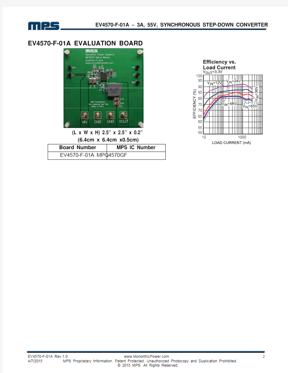
EV4570-F-01A EVALUATION BOARD
(L x W x H) 2.5” x 2.5” x 0.2” (6.4cm x 6.4cm x0.5cm)
Board Number MPS IC Number
EV4570-F-01A MPQ4570GF
EVALUATION BOARD SCHEMETIC
EN
GND
VOUT BIAS
EV4570-F-01A BILL OF MATERIALS
Qty Ref Value Description Package Manufacturer Part Number
2 C1A, C1B 2.2μF Ceramic
Capacitor;100V;X7R 1210 muRata GRM32ER72A225KA35L
1 C1C 0.1μF Ceramic
Capacitor;100V;X7R 0603 muRata GRM188R72A104KA35D
2 C2A,C2B 22μF
Ceramic
Capacitor;16V;X7R 1210 muRata GRM32ER71C226KE18L 2 C2C,C3 0.1μF Ceramic
Capacitor;16V;X7R 0603 muRata GRM188R71C104KA01D
1 C4 1nF
Ceramic
Capacitor;50V;X7R 0603 muRata GRM188R71H102KA01D 2 C5,C7 1μF Ceramic
Capacitor;16V;X7R 0603 muRata GRM188R71C105KA12D
1 C6 330pF
Ceramic
Capacitor;50V;C0G 0603 muRata GRM1885C1H331JA01D 1 C8 220pF
Ceramic
Capacitor;50V;C0G
0603 muRata GRM1885C1H221JA01D 1 C9 NS 1 R1 10k Film Resistor;1%; 0603 Yageo RC0603FR-0710KL 1 R2 4.32k Film Resistor;1%; 0603 Yageo RC0603FR-074K32L 1 R3 1M Film Resistor;5%; 0603 Yageo RC0603JR-071ML 1 R4 NS 1 R5 100k Film Resistor;1%; 0603 Yageo RC0603FR-07100KL 2 R6,R8 0 Film Resistor;5%; 0603 Yageo RC0603JR-070RL
EV4570-F-00A BILL OF MATERIALS (continued)
Qty Ref Value
Description Package Manufacturer
Part
Number
2 R7,R11 10 Film
Resistor;1%; 0603 Yageo RC0603FR-0710RL
1 R9 5.1k
Film
Resistor;1%; 0603 Yageo RC0603FR-075K1L
1 R10 102k
Film
Resistor;1%; 0603 Yageo RC0603FR-07102KL
1 D1 NS
1 L1 10μH Inductor;5.8A;25.4mohm
DCR
SMD ABC
CU1048100YEB Inductor;5.2A;30mohm DCR SMD Wurth 74437368100
1 U1 Synchronous Step-Down
Converter
TSSOP20MPS MPQ4570GF
4
VIN,
GND,
GND,
VOUT
2.0 Golden Pin HZ
11 PG,GND,
EN,GND,
BIAS
2.54mm Test Pin Any
V IN = 48V, V OUT =3.3V, C OUT = 2x22μF, L = 10μH, f SW=500kHz, T A = +25°C, unless otherwise noted.
V IN = 48V, V OUT =3.3V, C OUT = 2x22μF, L = 10μH, f SW=500kHz, T A = +25°C, unless otherwise noted.
V OUT
2V/div.
EN
2V/div.
I L
2A/div.
V OUT
2V/div.
SW
20V/div.
EN
2V/div.
I L
1A/div.
SW
20V/div.
V OUT
2V/div.
I L
1A/div.
SW
20V/div.
V OUT
2V/div.
I L
1A/div.
V OUT
1V/div.
I L
500mA/div.
SW
20V/div.
V OUT
2V/div.
I L
2A/div.
V OUT/AC
100mV/div.
I OUT
1A/div.
SW
20V/div.
V OUT
2V/div.
I L
2A/div.
EVB TEST RESULTS (continued)
V IN = 48V, V OUT =3.3V, C OUT = 2x22μF, L = 10μH, f SW =500kHz, T A = +25°C, unless otherwise noted.
V IN 5V/div.V OUT 1V/div.
V SW 10V/div.
I L 1A/div.V IN 5V/div.
V OUT 2V/div.
V SW 10V/div.
I L
1A/div.
PRINTED CIRCUIT LAYOUT
Figure1 – Top Silk Layer Figure 2 – Top Layer
Figure3 – Inner Layer 1Figure 4 – Inner Layer 2
Figure5 – Bottom Layer
NOTICE: The information in this document is subject to change without notice. Users should warrant and guarantee that third party Intellectual Property rights are not infringed upon when integrating MPS products into any application. MPS will not assume any legal responsibility for any said applications.
QUICK START GUIDE
1. Connect the positive and negative terminals of the load to the VOUT and GND pins respectively.
2. Preset the power supply output to between 4.5V to 55V, and then turn it off.
3. Connect the positive and negative terminals of the power supply output to the VIN and GND pins
respectively. 4. Turn the power supply on. The MP4570/MPQ4570GF will automatically startup.
5. To use the Enable function, apply a digital input to the EN pin. Drive EN higher than 1.6V to turn on
the regulator, drive EN less than 1.3V to turn it off. There is no internal pull-up or pull-down circuit, so do not float this pin. 6. Connection the EN pin directly to a voltage source without any pull-up resistors requires limiting
voltage amplitude to ≤6V to prevent damage to the internal zener diode between EN and GND; EN pin can also be connected to higher voltage (e.g. VIN) through pull-up resistor, but need to make sure the pull-up reisistor is high enough to make sure the sink current into EN pin less than 150μA to avoid damaging the zener diode. For example, when connecting EN to V IN =12V, R pull-up ≥ (12V – 6.5V) ÷ 150μA = 37k ?. 7. Use R10 to re-program switching frequency if needed. The recommended R FREQ values for various
f sw please see Table 1.
Table 1 — f SW vs. R FREQ
f SW (kHz)
R FREQ (k Ω)
1000 47.5 900 56 800 63.4 700 73.2 600 84.5 500 102 400 133 300 178 200 261 100 523
8. Use R1 and R2 to set the output voltage with V FB =1V. For R1=10k ?, R2 can be determined by:
k ?1
V 10R2OUT ?=
Follow the Application Information section in the device datasheet to recalculate the compensation, inductor and output capacitor values when output voltage is changed.