BC41B143A蓝牙芯片datasheet

_?ìé`?êé?QJolj=r?íê~íüá?=ti`pm= Product Data Sheet
_?ìé`?êé?QJolj=r?íê~íüá?=ti`pm Device Features Fully Qualified Bluetooth v2.0+EDR system Enhanced Data Rate (EDR) compliant with v2.0 of
specification for both 2Mbps and 3Mbps modulation modes Full Speed Bluetooth Operation with Full Piconet Support Scatternet Support
1.8V core, 1.7 to 3.6V I/O Split Rails
Ultra Low Power Consumption
Excellent Compatibility with Cellular Telephones
Minimum External Components Required
Integrated 1.8V Regulator
USB and UART Port to 3Mbits/s
Support for 802.11 Co-existence
RoHS Compliant
Low Profile Package
Single Chip Bluetooth ? v2.0 + EDR System
Pre-Production Information Data Sheet for BC41B143A February 2007General Description Applications
The _?ìé`?êé?QJolj=r?íê~íüá?=ti`pm is a
single-chip radio and baseband IC for Bluetooth 2.4GHz systems including EDR to 3Mbps. Cellular Handsets
Personal Digital Assistants
Digital cameras and other high-volume consumer products
Space-critical applications
With the on-chip CSR Bluetooth software stack it provides a fully compliant Bluetooth system to v2.0+EDR of the specification for data and voice communications.System Architecture
BlueCore4-ROM Ultrathin WLCSP is designed to
reduce the number of external components required.
This ensures that production costs are minimised.
The device incorporates auto-calibration and built in
self test (BIST) routines to simplify development, type
approval and production test. All hardware and device firmware is fully compliant with the Bluetooth v2.0+EDR Specification (all mandatory and optional features).
_?ìé`?êé?QJolj=r?íê~íüá?=ti`pm= Product Data Sheet
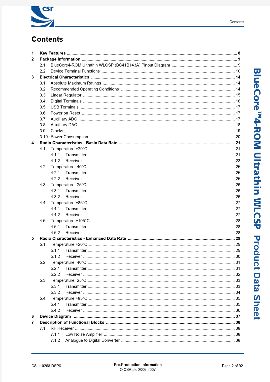
Contents
1Key Features (8)
2Package Information (9)
2.1BlueCore4-ROM Ultrathin WLCSP (BC41B143A) Pinout Diagram (9)
2.2Device Terminal Functions (10)
3Electrical Characteristics (14)
3.1Absolute Maximum Ratings (14)
3.2Recommended Operating Conditions (14)
3.3Linear Regulator (15)
3.4Digital Terminals (16)
3.5USB Terminals (17)
3.6Power on Reset (17)
3.7Auxilliary ADC (17)
3.8Auxilliary DAC (18)
3.9Clocks (19)
3.10Power Consumption (20)
4Radio Characteristics - Basic Data Rate (21)
4.1Temperature +20°C (21)
4.1.1Transmitter (21)
4.1.2Receiver (23)
4.2Temperature -40°C (25)
4.2.1Transmitter (25)
4.2.2Receiver (25)
4.3Temperature -25°C (26)
4.3.1Transmitter (26)
4.3.2Receiver (26)
4.4Temperature +85°C (27)
4.4.1Transmitter (27)
4.4.2Receiver (27)
4.5Temperature +105°C (28)
4.5.1Transmitter (28)
4.5.2Receiver (28)
5Radio Characteristics - Enhanced Data Rate (29)
5.1Temperature +20°C (29)
5.1.1Transmitter (29)
5.1.2Receiver (30)
5.2Temperature -40°C (31)
5.2.1Transmitter (31)
5.2.2Receiver (32)
5.3Temperature -25°C (33)
5.3.1Transmitter (33)
5.3.2Receiver (34)
5.4Temperature +85°C (35)
5.4.1Transmitter (35)
5.4.2Receiver (36)
6Device Diagram (37)
7Description of Functional Blocks (38)
7.1RF Receiver (38)
7.1.1Low Noise Amplifier (38)
7.1.2Analogue to Digital Converter (38)
_?ìé`?êé?QJolj=r?íê~íüá?=ti`pm= Product Data Sheet
7.2RF Transmitter (38)
7.2.1IQ Modulator (38)
7.2.2Power Amplifier (38)
7.2.3Auxiliary DAC (38)
7.3RF Synthesiser (38)
7.4Power Control and Regulation (38)
7.5Clock Input and Generation (38)
7.6Baseband and Logic (39)
7.6.1Memory Management Unit (39)
7.6.2Burst Mode Controller (39)
7.6.3Physical Layer Hardware Engine DSP (39)
7.6.4System RAM (39)
7.6.5ROM (39)
7.6.6USB (39)
7.6.7Synchronous Serial Interface (39)
7.6.8UART (39)
7.6.9Audio PCM Interface (39)
7.7Microcontroller (40)
7.7.1Programmable I/O (40)
7.7.2802.11 Co-Existence Interface (40)
8CSR Bluetooth Software Stacks (41)
8.1BlueCore HCI Stack (41)
8.1.1Key Features of the HCI Stack: Standard Bluetooth Functionality (42)
8.1.2Key Features of the HCI Stack: Extra Functionality (43)
8.2BCHS Software (44)
8.3Additional Software for Other Embedded Applications (44)
8.4CSR Development Systems (44)
9Device Terminal Descriptions (45)
9.1RF Ports (45)
9.1.1RF_A and RF_B (45)
9.1.2Transmit RF Power Control for Class 1 Applications (TX_PWR) (46)
9.1.3Control of External RF Components (47)
9.2External Reference Clock Input (XTAL_IN) (47)
9.2.1External Mode (47)
9.2.2XTAL_IN Impedance in External Mode (47)
9.2.3Clock Timing Accuracy (48)
9.2.4Clock Start-Up Delay (49)
9.2.5Input Frequencies and PS Key Settings (50)
9.3Crystal Oscillator (XTAL_IN, XTAL_OUT) (50)
9.3.1XTAL Mode (50)
9.3.2Load Capacitance (52)
9.3.3Frequency Trim (53)
9.3.4Transconductance Driver Model (54)
9.3.5Negative Resistance Model (54)
9.3.6Crystal PS Key Settings (55)
9.3.7Crystal Oscillator Characteristics (55)
9.4UART Interface (57)
9.4.1UART Bypass (60)
9.4.2UART Configuration While RESET is Active (60)
9.4.3UART Bypass Mode (60)
9.4.4Current Consumption in UART Bypass Mode (60)
9.5USB Interface (60)
_?ìé`?êé?QJolj=r?íê~íüá?=ti`pm= Product Data Sheet
9.5.1USB Data Connections (61)
9.5.2USB Pull-Up Resistor (61)
9.5.3USB Power Supply (61)
9.5.4Self-Powered Mode (62)
9.5.5Bus-Powered Mode (62)
9.5.6Suspend Current (63)
9.5.7Detach and Wake_Up Signalling (63)
9.5.8USB Driver (64)
9.5.9USB 1.1 Compliance (64)
9.5.10USB 2.0 Compatibility (64)
9.6Serial Peripheral Interface (65)
9.6.1Instruction Cycle (65)
9.6.2Writing to the Device (66)
9.6.3Reading from the Device (66)
9.6.4Multi-Slave Operation (66)
9.7I/O Parallel Ports (67)
9.7.1PIO Defaults (67)
9.8I2C Master (67)
9.9TCXO Enable OR Function (68)
9.10RESETB (69)
9.10.1Pin States on Reset (70)
9.10.2Status after Reset (70)
9.11PCM CODEC Interface (71)
9.11.1PCM Interface Master/Slave (71)
9.11.2Long Frame Sync (72)
9.11.3Short Frame Sync (72)
9.11.4Multi-slot Operation (73)
9.11.5GCI Interface (73)
9.11.6Slots and Sample Formats (74)
9.11.7Additional Features (75)
9.11.8PCM Timing Information (76)
9.11.9PCM Configuration (79)
9.12Power Supply (81)
9.12.1Voltage Regulator (81)
9.12.2Sequencing (81)
9.12.3Sensitivity to Disturbances (81)
10Application Schematic (82)
11Package Dimensions (83)
12PCB Design and Assembly Considerations (84)
12.1 3.8 x 4.0 x 0.35mm Ultrathin WLCSP 47-Bump Package (84)
13Solder Profiles (85)
13.1Typical Solder Re-flow Profile for Devices with Lead-Free Solder Balls (85)
14RoHS Statement with a List of Banned Materials (86)
14.1RoHS Statement (86)
14.1.1List of Banned Materials (86)
15Ordering Information (87)
15.1BlueCore4-ROM Ultrathin WLCSP (87)
16Document References (88)
17Terms and Definitions (89)
18Document History (92)
_?ìé`?êé?QJolj=r?íê~íüá?=ti`pm= Product Data Sheet
List of Figures
Figure 2.1BlueCore4-ROM Ultrathin WLCSP Package (9)
Figure 6.1BlueCore4-ROM Ultrathin WLCSP Device Diagram (37)
Figure 8.1BlueCore HCI Stack (41)
Figure 9.1Circuit TX/RF_A and TX/RF_B (45)
Figure 9.2TCXO Clock Accuracy (48)
Figure 9.3Crystal Driver Circuit (51)
Figure 9.4Crystal Equivalent Circuit (51)
Figure 9.5Crystal Load Capacitance and Series Resistance Limits with Crystal Frequency (55)
Figure 9.6Crystal Driver Transconductance vs. Driver Level Register Setting (56)
Figure 9.7Crystal Driver Negative Resistance as a Function of Drive Level Setting (57)
Figure 9.8Universal Asynchronous Receiver (58)
Figure 9.9Break Signal (58)
Figure 9.10UART Bypass Architecture (60)
Figure 9.11USB Connections for Self-Powered Mode (62)
Figure 9.12USB Connections for Bus-Powered Mode (63)
Figure 9.13USB_DETACH and USB_WAKE_UP Signal (64)
Figure 9.14SPI Write Operation (66)
Figure 9.15SPI Read Operation (66)
Figure 9.16Example EEPROM Connection (67)
Figure 9.17Example TCXO Enable OR Function (68)
Figure 9.18BlueCore4-ROM Ultrathin WLCSP as PCM Interface Master (71)
Figure 9.19BlueCore4-ROM Ultrathin WLCSP as PCM Interface Slave (72)
Figure 9.20Long Frame Sync (Shown with 8-bit Companded Sample) (72)
Figure 9.21Short Frame Sync (Shown with 16-bit Sample)..........................................................................73Figure 9.22Multi-slot Operation with Two Slots and 8-bit Companded Samples (73)
Figure 9.23GCI Interface (74)
Figure 9.2416-Bit Slot Length and Sample Formats (75)
Figure 9.25PCM Master Timing Long Frame Sync (77)
Figure 9.26PCM Master Timing Short Frame Sync (77)
Figure 9.27PCM Slave Timing Long Frame Sync (78)
Figure 9.28PCM Slave Timing Short Frame Sync (79)
Figure 10.1Application Circuit for Radio Characteristics Specification (82)
Figure 11.1BlueCore4-ROM Ultrathin WLCSP Package Dimensions (83)
Figure 13.1Typical Lead-Free Re-flow Solder Profile...................................................................................85List of Tables
Table 9.1TXRX_PIO_CONTROL Values (47)
Table 9.2External Clock Specifications (47)
Table 9.3PS Key Values for CDMA/3G Phone TCXO Frequencies (50)
Table 9.4Crystal Specification (52)
Table 9.5Possible UART Settings (58)
Table 9.6Standard Data Rates (59)
Table 9.7USB Interface Component Values (62)
Table 9.8Instruction Cycle for an SPI Transaction (65)
Table 9.9Pin States of BlueCore4-ROM Ultrathin WLCSP on Reset (70)
Table 9.10PCM Master Timing (76)
Table 9.11PCM Slave Timing (78)
Table 9.12PSKEY_PCM_CONFIG32 Description (81)
Table 9.13PSKEY_PCM_LOW_JITTER_CONFIG Description (81)
_?ìé`?êé?QJolj=r?íê~íüá?=ti`pm= Product Data Sheet
List of Equations
Equation 9.1Output Voltage with Load Current ≤ 10mA (46)
Equation 9.2Output Voltage with No Load Current (46)
Equation 9.3Internal Power Ramping (46)
Equation 9.4Load Capacitance (52)
Equation 9.5Trim Capacitance (53)
Equation 9.6Frequency Trim (53)
Equation 9.7Pullability (53)
Equation 9.8Transconductance Required for Oscillation (54)
Equation 9.9Equivalent Negative Resistance (54)
Equation 9.10Data Rate (59)
Equation 9.11PCM_CLK Frequency When Being Generated Using the Internal 48MHz Clock (79)
Equation 9.12PCM_SYNC Frequency Relative to PCM_CLK (79)
Status Information
_?ìé`?êé?QJolj=r?íê~íüá?=ti`pm= Product Data Sheet
Status Information
The status of this Data Sheet is Pre-Production Information .
CSR Product Data Sheets progress according to the following format:
Advance Information
Information for designers concerning CSR product in development. All values specified are the target values of the design. Minimum and maximum values specified are only given as guidance to the final specification limits and must not be considered as the final values.
All detailed specifications including pinouts and electrical specifications may be changed by CSR without notice.Pre-Production Information
Pinout and mechanical dimension specifications finalised. All values specified are the target values of the design. Minimum and maximum values specified are only given as guidance to the final specification limits and must not be considered as the final values.
All electrical specifications may be changed by CSR without notice.
Production Information
Final Data Sheet including the guaranteed minimum and maximum limits for the electrical specifications.
Production Data Sheets supersede all previous document versions.
Life Support Policy and Use in Safety-Critical Applications
CSR's products are not authorised for use in life-support or safety-critical applications. Use in such applications is done at the sole discretion of the customer. CSR will not warrant the use of its devices in such applications.
Trademarks, Patents and Licenses
Unless otherwise stated, words and logos marked with ? or ? are trademarks registered or owned by CSR plc or its affiliates. Bluetooth ? and the Bluetooth logos are trademarks owned by Bluetooth SIG, Inc. and licensed to CSR. Other products, services and names used in this document may have been trademarked by their respective owners.
The publication of this information does not imply that any license is granted under any patent or other rights owned by CSR plc.
CSR reserves the right to make technical changes to its products as part of its development programme.
While every care has been taken to ensure the accuracy of the contents of this document, CSR cannot accept responsibility for any errors.
Key Features
_?ìé`?êé?QJolj=r?íê~íüá?=ti`pm= Product Data Sheet
1Key Features
Radio Common TX/RX terminals simplify external matching and eliminates external antenna switch BIST minimises production test time. No external trimming is required in production Full RF reference designs are available Bluetooth v2.0+EDR specification compliant Transmitter +6dBm RF transmit power with level control from on-chip 6-bit DAC over a dynamic range >30dB Class 2 and Class 3 support without the need for an external power amplifier or TX/RX switch Class1 support using external power amplifier with RF power controlled by an internal 8-bit DAC Supports DQPSK (2Mbps) and 8DPSK (3Mbps) modulation Receiver Integrated channel filters Digital demodulator for improved sensitivity and
co-channel rejection Real-time digitised RSSI available on HCI interface Fast AGC for enhanced dynamic range Supports DQPSK and 8DPSK modulation Channel classification Synthesiser Fully integrated synthesiser requires no external VCO varactor diode, resonator or loop filter Compatible with crystals between 8 and 40MHz (in multiples of 250kHz) or an external clock Accepts 7.68, 14.4, 15.36, 16.2, 16.8, 19.2, 19.44,
19.68, 19.8 and 38.4MHz TCXO frequencies for GSM and CDMA devices with sinusoidal or logic level signals Auxiliary Features Crystal oscillator with built-in digital trimming Power management includes digital shutdown, and wake up commands with an integrated low-power oscillator for ultra low Park/Sniff/Hold mode
Clock request output to control external clock
Auxilliary Features (Continued)
Device can run in low power modes from an external
32kHz clock signal
Auto Baud Rate setting for different TCXO
frequencies
On-chip linear regulator, producing 1.8V output from 2.2-5.6V input
Power-on-reset cell detects low supply voltage Baseband and Software
Internal 48-KByte RAM, allows full-speed data
transfer, mixed voice and data, and full piconet
operation, including all medium rate preset types Logic for forward error correction, header error
control, access code correlation, CRC, demodulation, encryption bit stream generation, whitening and
transmit pulse shaping. Supports all Bluetooth v2.0 +
EDR features including eSCO and AFH
Transcoders for A-law, μ-law and linear voice from host and A-law, μ-law and CVSD voice over air Physical Interfaces
Synchronous serial interface up to 4Mbit/s for system debugging
UART interface with programmable baud rate up to
3Mbits/s with an optional bypass mode Full-speed USB v2.0 interface supports OHCI and UHCI host interfaces
Synchronous bi-directional serial programmable
audio interface
Optional I 2C? compatible interface
Optional 802.11 co-existence interfaces
Bluetooth Stack
CSR's Bluetooth Protocol Stack runs on the on-chip MCU in a variety of configurations:
Standard HCI (UART or USB)
Customised builds with embedded application code Package Options
47-Bump WLCSP 3.8 x 4.0 x 0.35mm
_?ìé`?êé?QJolj=r?íê~íüá?=ti`pm= Product Data Sheet
2Package Information
2.1BlueCore4-ROM Ultrathin WLCSP (BC41B143A) Pinout Diagram
Figure 2.1: BlueCore4-ROM Ultrathin WLCSP Package
A B C D E F G 1234567
A2A3A4A5A6A7
B1B2B3B4B5B6B7
C1C2C3C4C5C6C7
D2D3E1E2E3F1F2F3G1G2G3D5D6D7
E5E6E7
F5F6F7
G5G6G7
D4E4F4G4Orientation from top of device
_?ìé`?êé?QJolj=r?íê~íüá?=ti`pm= Product Data Sheet
2.2Device Terminal Functions
Radio Bump Pad Type Description
RF_A E2Analogue Transmitter output/switched
receiver input
RF_B E1Analogue Complement of RF_A
AUX_DAC D2Analogue Voltage DAC
Synthesiser and Oscillator Bump Pad Type Description
XTAL_IN A3Analogue For crystal or external clock input XTAL_OUT B3Analogue Drive for crystal
PCM Interface Bump Pad Type Description
PCM_OUT E4CMOS output, tri-state, with weak
internal pull-down Synchronous data output
PCM_IN B7CMOS input, with weak internal
pull-down Synchronous data input
PCM_SYNC D5Bi-directional with weak internal
pull-down Synchronous data sync
PCM_CLK B6Bi-directional with weak internal
pull-down Synchronous data clock
_?ìé`?êé?QJolj=r?íê~íüá?=ti`pm= Product Data Sheet
USB and UART Bump Pad Type Description
UART_TX C5CMOS output, tri-statable with
weak internal pull-up UART data output active high
UART_RX D4CMOS input with weak internal
pull-down UART data input active high
UART_RTS A7CMOS output, tri-statable with
weak internal pull-up UART request to send active low
UART_CTS C4CMOS input with weak internal
pull-down USB clear to send active low
USB_DP B5Bi-directional USB data plus with selectable
internal 1.5? pull-up resistor
USB_DN A6Bi-directional USB data minus
_?ìé`?êé?QJolj=r?íê~íüá?=ti`pm= Product Data Sheet
PIO Port Bump Pad Type Description
PIO[0]F3Bi-directional with programmable
strength internal pull-up/down Programmable input/output line
PIO[1]F4Bi-directional with programmable
strength internal pull-up/down Programmable input/output line
PIO[2]G1Bi-directional with programmable
strength internal pull-up/down Programmable input/output line
PIO[3]G2Bi-directional with programmable
strength internal pull-up/down Programmable input/output line
PIO[4]E6Bi-directional with programmable
strength internal pull-up/down Programmable input/output line
PIO[5]F5Bi-directional with programmable
strength internal pull-up/down Programmable input/output line
PIO[6]D7Bi-directional with programmable
strength internal pull-up/down Programmable input/output line
PIO[7]E5Bi-directional with programmable
strength internal pull-up/down Programmable input/output line
PIO[8]E3Bi-directional with programmable
strength internal pull-up/down Programmable input/output line
PIO[9]F1Bi-directional with programmable
strength internal pull-up/down Programmable input/output line
PIO[10]F2Bi-directional with programmable
strength internal pull-up/down Programmable input/output line
AIO[0]D3Bi-directional Programmable input/output line AIO[2]C3Bi-directional Programmable input/output line
_?ìé`?êé?QJolj=r?íê~íüá?=ti`pm= Product Data Sheet Power Supplies and
Control Bump Pad Type Description
VREG_IN A2Regulator input Regulator input
VDD_USB A5VDD Positive supply for UART ports and AIOs VDD_PIO G4VDD Positive supply for PIO [3:0] and [10:8] VDD_PADS D6VDD Positive supply for all digital Input/Output
ports and PIO[7:4]
VDD_CORE C6VDD Positive supply for internal digital
circuitry
VDD_LO B2VDD Positive supply for VCO and synthesiser
circuitry
VDD_RADIO C2VDD Positive supply for RF circuitry
VDD_ANA A4VDD/Regulator output Positive supply for analogue circuitry
and 1.8V regulated output
VSS_DIG C7VSS Ground connection for internal digital
circuitry and digital ports
VSS_PADS G3VSS Ground connection for digital ports VSS_RADIO C1VSS Ground connections for RF circuitry VSS_ANA B4VSS Ground connections for analogue
circuitry
VSS_LO B1VSS Ground connection for VCO and
synthesiser circuitry
_?ìé`?êé?QJolj=r?íê~íüá?=ti`pm= Product Data Sheet
3Electrical Characteristics
3.1Absolute Maximum Ratings
3.2Recommended Operating Conditions
(a)Typical figures are given for RF performance between -40°C and +105°C (b)The device will operate without damage with VREG_IN as high as 5.6V, however the RF performance is not guaranteed
above 4.2V
Rating Min Max
Storage Temperature -40°C +150°C
Supply Voltage: VDD_RADIO, VDD_LO, VDD_ANA and
VDD_CORE -0.4V 2.2V
Supply Voltage: VDD_PADS, VDD_PIO and VDD_USB -0.4V 3.7V
Supply Voltage: VREG_IN -0.4V 5.6V
Other Terminal Voltages VSS-0.4V VDD+0.4V
Operating Condition Min Max
Operating Temperature Range -40°C +105°C
Guaranteed RF performance range (a) -40°C +85°C
Supply Voltage: VDD_RADIO, VDD_LO, VDD_ANA and
VDD_CORE 1.7V 1.9V
Supply Voltage: VDD_PADS, VDD_PIO and VDD_USB 1.7V 3.6V
Supply Voltage: VREG_IN 2.2V 4.2V (b)
_?ìé`?êé?QJolj=r?íê~íüá?=ti`pm= Product Data Sheet
3.3Linear Regulator
(a)Regulator output connected to 47nF pure and 4.7μF 2.2? ESR capacitors
(b)Frequency range is 100Hz to 100kHz (c)1mA to 70mA pulsed load (d)Operation up to 5.6V is permissible without damage and without the output voltage rising sufficiently to damage the rest
of BlueCore4-ROM Ultrathin WLCSP , but output regulation and other specifications are no longer guaranteed at input
voltages in excess of 4.2V
(e)Low power mode is entered and exited automatically when the chip enters/leaves Deep Sleep mode
(f)Regulator is disabled when VREG_IN is either open circuit or driven to the same voltage as VDD_ANA Linear Regulator Min Typ Max Unit Normal Operation
Output voltage (I load = 70 mA / VREG_IN = 3.0V)) 1.70 1.78 1.85V Temperature coefficient -250-250ppm/°C Output noise (a) (b) --1mV rms Load regulation (I load < 70 mA)--50mV/A Settling Time (a) (c) --50μs Maximum output current 70--mA Minimum load current 5--μA Input voltage -- 4.2(d) V Dropout voltage (I load = 70 mA)--350mV Quiescent current (excluding Ioad, I load < 1mA)253550μA Low Power Mode (e)
Quiescent current (excluding Ioad, I load < 100μA)4710μA Disabled Mode (f)
Quiescent Current 1.5 2.5 3.5μA
_?ìé`?êé?QJolj=r?íê~íüá?=ti`pm= Product Data Sheet
3.4Digital Terminals
(a)Current sunk into terminal
(b)Current sourced out of terminal
Digital Terminals Min Typ Max Unit Input Voltage Levels
V IL input logic level low 2.7V ≤ VDD ≤ 3.0V -0.4-+0.8V 1.7V ≤ VDD ≤ 1.9V -0.4-+0.4V V IH input logic level high 0.7VDD -VDD+0.4V Output Voltage Levels
V OL output logic level low,
--0.2V (l o = 4.0mA)(a) , 2.7V ≤ VDD ≤ 3.0V
V OL output logic level low,
--0.4V (l o = 4.0mA)(a) , 1.7V ≤ VDD ≤ 1.9V
V OH output logic level high,
VDD-0.2--V (l o = -4.0mA)(b) , 2.7V ≤ VDD ≤ 3.0V
V OH output logic level high,
VDD-0.4--V (l o = -4.0mA)(b) , 1.7V ≤ VDD ≤ 1.9V
Input and Tri-state Current with:
Strong pull-up -100-40-10μA Strong pull-down 1040100μA Weak pull-up -5.0-1.0-0.2μA
Weak pull-down 0.2 1.0 5.0μA I/O pad leakage current -10+1μA C I input capacitance 1.0- 5.0pF
_?ìé`?êé?QJolj=r?íê~íüá?=ti`pm= Product Data Sheet
3.5USB Terminals
(a)Internal USB pull-up disabled
3.6Power on Reset
3.7Auxilliary ADC
(a)ADC is accessed through the VM function. The sample rate given is achieved as part of this function
USB Terminals Min Typ Max Unit VDD_USB for correct USB operation 3.1 3.6V Input Threshold
V IL input logic level low --0.3VDD_USB V V IH input logic level high 0.7VDD_USB --V Input Leakage Current
VSS_PADS < VIN < VDD_USB (a) -115μA C I Input capacitance 2.5-10.0pF Output Voltage Levels to Correctly Terminated
USB Cable
V OL output logic level low 0.0-0.2V V OH output logic level high 2.8-VDD_USB V
Power-on Reset Min Typ Max Unit VDD_CORE falling threshold 1.40 1.50 1.60V VDD_CORE rising threshold 1.50 1.60 1.70V
Hysteresis 0.050.100.15V
Auxiliary ADC Min Typ Max Unit Resolution --8Bits Input voltage range
0-VDD_ANA V (LSB size = VDD_ANA/255)Accuracy INL -1-1LSB (Guaranteed monotonic)DNL 0-1LSB Offset -1-1LSB Gain Error -0.8-0.8%Input Bandwidth -100-kHz Conversion time - 2.5-μs Sample rate (a) --700Samples/s
_?ìé`?êé?QJolj=r?íê~íüá?=ti`pm= Product Data Sheet
3.8Auxilliary DAC
(a)Specified for an output voltage between 0.2V and VDD_PIO -0.2V. Output is high impedance when chip is in Deep Sleep
mode Auxiliary DAC Min Typ Max Unit Resolution --8Bits Average output step size (a) 12.514.517.0mV Output Voltage monotonic (a)
Voltage range (I O =0mA)VSS_PADS -VDD_PIO V Current range -10.0-0.1mA Minimum output voltage (I O =100μA)0.0-0.2V Maximum output voltage (I O =10mA)VDD_PIO-0.3-VDD_PIO V High Impedance leakage current -1-1μA Offset -220-120mV Integral non-linearity (a) -2-2LSB Settling time (50pF load)--10μs
_?ìé`?êé?QJolj=r?íê~íüá?=ti`pm= Product Data Sheet
3.9Clocks
(a)Integer multiple of 250kHz (b)The difference between the internal capacitance at minimum and maximum settings of the internal digital trim.
(c)XTAL frequency = 16MHz; XTAL C0 = 0.75pF; XTAL load capacitance = 8.5pF.
(d)Clock input can be any frequency between 8MHz and 40MHz in steps of 250kHz plus CDMA/3G TCXO frequencies of
7.68, 14.44, 15.36, 16.2, 16.8, 19.2, 19.44, 19.68, 19.8 and 38.4MHz.
(e)Clock input can be either sinusoidal or square wave. If the peaks of the signal are below VSS_ANA or above VDD_ANA.
A DC blocking capacitor is required between the signal and XTAL_IN.
Notes:VDD_CORE, VDD_RADIO, VDD_LO and VDD_ANA are at 1.8V unless shown otherwise.
VDD_PADS, VDD_PIO and VDD_USB are at 3.15V unless shown otherwise.
The same setting of the digital trim is applied to both XTAL_IN and XTAL_OUT.
Current drawn into a pin is defined as positive; current supplied out of a pin is defined as negative.Crystal Oscillator Min Typ Max Unit Crystal frequency (a) 8.0-40.0MHz Digital trim range (b) 5.0 6.28.0pF Trim step size (b) -0.1-pF Transconductance 2.0--mS Negative resistance (c) 87015002400?External Clock
Input frequency (d) 8.0-40.0MHz Clock input level (e) 0.4-VDD_ANA V pk-pk Allowable Jitter --15ps rms XTAL_IN input impedance -≥10-k ?XTAL_IN input capacitance - ≤ 4-pF
_?ìé`?êé?QJolj=r?íê~íüá?=ti`pm= Product Data Sheet 3.10Power Consumption
(a)Low power mode on the linear regulator is entered and exited automatically when the chip enters/leaves Deep Sleep
mode. For more information about the electrical characteristics of the linear regulator, see section 3.3 in this document.
Note:
Conditions: 20°C, VREG_IN 3.15V linear regulator supplying 1.8V
Operation Mode Connection Type UART Rate (kbps)Average Unit
Page scan, time
interval 1.28s -115.20.41mA
Inquiry and page scan -115.20.77mA
ACL No traffic Master 115.2 6.4mA
ACL With file transfer Master 115.211mA
ACL No traffic Slave 115.214mA
ACL With file transfer Slave 115.217mA
ACL 40ms sniff Master 38.4 1.5mA
ACL 1.28s sniff Master 38.40.19mA
SCO HV1Master 38.434mA
SCO HV3Master 38.417mA
SCO HV3 30ms sniff Master 38.417mA
ACL 40ms sniff Slave 38.4 1.5mA
ACL 1.28s sniff Slave 38.40.24mA
Parked 1.28s beacon Slave 38.40.18mA
SCO HV1Slave 38.434mA
SCO HV3Slave 38.421mA
SCO HV3 30ms sniff Slave 38.417mA
Standby Host
connection -38.40.03mA
(Deep Sleep)(a)
Reset (RESETB low)(a) --0.04mA
IC-HK_datasheet
Rev 21.11.01, Page 1/13 current of 100mA pulse current of 100mA Fig. 2: Signal patterns for Example 1 -pulse current of 100mA APPLICATION NOTES Setting the laser current When switching DC currents of up to 150mA or pulse currents of up to 700mA one channel is sufficient (Example 1). Input ENx of the unused channel should be jumpered to GND and pin AGNDx left open. Higher currents or several different current levels can be obtained by using both channels (Example 2 and 3).Example 1:Switching a current of 100mA 1. 100mA < 150mA | one channel 2. Switching on and off only | RK can be omitted (RK = 0S ) 3. As shown in Figure 1 (cf. data sheet, Figures 2..4), the required voltage V(CI) for RK = 0S is read off at I(LDK) = 100mA as V(CI) =1.75V With the circuit shown in Figure 3 and a voltage of 1.75V at pin CI the laser current can be switched between typically 0mA and 100mA by applying an appropriate pulse pattern to EN1.
芯片数据手册Datasheet热门问题
芯片数据手册Datasheet热门问题 ?如何正确的阅读Datasheet? 不仅仅是芯片,包括工具、设备几乎任何电子产品,都需要去阅读它的datasheet,除了包括最低、最高要求,特点,建议和用途及其兼容的设备等等,更重要的是原厂商以一个成功者的身份去告诉你一些注意事项。 Datasheet一般组成的字段:(LM317举例) ①日期:首先检查发布日期,是预备版还是修正版 ②厂商:检查厂商,因为相同型号不同厂商的器件,性能或许不同 ③描述(Description):往往会告诉你一些一般地方没有提到的功能或者用法。比如:你可能需要保持一个特殊的引脚为低电平才能完成某个操作。 ④特点(Features):告诉你常规特征。确认电器特征相应的条件 ⑤应用(Application):通常简洁的告诉你该器件是否在你的应用领域;如果这个芯片有你需要的功能,它可以给予你很好的提示。但是这里给出的功能往往都是很一般(常用)的功能 ⑥封装图:不同的封装引脚的位置一般不同,但引脚的总是一般是相同的,需要注意不同位置的引脚及其每个引脚的功能 ⑦性能坐标图:通常描述电流测量与电压的变化曲线,通常会标明25℃(室温) ⑧电气特性表格:通常是芯片参数-条件-变化范围的表格,即相同参数条件不同,输出范围在Min-Typ-Max 之间 ?是不是所有芯片都有Datasheet? 理论上所有芯片都有它对应的datasheet,但是有些芯片是属于定制器件,例如:手机、PC、PAD里面的芯片。往往原厂商只公开它的一般描述、一般特点、一般应用,少许的会公开参数,所以像这样的datasheet 我们正常是拿不到的,这就是为什么有时候一款芯片我们翻江倒海,翻山越岭也没找到的原因了,不过也有些芯片可以通过向原厂商提交申请,审核通过后会提供给你。 ?职业不同如何避轻就重去读Datasheet? 当我们用到datasheet时,有时候没必要从头读到尾,那样会花费大量的时间。Datasheet中涉及到芯片的方方面面,硬件、软件、工艺、制程技术、封装等等,学会抓住关键字词,了解我们所需要的信息,比如:我们想了解AO4459这款P沟道场效应MOSFET ①如果咱们是做硬件,需主要关注Drain-Source Voltage(漏源电压), Gate-Source Voltage(门源电压), Continuous Drain Current(连续漏电流),Pulsed Drain Current(漏电流脉冲)等等,能够看懂热特性曲线图(TYPICAL ELECTRICAL AND THERMAL CHARACTERISTICS);
如何看datasheet+8页(绝对有用)
How to Read a Datasheet Prepared for the WIMS outreach program 5/6/02, D. Grover In order to use a PIC microcontroller, a flip-flop, a photodetector, or practically any electronic device, you need to consult a datasheet. This is the to. Where do you find datasheets? Nowadays you can find almost any datasheet on the internet, often in PDF (Acrobat) form. For example, the LM555 datasheet from National Semiconductor is on their website at https://www.360docs.net/doc/a017695746.html,.
LM555Timer General Description The LM555is a highly stable device for generating accurate time delays or oscillation.Additional terminals are provided for triggering or resetting if desired.In the time delay mode of operation,the time is precisely controlled by one external re-sistor and capacitor.For astable operation as an oscillator,the free running frequency and duty cycle are accurately controlled with two external resistors and one capacitor.The circuit may be triggered and reset on falling waveforms,and the output circuit can source or sink up to 200mA or drive TTL circuits. Features n Direct n Timing n Operates n Adjustable n Output n Output n Temperature n Normally n Available Applications n Precision n Pulse n Sequential DS007851-1 有时常规描述(General Description )会给出一些其它地方没提到的特性或者用法。特性(确认电气特性所在的条件以及特殊情况。 通常叫做等效原理图,该原理不是该芯片中必须的,但是该芯片将按照里面的来运作。它能帮助解释在数据手册中未被描述的行为。能把这个电路在面包板上搭出来吗?除非您知道那些并未给出参数的晶体管的参数。 总会有一个日期。数据手册变动,尤其是预备版或者修正版,核对一下日期。
常用的十大电子元器件Datasheet
常用的十大电子元器件Datasheet 元器件数据表(datasheet)是电子工程师项目开发时经常使用到的手册。Datasheet(数据手册)包含了电子芯片的各项参数,电性参数,物理参数,甚至制造材料,使用建议等,一般由厂家编写,内容形式一般为说明文字,各种特性曲线,图表,数据表等。下面介绍一下常用的十大电子元件: 1、DS18B20温度传感器273W百度收录总数 常用指数:★★★★★ DS18B20是Dallas公司生产的数字温度传感器,具有体积小、适用电压宽、经济灵活的特点。它内部使用了onboard专利技术,全部 传感元件及转换电路集成在一个形如三极管的集成电路内。DS18B20有电源线、地线及数据线3根引脚线,工作电压范围为3~5.5 V ,支持单总线接口。 免费下载:DS18B20 2、TL431可控精密稳压源244W 常用指数:★★★★ TL431是由德州仪器生产,所谓TL431就是一个有良好的热稳定性能的三端可调分流基准源。它的输出电压用两个电阻就可以任意地 设置到从Vref(2.5V)到36V范围内的任何值(如图1)。该器件的典型动态阻抗为0.2Ω,在很多应用中可以用它代替齐纳二极管,例如, 数字电压表,运放电路、可调压电源,开关电源等等。 免费下载:TL431
LM358双运算放大器238W 常用指数:★★★★ LM358双运算放大器,适合于电源电压范围很宽的单电源使用,也适用于双电源工作模式,在推荐的工作条件下,电源电流与电源电压无关。它的使用范围包括传感放大器、直流增益模块和其他所有可用单电源供电的使用运算放大器的场合。 免费下载:LM358 4、LM324四路运算放大器236W 常用指数:★★★★ LM324系列是低成本的四路运算放大器,具有真正的差分输入。在单电源应用中,它们与标准运算放大器类型相比具有几个明显的优 势。该四路放大器可以工作于低至3.0 V或高达32 V的电源电压,静态电流是MC1741的五分之一左右(每个放大器)。共模输入范围 包括负电源,因此在众多应用中无需外部偏置元器件。输出电压范围也包括负电源电压。免费下载:LM324 5、DAC0832数模转换芯片157W 常用指数:★★★ DAC0832是8分辨率的D/A转换集成芯片。与微处理器完全兼容。这个DA芯片以其价格低廉、接口简单、转换控制容易等优点,在单 片机应用系统中得到广泛的应用。D/A转换器由8位输入锁存器、8位DAC寄存器、8位D/A转换电路及转换控制电路构成。 免费下载:DAC0832
IP178D 芯片datasheet
IP178D
Preliminary Data Sheet
8 Port 10/100 Ethernet Integrated Switch
(Port Mirror, TCP/UDP QoS & VIP Port QoS)
Features
Wide operating temperature range IP178D LF (0°C to 70°C) IP178D LFI (-40°C to 85°C) IP178C pin to pin compatible Support 2k MAC address Support auto-polarity for 10 Mbps Support filter/forward special DA option Support broadcast storm protection Auto MDI-MDIX option Two queues per port for QoS purposes Support Port based QoS Support 802.1p & DiffServ based QoS QoS Port base 802.1p IP DiffServ IPV4/IPV6 TCP/UDP port number Pins configure ports priority (VIP port) Support max forwarding packet length 1552/1536 bytes option Support port mirror function Support two dynamic fiber ports for Hot Plug Built in linear regulator control circuit Support Lead Free package (Please refer to the Order Information) 0.16um Process
General Description
IP178D integrates an 8-port switch controller, SSRAM, and 8 10/100 Ethernet transceivers. Each of the transceivers complies with the IEEE 802.3, IEEE 802.3u, and IEEE 802.3x specifications. The transceivers are designed in DSP approach in 0.16um technology; they have high noise immunity and robust performance. IP178D supports a lot of QoS function, including 802.1p, DiffServ, TCP/UDP port number and High priority port. User could enable QoS function from Pin or EEPROM. IP178D also supports port mirror function for each port. User could monitor RX and TX port. There are two fiber ports, port 6 and port 7, could be enable and disable from pin.
1 / 56 Copyright ? 2007, IC Plus Corp.
December 23, 2008 IP178D-DS-R01
ALLDATASHEET
ALLDATASHEET是全球电子元器件数据手册库,在这里你可以搜索到近两千万个电子元器件型号的数据。万联芯城是国内知名的电子元器件采购网,专为客户提供一站式电子元器件配单服务,所售电子元器件均为原装现货,满足客户所有物料需求。点击进入万联芯城 点击进入万联芯城
ALLDATASHEET是全球电子元器件数据手册库,提供了近2000万个元器件型号的PDF数据手册,声称“如果在本站没有找到,那么别的地方不可能再有”。ALLDATASHEET强大的资源搜集能力让它成为电子工程师的必备网站,在这里他们可以找到他们想要的一切资料,并完成他们的研发。 ALLDATASHEET每一份数据手册对应的型号出自其原厂,不管是固件工程师、硬件研发人员亦或者板子维修员,想要用最快、最省时间的方法去了解一个芯片,那么,无疑是从ALLDATASHEET去寻找。ALLDATASHEET内的芯片手册,会因为从事的行业不同,而关注不同的点。当然,如果你还没正式工作,只是一名学生的话,这本科技英语非常的适合你阅读。 一般ALLDATASHEET会先从芯片特性到应用场合,最后到内部框架去了解。当然,这里所指的了解是宏观的,对于芯片这种注重细节的物件,微观上才是让我们兴奋的点。芯片参数、管脚定义、内部寄存器任何一个都要研究透彻。连手册中的注意部分都不要放过。 我更偏向于将你们所称谓的ALLDATASHEET当作是一个说明书来读,一般的芯片指导书太过拗口,而说明书为了让使用者看懂,除了专业词汇,都尽量的使用了通俗易懂的语句。尽管如此,想要看懂一个元
器件厂商所写的数据手册,首先你还是要具备一定的英语、电气技术(电子技术、电气)、微机原理技能。一个不懂OC的人是无法看懂数 据手册的。 假设,你在犹豫入手某一块MOS管芯片,你在ALLDATASHEET下载好 对应的数据手册后,首先,要浏览的是简介!很多人以为简介只是介 绍厂家信息及芯片数据,从简介中你能够知道该芯片功能及应用范围,包括输入输出的电流电压、功率大小、工作温度等。MOS管芯片一般涉及电源及驱动,也就是电气特性,你需要从手册中了解这方面的信息,看是否符合你所使用的范围,这些在ALLDATASHEET网站中都能 帮到你。
NK510超外差接收芯片Datasheet
NK51 产品特征 ● 300MHz 到440MHz 的频率范围 ● 工作电压:2.2V-3.6V ● 接受灵敏度高:-110dBm ● 数据传输速率达10kbps (固定模式) ● 低功耗 ? 315MHz 下,最大工作电流2mA 433MHZ 下,最大工作电流2.5mA ? 关闭时的电流为0.9uA ? 扫描操作时(10:1任务周期操作) 电流为300uA ● 唤醒输出标记用来启动解码器和微处理器 ● 天线处的射频辐射非常低 ● 集成度高,外部器件需求少 应用领域 ● 汽车远程无钥匙进入(RKE ) ● 远程控制 ● 远程风扇和电灯控制 ● 车库门和门禁控制 0是一个ASK/OOK (开关键控)的单晶片射频接收集成电路设备。它是一个真正的“从天线接收到数据输出”的单片电路。所有的射频和中频的调谐都在集成电路里完成,这样可以无须手动调整并且降低成本。实现了一个高度可靠且低成本的解决方案。是一个采用16引脚封装且功能齐全的芯片,A/B/C/DL 采用了8引脚封装,功能稍有减少。 提供了两种附加的功能,(1)一个关闭引脚,在任务周期操作时可以用来关闭设备;(2)一个唤醒输出引脚,当接收到射频信号时,它可以提供一个输出标记。这些特点使得可以用在低功耗的应用上,比如RKE 和远程控制。 上提供了所有的中频滤波和数据解调滤波器,所以,不需要外部的滤波器了。四个解调滤波器的带宽可以由用户从外部控制。 提供了两种工作模式:固定模式(FIX )和扫描模式(SWP )。在固 定模式中,用作传统的超外差接收器。在扫描模式下,在一个较宽的射频范围内进行扫描。固定模式提供了更有选择性和针对性的工作模式,并且使得可以与低成本,精确度较低的发射器一起使用。 NK51 0 NK51 0NK51 0NK51 0NK51 0NK51 0NK51 0NK51 0NK51 0NK51 0
降压稳压芯片LSP5502DATASHEET
PIN ASSIGNMENT SS EN COMP FB BS IN SW GND SOP-8L PIN DESCRIPTION Name No. Description BS 1 Bootstrap. This pin acts as the positive rail for the high-side switch’s gate driver. Connect a 0.01uF capacitor between BS and SW. IN 2 Input Supply. Bypass this pin to G with a low ESR capacitor. See Input Capacitor in the Application Information section. SW 3 Switch Output. Connect this pin to the switching end of the inductor. GND 4 Ground. FB 5 Feedback Input. The voltage at this pin is regulated to 0.925V. Connect to the resistor divider between output and ground to set output voltage. COMP 6 Compensation Pin. See Stability Compensation in the Application Information section. EN 7 Enable Input. When higher than 2.5V, this pin turns the IC on. When lower than 1.3V, this pin turns the IC off. Output voltage is discharged when the IC is off. This pin should not be left open. SS 8 Soft-Start Control Input. SS controls the soft-start period. Connect a capacitor from SS to GND to set the soft-start period. A 0.1μF capacitor sets the soft-start period to 15ms. To disable the soft-start feature, leave SS unconnected. TYPICAL APPLICATION Distributed Power Systems Networking Systems FPGA, DSP, ASIC Power Supplies Green Electronics/ Appliances Notebook Computers GENERAL DESCRIPTION The LSP5502 is a monolithic synchronous buck regulator. The device integrates 120m ? MOSFETS that provide 2A continuous load current over a wide operating input voltage of 4.5V to 27V. Current mode control provides fast transient response and cycle-by-cycle current limit. An adjustable soft-start prevents inrush current at turn on. In shutdown mode, the supply current drops below 1μA. This device, available in an 8-pin SOP package,provides a very compact system solution with minimal reliance on external components. FEATURES 2A Output Current Wide 4.5V to 27V Operating Input Range Integrated 120m ? Power MOSFET Switches Output Adjustable from 0.925V to 24V Up to 96% Efficiency Programmable Soft-Start Stable with Low ESR Ceramic Output Capacitors Fixed 400KHz Frequency Cycle-by-Cycle Over Current Protection Input Under Voltage Lockout 8-Pin SOP Package
UC3863 datasheet 芯片资料
UC1861-1868UC2861-2868UC3861-3868 FEATURES ?Controls Zero Current Switched (ZCS)or Zero Voltage Switched (ZVS)Quasi-Resonant Converters ?Zero-Crossing Terminated One-Shot Timer ?Precision 1%, Soft-Started 5V Reference ?Programmable Restart Delay Following Fault ?Voltage-Controlled Oscillator (VCO) with Programmable Minimum and Maximum Frequencies from 10kHz to 1MHz ?Low Start-Up Current (150μA typical) ?Dual 1 Amp Peak FET Drivers ?UVLO Option for Off-Line or DC/DC Applications DESCRIPTION The UC1861-1868family of ICs is optimized for the control of Zero Current Switched and Zero Voltage Switched quasi-resonant converters.Differ-ences between members of this device family result from the various com-binations of UVLO thresholds and output options.Additionally,the one-shot pulse steering logic is configured to program either on-time for ZCS systems (UC1865-1868),or off-time for ZVS applications (UC1861-1864).The primary control blocks implemented include an error amplifier to com-pensate the overall system loop and to drive a voltage controlled oscillator (VCO),featuring programmable minimum and maximum frequencies.Trig-gered by the VCO,the one-shot generates pulses of a programmed maxi-mum width,which can be modulated by the Zero Detection comparator.This circuit facilitates “true”zero current or voltage switching over various line,load,and temperature changes,and is also able to accommodate the resonant components' initial tolerances. Under-Voltage Lockout is incorporated to facilitate safe starts upon power-up.The supply current during the under-voltage lockout period is typically less than 150μA,and the outputs are actively forced to the low state. (continued)BLOCK DIAGRAM Resonant-Mode Power Supply Controllers Device 18611862186318641865186618671868UVLO 16.5/10.516.5/10.5360143601416.5/10.516.5/10.53601436014Outputs Alternating Parallel Alternating Parallel Alternating Parallel Alternating Parallel “Fixed” Off Time Off Time Off Time Off Time On Time On Time On Time On Time
datasheet阅读
1. 确定阅读目标 为绘制TMS320C6713的最小系统,因此,主要关注核心的硬件,比如供电、复位、时钟以及启动方式配置等。如果不添加相关的外设,则数据手册中有关外设的讲解可以略过。 2. 阅读数据手册首页的关于芯片功能的基本信息 数据手册上的第一页很重要,比如从上面很容易就可以看出6713为浮点DSP,主频、指令速度等。 还有启动的配置方式,封装方式,供电方式,这些是在设计最小系统时都需要考虑的问题。比如我们从中可以看出,6713分别需要3.3V和1.2给IO口和DSP内核供电,因此我们必需设计电源电路能同时产生1.2V和3.3V的稳定供电电压。 3. 熟悉最小系统的构成 TMS320C6713最小系统由7部分组成,
熟悉了最小系统我们就知道电路设计过程中要完成哪些功能呢,在继续阅读数据手册时也知道要关注哪些功能了。 我们要关注电源的设计,功能设置一般包括启动方式配置,下载方式配置,存储器访问方式配置等等,关注复位的方法(高电平复位?低电平复位),关注需要哪几种时钟,是否需要外扩存储器、存储器的映射关系(如果要外扩存储器需要知道映射关系)。JTAG电路一般比较固定,可以在网络上查找近乎固定的电路模式,但不同芯片的JTAG 电路略有不同,注意区分。DSP6713使用14脚的JTAG接口。 4. 快速阅览数据手册 如果这是第一次阅读该数据手册,强烈建议先不要直接大范围地跳着阅读,而应该“阅览”,阅览指快速的往下读,觉得与最小系统设计无关的部分可以直接很快跳过。 阅读时对芯片整体系统的描述最好仔细阅读,比如下面的描写6713处理器特性的表格和功能图(对存在的外设要知道外设是干嘛用的,但不用知道用法),其它相关的内容应该形成一个框架,需要知道大致的位置,需要时再详细阅读。
Datasheet网站,datasheet下载网全面搜罗!
Datasheet网站,datasheet下载网全面搜罗! 从在大学开始做比赛到现在作为一名电子工程师,各种MCU、ADC、驱动器等等都在手头玩转着,当然芯片的datasheet每天都要接触。 从一块器件到一块开发板的一般流程: 1.查找芯片的datasheet,下载datasheet 2.根据芯片设计电路图,原理图 3.画原理图、到制作成PCB板,再到一块开发板 以下整理了有关电子工程师开发的专业网站: 芯片datasheet下载网: 1.(中国)集成电路查询网:https://www.360docs.net/doc/a017695746.html, 特点:芯片资料最全面,支持中、英文搜索,拥有官方中文数据手册及器件参考设计,还有PC客户端 2.(韩国)alldatasheet:https://www.360docs.net/doc/a017695746.html, 特点:芯片资料较全面,支持前、中、后型号端搜索,同时支持英文描述搜索 3.(中国)datasheetdir:https://www.360docs.net/doc/a017695746.html, 特点:芯片资料相对全面:可收藏器件,可注册登录,有应用笔记文档 4.(中国)IC37网:https://www.360docs.net/doc/a017695746.html, 特点:可提供器件的购买信息 5.(中国)datasheetschina:https://www.360docs.net/doc/a017695746.html, 特点:具有器件对比功能,但需要注册 6.(美国)https://www.360docs.net/doc/a017695746.html, 及https://www.360docs.net/doc/a017695746.html, 电路图、及原理图参考网站(含论坛): 1.电子电路图网:https://www.360docs.net/doc/a017695746.html, 特点:涵盖各种电路图,从小玩具到机器人,乃至于无人飞行器,各类DIY,拥有一批学生、工程师群体 2.电子发烧友网:https://www.360docs.net/doc/a017695746.html, 特点:可以说资料比较全面,拥有巨大的学生群体 3.21IC网:https://www.360docs.net/doc/a017695746.html, 特点:资料相对不错,拥有工程师及学生群体 4.eeworld网:https://www.360docs.net/doc/a017695746.html, 及eepw网:https://www.360docs.net/doc/a017695746.html,
Datasheet手册阅读笔记
Datasheet手册阅读笔记 一、Function 拿到一款芯片的数据手册,首先要明白你为什么要选这款芯片?那就得先熟悉它的功能,一般数据手册的第一部分就是features,这个环节会把芯片的主要功能介绍出来,而且是分条阐述,真正做到了精炼,让人一目了然。其次,一般数字芯片都有function table,此处也应留心观察。 二、Pining 了解了芯片的功能之后,我们要开始弄明白这款芯片该怎么接入电路中,数据手册中一般会有Pining这个表格,里面至少有三个分类: pin:引脚的标号 symbol:引脚的符号,如VCC,GND等等 description:引脚的功能,如data input,data output,clock input等等 根据引脚的功能,我们可以将芯片引脚分为三大类: 电源引脚:包括VCC和GND 输入输出引脚:主要是数据口 功能引脚:主要芯片的控制引脚
三、Recommended operating conditions 这个选项会告诉你芯片的一些参数,推荐的使用范围,如果芯片中没有,则留意absolute maximum ratings,将AMR 乘以90%,通常也可作为Recommended值。 四、输入、输出条件 注意在什么温度,什么输入电压下,会得到什么输出,留意limiting values,还有DC characters & AC characters,这几个部分,会说明一些输入、输出情况,会告诉你,测试这个芯片的某些值要在什么情况下测才能得到,一般会指明厂家测出这些值时测试芯片的容量,但不是所有的芯片都这样。 五、封装 正规芯片都会有封装尺寸,有利于画PCB,通常在画PCB 时,使用这些尺寸时要视情况而定,不一定非得要拿到实物才能开始画,但是一定要留有余地,不能刚刚和那个尺寸一样。也有些芯片没有这个环节。 一些英文单词: t PHL:从高电平到低电平的传输时间 t PLH:从高电平到低电平的传输时间
CPU供电芯片datasheet(PWM部分)
1 DS8802A-00 May 2006 https://www.360docs.net/doc/a017695746.html, All brandname or trademark belong to their owner respectively 2/3/4/5-Phase PWM Controller for High-Density Power Supply General Description The RT8802A is a 2/3/4/5-phase synchronous buck controller specifically designed to power Intel ? / AMD next generation microprocessors. It implements an internal 8-bit DAC that is identified by VID code of microprocessor directly. RT8802A generates VID table that conform to Intel ? VRD10.x and VRD11 core power with 6.25mV increments and 0.5%accuracy. RT8802A adopts innovative time-sharing DCR current sensing technique to sense phase currents for phase current balance,load line setting and over current protection. Using a common GM to sense all phase currents eliminates offset and linearity variation between GMs in conventional current sensing methods. As sub-milli-ohm-grade inductors are widely used in modern motherboards, slight offset and linearity mismatch will cause considerable current shift between phases. This technique ensures good current balan ce in ma ss production.Other features include over current protection, programmable soft start, over voltage protection, and output offset setting.RT8802A comes to a small footprint package with VQFN-40L 6x6. Features z 5V Power Supply z 2/3/4/5-Phase Power Conversion with Automatic Phase Selection z 8-bit VID Interface, Supporting Intel VRD11/VRD10.x and AMD K8, K8_M2 CPUs z VR_HOT and VR_FAN Indication z Precision Core Voltage Regulation z Power Stage Thermal Balance by DCR Current Sensing z Adjustable Soft-start z Over-Voltage Protection z Adjustable Frequency and Typical at 300kHz per Phase z Power Good Indication z 40-Lead VQFN Package z RoHS Compliant and 100% Lead (Pb)-Free Applications z Intel ? /AMD New generation microprocessor for Desktop PC and Motherboard z Low Output Voltage, High power density DC-DC Converters z Voltage Regulator Modules Ordering Information Pin Configurations (TOP VIEW) VQFN-40L 6x6 Note : RichTek Pb-free products are : `RoHS compliant and compatible with the current require- ments of IPC/JEDEC J-STD-020. `Suitable for use in SnPb or Pb-free soldering processes.`100% matte tin (Sn) plating. VTT/EN FBRTN FB SS QRSEL VR_FAN TSEN I O U T D V D R T O F S A D J T C O C I M A X I S N 1 I S N 24 I S N 35 V I D _S E L V I D 0 V I D 1 V I D 2 V I D 3V I D 4 V I D 5 V I D 6 V I D 7V D D P : Pb Free with Commercial Standard RT8802A
2N6660芯片资料datasheet
2N6660, VQ1004J/P Vishay Siliconix Document Number: 70222S-04379—Rev . E, 16-Jul-01 https://www.360docs.net/doc/a017695746.html, 11-1 N-Channel 60-V (D-S) Single and Quad MOSFETs FEATURES BENEFITS APPLICATIONS D Low On-Resistance: 1.3 W D Low Threshold: 1.7 V D Low Input Capacitance: 35 pF D Fast Switching Speed: 8 ns D Low Input and Output Leakage D Low Offset Voltage D Low-Voltage Operation D Easily Driven Without Buffer D High-Speed Circuits D Low Error Voltage D Direct Logic-Level Interface: TTL/CMOS D Drivers: Relays, Solenoids, Lamps, Hammers,Displays, Memories, Transistors, etc.D Battery Operated Systems D Solid-State Relays TO-205AD (TO-39) Top View Plastic:VQ1004J Sidebraze: VQ1004P Top View Dual-In-Line D 1D 4S 1S 4G 1G 4NC NC G 2G 3S 2S 3D 2 D 3 N N N N 2N6660 Device Marking Top View VQ1004J “S” fllxxyy “S” = Siliconix Logo f = Factory Code ll = Lot Traceability xxyy = Date Code VQ1004P “S” fllxxyy Device Marking Side View 2N6660“S” fllxxyy “S” = Siliconix Logo f = Factory Code ll = Lot Traceability xxyy = Date Code Notes a.Pulse width limited by maximum junction temperature. b.This parameter not registered with JEDEC.