HD74LS139P中文资料

HD74LS139
Dual 2-line-to-4-line Decoders / Demultiplexers
REJ03D0435–0200
Rev.2.00
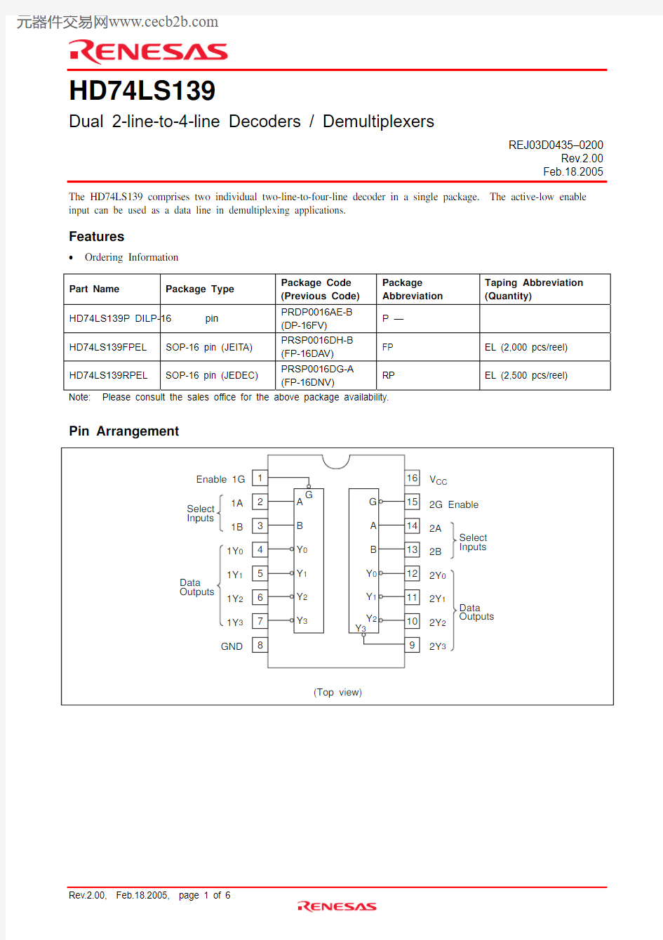
Feb.18.2005 The HD74LS139 comprises two individual two-line-to-four-line decoder in a single package. The active-low enable input can be used as a data line in demultiplexing applications.
Features
? Ordering Information
Part Name Package Type Package Code
(Previous Code)
Package
Abbreviation
Taping Abbreviation
(Quantity)
HD74LS139P DILP-16
pin PRDP0016AE-B
(DP-16FV)
P —
HD74LS139FPEL SOP-16 pin (JEITA) PRSP0016DH-B
(FP-16DAV)
FP EL (2,000 pcs/reel)
HD74LS139RPEL SOP-16 pin (JEDEC) PRSP0016DG-A
(FP-16DNV)
RP EL (2,500 pcs/reel)
Note: Please consult the sales office for the above package availability. Pin Arrangement
Function Table
Inputs
Outputs
Enable Select
G B A Y0Y1Y2Y3
H X X H H H H
L L L L H H H
L L H H L H H
L H L H H L H
L H H H H H L
H ; high level, L ; low level, X ; irrelevant
Block Diagram
Absolute Maximum Ratings
Unit
Ratings
Item Symbol
Supply voltage V CC 7 V Input voltage V IN 7 V Power dissipation P T 400 mW Storage temperature Tstg –65 to +150 °C
Note: Voltage value, unless otherwise noted, are with respect to network ground terminal.
Recommended Operating Conditions
Max
Typ
Unit Item Symbol
Min
Supply voltage V CC 4.75 5.00 5.25 V
I OH — — –400 μA
Output current
I OL — — 8 mA
°C
75
25
–20
Operating temperature Topr
Electrical Characteristics
(Ta = –20 to +75 °C)
Item
Symbol min. typ.* max. Unit Condition V IH 2.0 — — V Input voltage
V IL — — 0.8 V V OH 2.7 — — V V CC = 4.75 V, V IH = 2 V, V IL = 0.8 V,
I OH = –400 μA
— — 0.4 I OL = 4 mA Output voltage
V OL — — 0.5 V
I OL = 8 mA V CC = 4.75 V, V IH = 2 V,
V IL = 0.8 V
I IH — — 20 μA V CC = 5.25 V, V I = 2.7 V I IL — — –0.4 mA V CC = 5.25 V, V I = 0.4 V
Input current
I I —
— 0.1 mA V CC = 5.25 V, V I = 7 V Short-circuit output
current
I OS –5
— –42 mA V CC = 5.25 V Supply current I CC — 6.8 11 mA V CC = 5.25 V, Outputs enabled and open Input clamp voltage V IK — — –1.5 V V CC = 4.75 V, I IN = –18 mA Note: * V CC = 5 V, Ta = 25°C
Switching Characteristics
(V CC = 5 V, Ta = 25°C)
Item Symbol Inputs Output Levels
of delay
min. typ. max. Unit Condition
t PLH — 13 20 ns t PHL 2 — 22 33 ns t PLH — 18 29 ns t PLH
Binary select 1A, 1B 2A, 2B 1Y 0 to 1Y 3
2Y 0 to 2Y 3 3
— 25 38 ns t PLH — 16 24 ns Propagation
delay time t PHL
Enable 1G, 2G 1Y 0 to 1Y 3
2Y 0 to 2Y 3 2
— 21 32 ns C L = 15 pF,R L = 2 k ?
Testing Method Test Circuit
Waveform
Package Dimensions
https://www.360docs.net/doc/b74339413.html, RENESAS SALES OFFICES
Refer to "https://www.360docs.net/doc/b74339413.html,/en/network" for the latest and detailed information.
Renesas Technology America, Inc.
450 Holger Way, San Jose, CA 95134-1368, U.S.A
Tel: <1> (408) 382-7500, Fax: <1> (408) 382-7501
Renesas Technology Europe Limited
Dukes Meadow, Millboard Road, Bourne End, Buckinghamshire, SL8 5FH, U.K.
Tel: <44> (1628) 585-100, Fax: <44> (1628) 585-900
Renesas Technology Hong Kong Ltd.
7th Floor, North Tower, World Finance Centre, Harbour City, 1 Canton Road, Tsimshatsui, Kowloon, Hong Kong
Tel: <852> 2265-6688, Fax: <852> 2730-6071
Renesas Technology Taiwan Co., Ltd.
10th Floor, No.99, Fushing North Road, Taipei, Taiwan
Tel: <886> (2) 2715-2888, Fax: <886> (2) 2713-2999
Renesas Technology (Shanghai) Co., Ltd.
Unit2607 Ruijing Building, No.205 Maoming Road (S), Shanghai 200020, China
Tel: <86> (21) 6472-1001, Fax: <86> (21) 6415-2952
Renesas Technology Singapore Pte. Ltd.
1 Harbour Front Avenue, #06-10, Keppel Bay Tower, Singapore 098632
Tel: <65> 6213-0200, Fax: <65> 6278-8001