MRF6S27015GNR1;MRF6S27015NR1;中文规格书,Datasheet资料
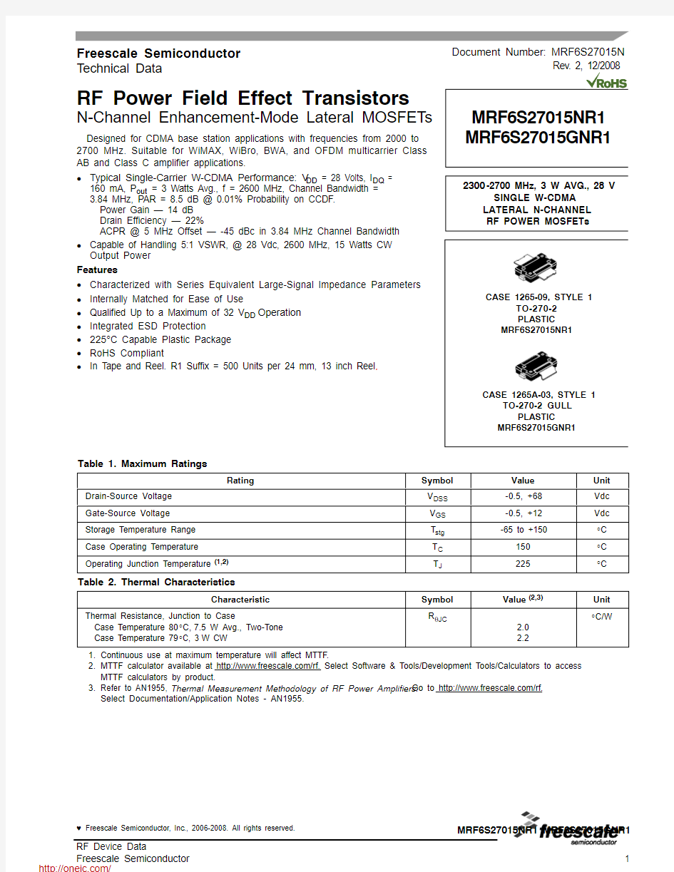
RF Power Field Effect Transistors
N-Channel Enhancement-Mode Lateral MOSFETs
Designed for CDMA base station applications with frequencies from 2000 to
2700 MHz. Suitable for WiMAX, WiBro, BWA, and OFDM multicarrier Class
AB and Class C amplifier applications.
?Typical Single-Carrier W-CDMA Performance: V DD = 28 Volts, I DQ =
160 mA, P out = 3 Watts Avg., f = 2600 MHz, Channel Bandwidth =
3.84 MHz, PAR = 8.5 dB @ 0.01% Probability on CCDF.
Power Gain — 14 dB
Drain Efficiency — 22%
ACPR @ 5 MHz Offset — -45 dBc in 3.84 MHz Channel Bandwidth
?Capable of Handling 5:1 VSWR, @ 28 Vdc, 2600 MHz, 15 Watts CW
Output Power
Features
?Characterized with Series Equivalent Large-Signal Impedance Parameters
?Internally Matched for Ease of Use
?Qualified Up to a Maximum of 32 V DD Operation
?Integrated ESD Protection
?225°C Capable Plastic Package
?RoHS Compliant
?In Tape and Reel. R1 Suffix = 500 Units per 24 mm, 13 inch Reel.
Table 1. Maximum Ratings
Rating Symbol Value Unit Drain-Source Voltage V DSS-0.5, +68Vdc Gate-Source Voltage V GS-0.5, +12Vdc Storage Temperature Range T stg-65 to +150°C Case Operating Temperature T C150°C Operating Junction Temperature(1,2)T J225°C Table 2. Thermal Characteristics
Characteristic Symbol Value (2,3)Unit Thermal Resistance, Junction to Case
Case Temperature 80°C,7.5 W Avg., Two-Tone
Case Temperature 79°C, 3W CW
RθJC
2.0
2.2
°C/W
1.Continuous use at maximum temperature will affect MTTF.
2.MTTF calculator available at https://www.360docs.net/doc/b06123739.html,/rf. Select Software & Tools/Development Tools/Calculators to access
MTTF calculators by product.
3.Refer to AN1955, Thermal Measurement Methodology of RF Power Amplifiers. Go to https://www.360docs.net/doc/b06123739.html,/rf.
Select Documentation/Application Notes - AN1955.
Document Number: MRF6S27015N
Rev. 2, 12/2008 Freescale Semiconductor
Technical Data
2
RF Device Data
Freescale Semiconductor
MRF6S27015NR1 MRF6S27015GNR1Table 3. ESD Protection Characteristics
Test Methodology
Class Human Body Model (per JESD22-A114)1A (Minimum)Machine Model (per EIA/JESD22-A115) A (Minimum)Charge Device Model (per JESD22-C101)
IV (Minimum)
Table 4. Moisture Sensitivity Level
Test Methodology
Rating Package Peak Temperature
Unit Per JESD 22-A113, IPC/JEDEC J-STD-020
3
260
°C
Table 5. Electrical Characteristics (T C = 25°C unless otherwise noted)
Characteristic
Symbol
Min
Typ
Max
Unit
Off Characteristics
Zero Gate Voltage Drain Leakage Current (V DS = 68 Vdc, V GS = 0 Vdc)I DSS ——10μAdc Zero Gate Voltage Drain Leakage Current (V DS = 28 Vdc, V GS = 0 Vdc)I DSS ——1μAdc Gate-Source Leakage Current (V GS = 5 Vdc, V DS = 0 Vdc)I GSS
—
—
500
nAdc
On Characteristics
Gate Threshold Voltage
(V DS = 10 Vdc, I D = 40 μAdc)V GS(th) 1.5 2.2 3.5Vdc Gate Quiescent Voltage
(V DS = 28 Vdc, I D = 160 mAdc)
V GS(Q)— 2.8—Vdc Fixture Gate Quiescent Voltage (1)
(V DD = 28 Vdc, I D = 160 mAdc, Measured in Functional Test)V GG(Q) 2.2 3.1 4.4Vdc Drain-Source On-Voltage
(V GS = 10 Vdc, I D = 0.4 Adc)V DS(on)
—
0.27
0.4
Vdc
Dynamic Characteristics (2)
Reverse Transfer Capacitance
(V DS = 28 Vdc ± 30 mV(rms)ac @ 1 MHz, V GS = 0 Vdc)C rss —11.6—pF Output Capacitance
(V DS = 28 Vdc ± 30 mV(rms)ac @ 1 MHz, V GS = 0 Vdc)
C oss
—
22.9
—
pF
Functional Tests (3) (In Freescale Test Fixture, 50 ohm system) V DD = 28 Vdc, I DQ = 160 mA, P out = 3 W Avg., f = 2600 MHz, Single-Carrier W-CDMA, 3.84 MHz Channel Bandwidth Carriers. ACPR measured in 3.84 MHz Channel Bandwidth @ ±5 MHz Offset. PAR = 8.5 dB @0.01% Probability on CCDF. Power Gain G ps 12.51416dB Drain Efficiency
ηD 1922—%Adjacent Channel Power Ratio ACPR —-45-42dBc Input Return Loss
IRL
—
-18
-9
dB
1.V GG = 11/10 x V GS(Q). Parameter measured on Freescale Test Fixture, due to resistive divider network on the board. Refer to T est Circuit schematic.
2.Part internally input matched.
3.Measurement made with device in straight lead configuration before any lead forming operation is applied.
https://www.360docs.net/doc/b06123739.html,/
MRF6S27015NR1 MRF6S27015GNR1
3
RF Device Data
Freescale Semiconductor
Figure 1. MRF6S27015NR1(GNR1) Test Circuit Schematic
Z110.143″ x 0.816″ Microstrip Z120.101″ x 0.667″ Microstrip Z130.073″ x 0.485″ Microstrip Z140.120″ x 0.021″ Microstrip Z150.407″ x 0.170″ Microstrip Z160.714″ x 0.066″ Microstrip Z170.496″ x 0.066″ Microstrip Z180.475″ x 0.050″ Microstrip Z190.480″ x 0.050″ Microstrip
PCB
Taconic RF-35, 0.030″, εr = 3.5
Z10.503″ x 0.066″ Microstrip Z20.905″ x 0.066″ Microstrip
Z30.371″ x 0.300″ x 0.049″ Taper Z40.041″ x 0.016″ Microstrip Z50.245″ x 0.851″ Microstrip Z60.248″ x 0.851″ Microstrip Z70.973″ x 0.050″ Microstrip Z80.085″ x 0.485″ Microstrip Z90.091″ x 0.667″ Microstrip Z100.138″ x 0.816″ Microstrip
Table 6. MRF6S27015NR1(GNR1) Test Circuit Component Designations and Values
Part
Description
Part Number
Manufacturer C1100 nF Chip Capacitor CDR33BX104AKYS Kemet C2 4.7 pF Chip Capacitor ATC100B4R7BT500XT ATC C39.1 pF Chip Capacitor ATC100B9R1BT500XT ATC C4, C5, C68.2 pF Chip Capacitors ATC100B8R2BT500XT ATC C7, C8, C9, C1010 μF, 50 V Chip Capacitors GRM55DR61H106KA88L Murata C1110 μF, 35 V Tantalum Chip Capacitor T491D106K035AT Kemet R1 1 K Ω, 1/4 W Chip Resistor CRCW12061001FKEA Vishay R210 K Ω,1/4 W Chip Resistor CRCW12061002FKEA Vishay R3
10 Ω, 1/4 W Chip Resistor
CRCW120610R0FKEA
Vishay
https://www.360docs.net/doc/b06123739.html,/
4
RF Device Data
Freescale Semiconductor
MRF6S27015NR1 MRF6S27015GNR1Figure 2. MRF6S27015NR1(GNR1) Test Circuit Component Layout
https://www.360docs.net/doc/b06123739.html,/
MRF6S27015NR1 MRF6S27015GNR1
5
RF Device Data
Freescale Semiconductor
TYPICAL CHARACTERISTICS
Figure 5. Two-Tone Power Gain versus
Output Power 12
16
1
P out , OUTPUT POWER (WATTS) PEP
14
1310
G p s , P O W E R G A I N (d B )
Figure 6. Third Order Intermodulation Distortion
versus Output Power
1P out , OUTPUT POWER (WATTS) PEP
10
15
https://www.360docs.net/doc/b06123739.html,/
6
RF Device Data
Freescale Semiconductor
MRF6S27015NR1 MRF6S27015GNR1TYPICAL CHARACTERISTICS
I M D , I N T E R M O D U L A T I O N D I S T O R T I O N (d B c )
?65
?15?40?50?30?20?60Figure 10. Single-Carrier W-CDMA ACPR, ALT1, Power
Gain and Drain Efficiency versus Output Power
P out , OUTPUT POWER (WATTS) AVG.
10
ηD ,1
?55?45?35?25https://www.360docs.net/doc/b06123739.html,/
MRF6S27015NR1 MRF6S27015GNR1
7
RF Device Data
Freescale Semiconductor
TYPICAL CHARACTERISTICS
10181
P out , OUTPUT POWER (WATTS) CW Figure 11. Power Gain and Drain Efficiency
versus CW Output Power
10
1716
15141312G p s , P O W E R G A I N (d B )
11Figure 12. Power Gain versus Output Power
P out , OUTPUT POWER (WATTS) CW
30
5
15
20
25
10
E V M , E R R O R V E C T O R M A G N I T U D E (%)
Figure 13. Drain Efficiency and Error Vector
Magnitude versus Output Power
0.5
P out , OUTPUT POWER (dBm)
25
31510
2.55
2
213536
1.5
ηD , D R A I N E F F I C I E N C Y (%)
20122232526272824343329303231250
109
90
T J , JUNCTION TEMPERATURE (°C)
Figure 14. MTTF versus Junction Temperature
This above graph displays calculated MTTF in hours when the device is operated at V DD = 28 Vdc, P out = 3 W Avg., and ηD = 22%.MTTF calculator available at https://www.360docs.net/doc/b06123739.html,/rf. Select Software & Tools/Development Tools/Calculators to access MTTF calculators by product.
108
107
106
110
130
150
170
190
M T T F (H O U R S )
210
230
https://www.360docs.net/doc/b06123739.html,/
8
RF Device Data
Freescale Semiconductor
MRF6S27015NR1 MRF6S27015GNR1W-CDMA TEST SIGNAL
?60?110
?10(d B )
?20?30?40?50?70?80?90?100
7.2
1.8
5.4
3.6
?1.8
?3.6?5.4?9
9
f, FREQUENCY (MHz)
Figure 15. CCDF W-CDMA 3GPP , Test Model 1, 64 DPCH, 67% Clipping, Single-Carrier Test Signal
?7.210
0.0001
1000
PEAK?TO?AVERAGE (dB)
10
10.10.010.0012
4
6
8
P R O B A B I L I T Y (%)
Figure 16. Single-Carrier W-CDMA Spectrum
https://www.360docs.net/doc/b06123739.html,/
MRF6S27015NR1 MRF6S27015GNR1
9
RF Device Data
Freescale Semiconductor
Z o = 5 Ω
Z load
f = 2500 MHz
Z source
f = 2700 MHz
f = 2500 MHz
f = 2700 MHz
V DD = 28 Vdc, I DQ = 160 mA, P out = 3 W Avg.f MHz Z
source
W Z load W 2500 4.059 - j2.284 3.380 - j0.543
2525 3.679 - j2.593 3.265 - j0.5462550 3.006 - j2.574 3.077 - j0.4492575 2.355 - j2.190 2.892 - j0.3362600 2.075 - j1.657 2.727 - j0.1822625 1.930 - j1.179 2.564 - j0.0342650 1.973 - j0.771 2.435 + j0.1402675 2.017 - j0.557 2.286 + j0.3402700
2.024 - j0.379
2.227 + j0.538
Z source =Test circuit impedance as measured from
gate to ground.Z load
=Test circuit impedance as measured
from drain to ground.
Z
source
Z
load
Output Matching Network
Figure 17. Series Equivalent Source and Load Impedance
https://www.360docs.net/doc/b06123739.html,/
10
RF Device Data
Freescale Semiconductor
MRF6S27015NR1 MRF6S27015GNR1Table 7. Common Source Scattering Parameters (V DD = 28 V, I DQ = 160 mA, T C = 25°C, 50 ohm system)
f MH S 11
S 21
S 12
S 22
MHz |S 11|∠φ|S 21|∠φ|S 12|∠φ|S 22|∠φ5000.984-178.2 1.45339.20.001-109.80.870-122.35500.984-179.0 1.18036.50.000-121.00.888-127.66000.986180.00.95834.40.000159.60.901-132.06500.987179.00.77633.00.001118.40.911-135.87000.987178.10.62732.30.001106.50.921-139.17500.986177.30.50232.50.001104.20.931-142.18000.985176.50.39734.10.00296.00.940-144.88500.985175.80.30837.70.00295.60.944-147.39000.984175.10.23544.50.00394.00.951-149.59500.983174.50.18056.50.00391.20.956-151.510000.982173.80.14675.60.00391.20.962-153.410500.981173.20.14298.90.00489.90.965-155.211000.980172.50.163118.00.00489.20.969-156.811500.978171.90.199129.90.00588.90.973-158.312000.976171.20.243136.60.00587.40.976-159.812500.974170.50.291140.20.00686.50.980-161.113000.970169.80.342141.80.00686.30.983-162.413500.966169.00.395142.10.00684.60.986-163.714000.960168.30.452141.50.00684.80.988-164.914500.953167.50.514140.20.00786.90.990-166.115000.945166.60.580138.40.00792.50.993-167.315500.933165.80.655135.90.009100.30.992-168.416000.918164.90.738132.50.01193.70.994-169.416500.901164.10.828128.40.01383.60.996-170.417000.879163.20.925123.50.01475.40.997-171.617500.850162.5 1.030117.60.01469.10.998-172.818000.815162.2 1.139110.80.01562.80.995-173.918500.775162.5 1.246102.70.01655.80.991-175.019000.734164.0 1.33793.60.01648.20.984-176.019500.700167.0 1.39983.50.01540.30.976-176.920000.683171.0 1.42073.10.01533.20.966-177.620500.687175.1 1.39662.90.01426.50.957-178.021000.710178.5 1.33853.40.01222.10.951-178.321500.741-179.3 1.25945.00.01119.80.948-178.622000.774-178.2 1.16937.60.01019.70.947-178.922500.805-177.8 1.07931.10.00919.70.947-179.223000.832-177.90.99325.80.00819.60.948-179.52350
0.855
-178.2
0.917
21.2
0.007
22.6
0.950
-179.9(continued)
https://www.360docs.net/doc/b06123739.html,/
分销商库存信息:
FREESCALE
MRF6S27015GNR1MRF6S27015NR1