TN2535中文资料
11/12/01
Supertex Inc. does not recommend the use of its products in life support applications and will not knowingly sell its products for use in such applications unless it receives an adequate "products liability
TN2535
N-Channel Enhancement-Mode Vertical DMOS FETs
Features
?Low threshold ?High input impedance
?Low input capacitance — 125pF max.?Fast switching speeds ?Low on resistance
?Free from secondary breakdown ?Low input and output leakage
Applications
?Logic level interfaces – ideal for TTL and CMOS ?Solid state relays ?Battery operated systems ?Photo voltaic drives ?Analog switches
?General purpose line drivers ?Telecom switches
Low Threshold DMOS Technology
These low threshold enhancement-mode (normally-off) transis-tors utilize a vertical DMOS structure and Supertex's well-proven silicon-gate manufacturing process. This combination produces devices with the power handling capabilities of bipolar transistors and with the high input impedance and positive temperature coefficient inherent in MOS devices. Characteristic of all MOS structures, these devices are free from thermal runaway and thermally induced secondary breakdown.
Supertex’s vertical DMOS FETs are ideally suited to a wide range of switching and amplifying applications where very low threshold voltage, high breakdown voltage, high input impedance, low input capacitance, and fast switching speeds are desired.
Absolute Maximum Ratings
Drain-to-Source Voltage BV DSS Drain-to-Gate Voltage BV DGS Gate-to-Source Voltage
± 20V
Operating and Storage Temperature -55°C to +150°C
Soldering Temperature*
300°C
* Distance of 1.6 mm from case for 10 seconds.
Ordering Information
BV DSS /R DS(ON)V GS(th)I D(ON)BV DGS (max)(max)(min)TO-243AA*350V
10?
2.0V
1.0A
TN2535N8
* Same as SOT-89. Product supplied on 2000 piece carrier tape reels.
Order Number / Package
New Product
Low Threshold
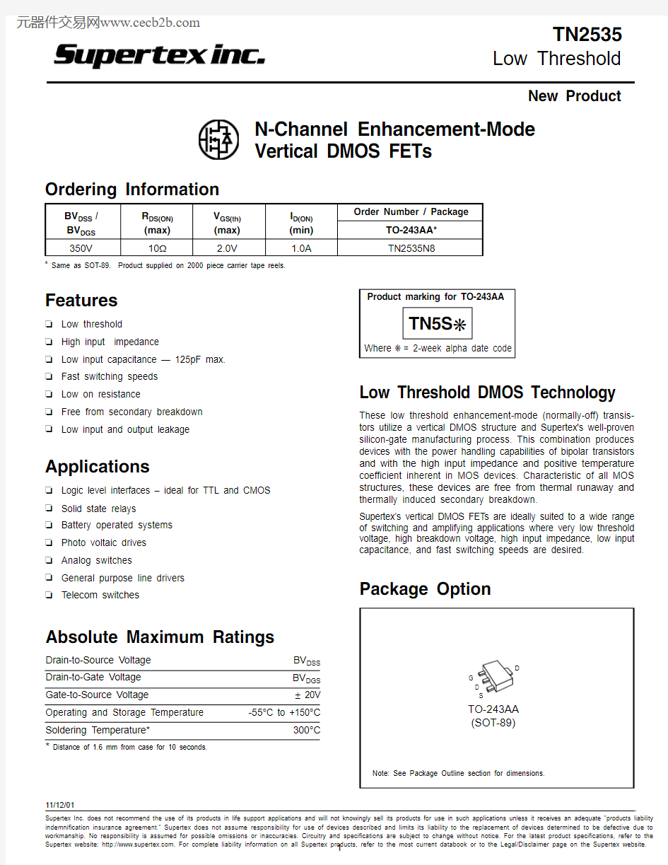
Package Option
Product marking for TO-243AA
Where ? = 2-week alpha date code
TN5S ?
元器件交易网https://www.360docs.net/doc/b29221292.html,
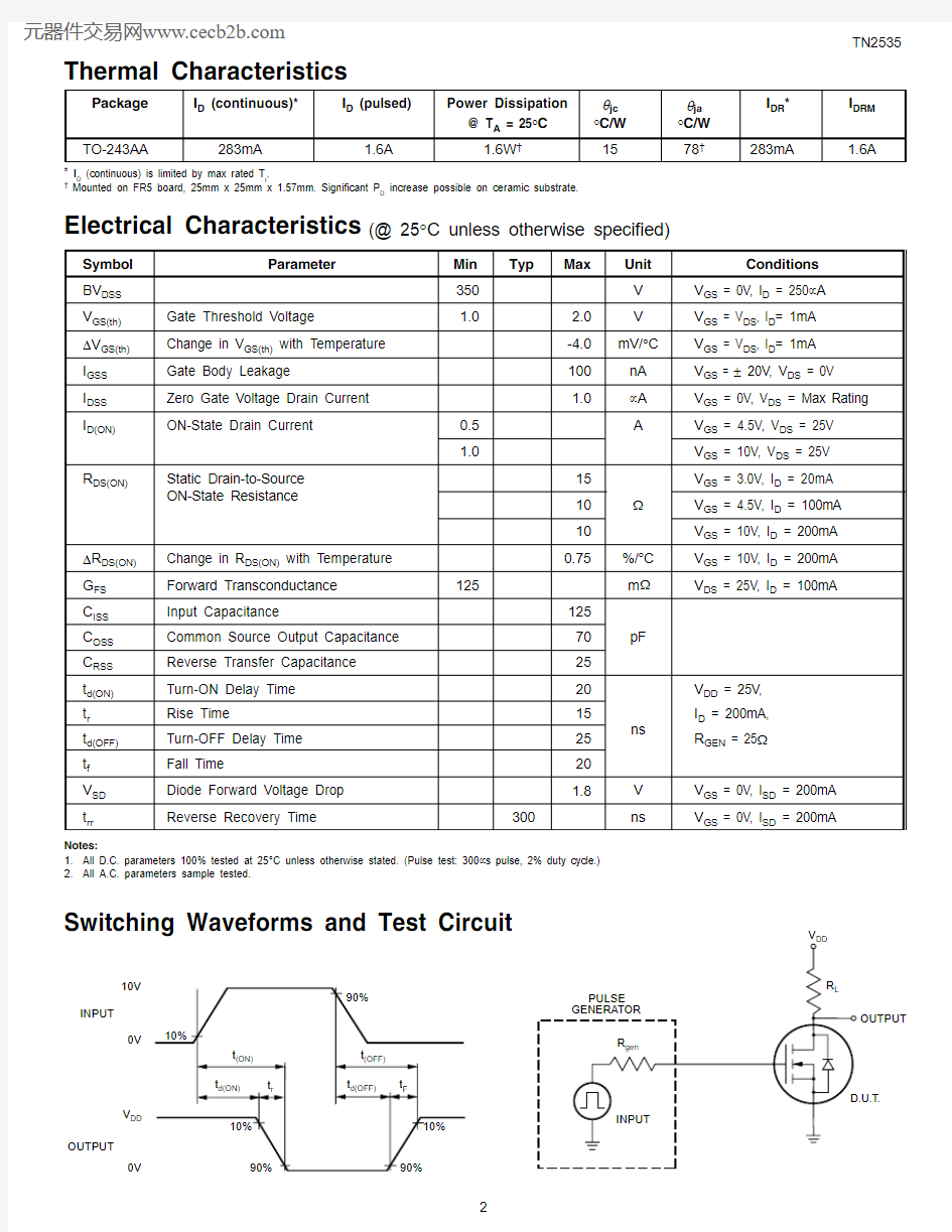
OUTPUT
INPUT
OUTPUT
10V
V DD
0V
0V
Thermal Characteristics
Switching Waveforms and Test Circuit
Package I D (continuous)*
I D (pulsed)
Power Dissipation θjc θja I DR *I DRM @ T A = 25°C
°C/W °C/W TO-243AA
283mA
1.6A
1.6W ?
15
78?
283mA
1.6A
* I D (continuous) is limited by max rated T j .?
Mounted on FR5 board, 25mm x 25mm x 1.57mm. Significant P D increase possible on ceramic substrate.
Symbol Parameter
Min Typ
Max
Unit Conditions
BV DSS 350V V GS = 0V, I D = 250μA V GS(th)Gate Threshold Voltage
1.0
2.0V V GS = V DS , I D = 1mA ?V GS(th)Change in V GS(th) with Temperature -4.0mV/°C V GS = V DS , I D = 1mA I GSS Gate Body Leakage
100nA V GS = ± 20V, V DS = 0V I DSS Zero Gate Voltage Drain Current 1.0
μA V GS = 0V, V DS = Max Rating I D(ON)
ON-State Drain Current
0.5A
V GS = 4.5V, V DS = 25V 1.0
V GS = 10V, V DS = 25V R DS(ON)
Static Drain-to-Source 15V GS = 3.0V, I D = 20mA ON-State Resistance
10?
V GS = 4.5V, I D = 100mA 10
V GS = 10V, I D = 200mA ?R DS(ON)Change in R DS(ON) with Temperature 0.75
%/°C V GS = 10V, I D = 200mA G FS Forward Transconductance 125
m V DS = 25V, I D = 100mA
C ISS Input Capacitance
125C OSS Common Source Output Capacitance 70pF
C RSS Reverse Transfer Capacitance 25t d(ON)Turn-ON Delay Time 20V D
D = 25V,t r Rise Time
15ns
I D = 200mA,t d(OFF)Turn-OFF Delay Time 25R GEN = 25?
t f Fall Time
20V SD Diode Forward Voltage Drop 1.8
V V GS = 0V, I SD = 200mA t rr
Reverse Recovery Time
300
ns
V GS = 0V, I SD = 200mA
Notes:
1.All D.C. parameters 100% tested at 25°C unless otherwise stated. (Pulse test: 300μs pulse, 2% duty cycle.)
2.All A.C. parameters sample tested.
Electrical Characteristics (@ 25°C unless otherwise specified)
?
I D (A m p e r e s )
V DS (Volts)
Output Characteristics
Saturation Characteristics
I D (A m p e r e s )
V DS (Volts)
G F S (S i e m e n s )
I D (Amperes)
Transconductance vs.Drain Current
Power Dissipation vs.Ambient Temperature
P D (W a t t s )
T A (?C)
Maximum Rated Safe Operating Area
I D (A m p e r e s )
V DS (Volts)Thermal Response Characteristics
T h e r m a l R e s i s t a n c e (n o r m a l i z e d )
t p (seconds)
1
1000
100
10
0.01
0.1
1.0
10
1.0
0.8
0.6
0.4
0.2
0.001
10
0.010.11
0.00.4
0.8
1.2
1.6
2.0
0.0
0.20.4
0.6
0.8
1.0
1.2
0.0
0.4
0.8
1.2
1.6
2.0
1235 Bordeaux Drive, Sunnyvale, CA 94089TEL: (408) 744-0100 ? FAX: (408) 222-4895
11/12/01
R D S (O N )(o h m s )
I D (Amperes)
On Resistance vs.Drain Current
V GS(th)and R DS(ON)w/Temperature
V G S (t h )(n o r m a l i z e d )
T J (?C)
R D S (O N )(n o r m a l i z e d )
Transfer Characteristics
I D (A m p e r e s )
V GS (Volts)
0.80.9
1.0
1.1
1.2
B V D S S (n o r m a l i z e d )
T J (?C)
BV DSS Variation with Temperature
Capacitance vs.Drain Source Voltage
C (p i c o f a r a d s )
V DS (Volts)
0.70.8
0.91.01.1
1.2
0.40.8
1.2
1.6
2.0
2.4
50
100
150
200
Gate Drive Dynamic Characteristics
Q (nanocoulombs)
G V G S (v o l t s )