STP140NF75中文资料
1/14
AUTOMOTIVE SPECIFIC
December 2002STB140NF75 STP140NF75
STB140NF75-1
N-CHANNEL 75V - 0.0065 ? -120A D2PAK/I2PAK/TO-220
STripFET? II POWER MOSFET
s TYPICAL R DS (on) = 0.0065 ?
s
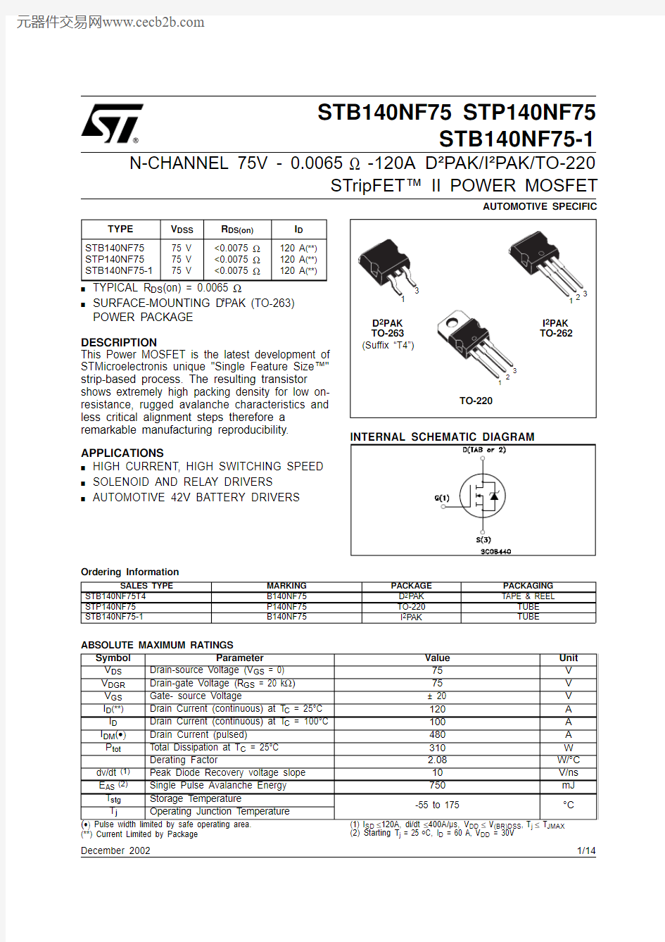
SURFACE-MOUNTING D 2PAK (TO-263) POWER PACKAGE
DESCRIPTION
This Power MOSFET is the latest development of STMicroelectronis unique "Single Feature Size?"strip-based process. The resulting transistor shows extremely high packing density for low on-resistance, rugged avalanche characteristics and less critical alignment steps therefore a remarkable manufacturing reproducibility.APPLICATIONS
s HIGH CURRENT, HIGH SWITCHING SPEED s SOLENOID AND RELAY DRIVERS
s AUTOMOTIVE 42V BATTERY DRIVERS
TYPE V DSS R DS(on)I D STB140NF75STP140NF75STB140NF75-1
75 V 75 V 75 V
<0.0075 ?<0.0075 ?<0.0075 ?
120 A (**)120 A (**)120 A (**)
Ordering Information
ABSOLUTE MAXIMUM RATINGS
Pulse width limited by safe operating area.
(**) Current Limited by Package
(1) I SD ≤120A, di/dt ≤400A/μs, V DD ≤ V (BR)DSS , T j ≤ T JMAX (2) Starting T j = 25 o C, I D = 60 A, V DD = 30V
SALES TYPE
MARKING PACKAGE PACKAGING STB140NF75T4B140NF75D 2PAK TAPE & REEL
STP140NF75P140NF75TO-220TUBE STB140NF75-1
B140NF75
I 2PAK
TUBE
Symbol Parameter Value Unit V DS Drain-source Voltage (V GS = 0)
75V V DGR
Drain-gate Voltage (R GS = 20 k ?)75V V GS Gate- source Voltage
± 20V I D (**)
Drain Current (continuous) at T C = 25°C 120A I D
Drain Current (continuous) at T C = 100°C 100A I DM (?)Drain Current (pulsed)480A P tot Total Dissipation at T C = 25°C
310W Derating Factor
2.08W/°C dv/dt (1)Peak Diode Recovery voltage slope 10V/ns E AS (2)Single Pulse Avalanche Energy 750mJ T stg Storage Temperature -55 to 175
°C
T j Operating Junction Temperature
STB140NF75 STP140NF75 STB150NF75-1
2/14
THERMAL DATA
ELECTRICAL CHARACTERISTICS (T case = 25 °C unless otherwise specified)OFF
ON (*)
DYNAMIC
Rthj-case Thermal Resistance Junction-case Max 0.48°C/W Rthj-amb Thermal Resistance Junction-ambient Max 62.5
°C/W Rthj-pcb Thermal Resistance Junction-pcb
Max
see curve on page 6
°C/W T l
Maximum Lead Temperature For Soldering Purpose (for 10 sec. 1.6 mm from case)
300
°C
Symbol Parameter
Test Conditions
Min.Typ.
Max.
Unit V (BR)DSS Drain-source
Breakdown Voltage I D = 250 μA
V GS = 0
75
V I DSS
Zero Gate Voltage
Drain Current (V GS = 0)V DS = Max Rating
V DS = Max Rating T C = 125°C 110μA μA I GSS
Gate-body Leakage Current (V DS = 0)
V GS = ± 20 V
±100
nA
Symbol Parameter
Test Conditions
Min.Typ.
Max.Unit V GS(th)Gate Threshold Voltage V DS = V GS I D = 250 μA 2
4V R DS(on)
Static Drain-source On Resistance
V GS = 10 V
I D = 70 A
0.00650.0075
?
Symbol Parameter
Test Conditions
Min.
Typ.Max.
Unit g fs (*)Forward Transconductance V DS = 15 V
I D =70 A
160S C iss C oss C rss
Input Capacitance Output Capacitance Reverse Transfer Capacitance
V DS = 25V, f = 1 MHz, V GS = 0
5000960310
pF pF pF
3/14
STB140NF75 STP140NF75 STB150NF75-1
SWITCHING ON
SWITCHING OFF
SOURCE DRAIN DIODE
Pulsed: Pulse duration = 300 μs, duty cycle 1.5 %.(?)Pulse width limited by safe operating area.
Symbol Parameter
Test Conditions
Min.Typ.Max.Unit t d(on)t r Turn-on Delay Time Rise Time
V DD = 38 V
I D = 70 A R G =4.7 ? V GS = 10 V (Resistive Load, Figure 3)30140ns ns
Q g Q gs Q gd
Total Gate Charge Gate-Source Charge Gate-Drain Charge
V DD =60 V I D =120A V
GS = 10V
(see test circuit, Figure 4)
1602870
218
nC nC nC
Symbol Parameter
Test Conditions
Min.
Typ.Max.
Unit t d(off)t f
Turn-off Delay Time Fall Time
V DD = 38 V
I D = 70 A R G =4.7?, V GS = 10 V (Resistive Load, Figure 3)
13090
ns ns
Symbol Parameter
Test Conditions
Min.
Typ.
Max.Unit I SD I SDM (?)Source-drain Current
Source-drain Current (pulsed)120480A A V SD (*)Forward On Voltage I SD = 120 A
V GS = 0
1.5
V t rr Q rr I RRM
Reverse Recovery Time Reverse Recovery Charge Reverse Recovery Current
I SD = 120 A
di/dt = 100A/μs V DD = 35 V T j = 150°C (see test circuit, Figure 5)
1154508
ns nC A
ELECTRICAL CHARACTERISTICS (continued)
STB140NF75 STP140NF75 STB150NF75-1
STB140NF75 STP140NF75 STB150NF75-1
STB140NF75 STP140NF75 STB150NF75-1
6/14
Allowable Iav vs. Time in Avalanche
The previous curve gives the safe operating area for unclamped inductive loads, single pulse or repetitive,under the following conditions:P D(AVE) = 0.5 * (1.3 * BV DSS * I AV )E AS(AR) = P D(AVE) * t AV
Where:
I AV is the Allowable Current in Avalanche
P D(AVE) is the Average Power Dissipation in Avalanche (Single Pulse)t AV is the Time in Avalanche
To derate above 25 o C, at fixed I AV , the following equation must be applied:
I AV = 2 * (T jmax - T CASE )/ (1.3 * BV DSS * Z th )
Where:
Z th = K * R th is the value coming from Normalized Thermal Response at fixed pulse width equal to T AV .
STB140NF75 STP140NF75 STB150NF75-1
Parameter Node Value CTHERM17 - 6 1.49 * 10-3 CTHERM2 6 - 5 3.50 * 10-2 CTHERM3 5 - 4 5.94 * 10-2 CTHERM4 4 - 39.74 * 10-2 CTHERM5 3 - 28.86 * 10-2 CTHERM6 2 - 18.27 * 10-1
RTHERM17 - 60.0384 RTHERM2 6 - 50.0624 RTHERM3 5 - 40.072 RTHERM4 4 - 30.0912 RTHERM5 3 - 20.1008 RTHERM6 2 - 1
0.1152
SPICE THERMAL MODEL
7/14
STB140NF75 STP140NF75 STB150NF75-1
8/14
Fig. 3: Switching Times Test Circuits For Resistive Fig. 3.1: Switching Time Waveform
STB140NF75 STP140NF75 STB150NF75-1 Fig. 5: Diode Switching Test Circuit
9/14
STB140NF75 STP140NF75 STB150NF75-1
10/14
DIM.mm.
inch.
MIN.TYP. MAX.
MIN.TYP. TYP .
A 4.4 4.60.1730.181A1 2.49 2.690.0980.106
A20.030.230.0010.009B 0.70.930.0280.037B2 1.14 1.70.0450.067C 0.450.60.0180.024C2 1.21 1.360.0480.054D 8.95
9.35
0.352
0.368
D18
0.315
E 10
10.4
0.394
0.409
E18.5
0.334
G 4.88 5.280.1920.208L 1515.850.5910.624L2 1.27 1.40.0500.055L3 1.4 1.750.0550.069M 2.4
3.2
0.094
0.126
R 0.4
0.015
V2
0°8°
0°
8°
D 2PAK MECHANICAL DATA
STB140NF75 STP140NF75 STB150NF75-1
12/14
DIM.mm.
inch.
MIN.TYP. MAX.
MIN.TYP. TYP .
A 4.4 4.60.1730.181C 1.23 1.320.0480.051D 2.40 2.720.0940.107E 0.490.700.0190.027F 0.610.880.0240.034F1 1.14 1.700.0440.067F2 1.14 1.700.0440.067G 4.95 5.150.1940.203G1 2.40 2.700.0940.106H210
10.40
0.393
0.409
L216.400.645L328.90
1.137
L413140.5110.551L5 2.65 2.950.1040.116L615.2515.750.6000.620L7 6.20 6.600.2440.260L9 3.50 3.930.1370.154DIA
3.75
3.85
0.147
0.151
TO-220 MECHANICAL DATA
13/14
STB140NF75 STP140NF75 STB150NF75-1
DIM.
mm inch
MIN.MAX.MIN.MAX.A010.510.70.4130.421B015.715.90.6180.626D 1.5 1.60.0590.063D1 1.59 1.610.0620.063E 1.65 1.850.0650.073F 11.411.60.4490.456K0 4.8 5.00.1890.197P0 3.9 4.10.1530.161P111.912.10.4680.476P2 1.9 2.1
00750.082
R 50 1.574T 0.250.35.0.00980.0137W
23.7
24.30.933
0.956DIM.mm inch
MIN.
MAX.MIN.
MAX.A 330
12.992
B 1.50.059
C 12.813.20.5040.520
D 20.20.795G 24.426.40.960 1.039N 100
3.937
T
30.4
1.197BASE QTY BULK QTY 1000
1000REEL MECHANICAL DATA
* on sales type
TUBE SHIPMENT (no suffix)*
TAPE AND REEL SHIPMENT (suffix ”T4”)*
D 2PAK FOOTPRINT TAP
E MECHANICAL DATA
STB140NF75 STP140NF75 STB150NF75-1
Information furnished is believed to be accurate and reliable. However, STMicroelectronics assumes no responsibility for the consequences of use of such information nor for any infringement of patents or other rights of third parties which may result from its use. No license is granted by implication or otherwise under any patent or patent rights of STMicroelectronics. Specifications mentioned in this publication are subject to change without notice. This publication supersedes and replaces all information previously supplied. STMicroelectronics products are not authorized for use as critical components in life support devices or systems without express written approval of STMicroelectronics.
The ST logo is registered trademark of STMicroelectronics
? 2002 STMicroelectronics - All Rights Reserved
All other names are the property of their respective owners.
STMicroelectronics GROUP OF COMPANIES
Australia - Brazil - Canada - China - Finland - France - Germany - Hong Kong - India - Israel - Italy - Japan - Malaysia - Malta - Morocco - Singapore - Spain - Sweden - Switzerland - United Kingdom - United States.
https://www.360docs.net/doc/bd15387356.html,
14/14