自旋极化注入

letters to nature
Acknowledgements
We acknowledge the?nancial support of the European Commission(Esprit project SPIDER)as well as the Bundesministerium fuèr Bildung und Forschung(Verbundprojekt Elektronische Korrelationen und Magnetismus).We would also like to thank Th.Gruber, V.Hock,B.Koènig,D.Yakovlev,G.Muèller and G.E.W.Bauer for discussions and help. Correspondence and requests for materials should be addressed to L.W.M.
(e-mail:laurens.molenkamp@physik.uni-wuerzburg.de).
................................................................. Electrical spin injection
in a ferromagnetic semiconductor heterostructure
Y.Ohno*,D.K.Young2,B.Beschoten2,F.Matsukura*,H.Ohno*
&D.D.Awschalom2
*Laboratory for Electronic Intelligent Systems,Research Institute of Electrical Communication,Tohoku University,Katahira2-1-1,Aoba-ku,Sendai980-8577, Japan
2Center for Spintronics and Quantum Computation,Quantum Institute, University of California,Santa Barbara,California93106,USA .............................................................................................................................................. Conventional electronics is based on the manipulation of electro-nic charge.An intriguing alternative is the?eld of`spintronics', wherein the classical manipulation of electronic spin in semicon-ductor devices gives rise to the possibility of reading and writing non-volatile information through magnetism1,2.Moreover,the ability to preserve coherent spin states in conventional semiconductors3and quantum dots4may eventually enable quan-tum computing in the solid state5,6.Recent studies have shown that optically excited electron spins can retain their coherence over distances exceeding100micrometres(ref.7).But to inject spin-polarized carriers electrically remains a formidable challenge8,9.Here we report the fabrication of all-semiconductor, light-emitting spintronic devices using III±V heterostructures based on gallium arsenide.Electrical spin injection into a non-magnetic semiconductor is achieved(in zero magnetic?eld)using a p-type ferromagnetic semiconductor10as the spin polarizer.Spin polarization of the injected holes is determined directly from the polarization of the emitted electroluminescence following the recombination of the holes with the injected(unpolarized) electrons.
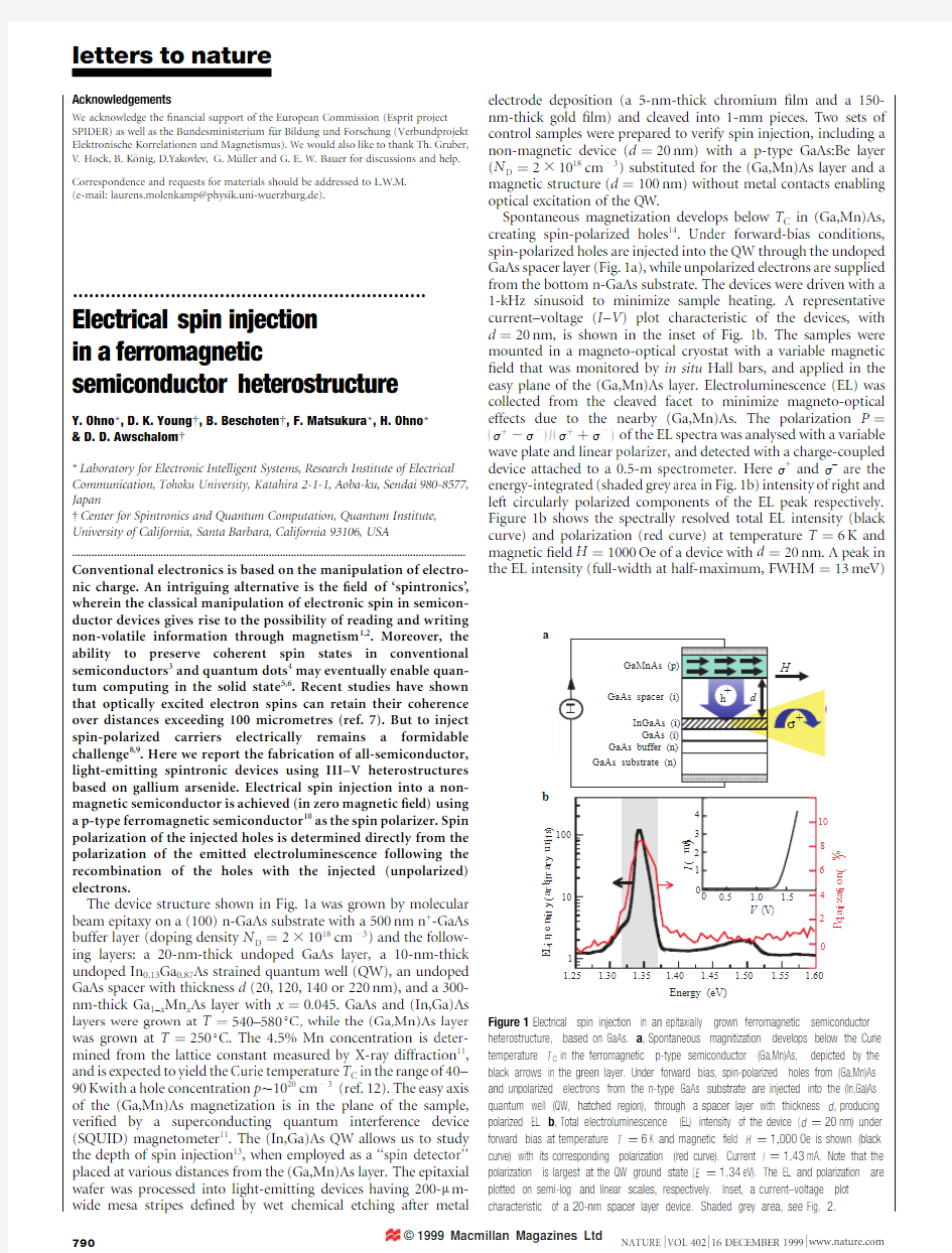
The device structure shown in Fig.1a was grown by molecular beam epitaxy on a(100)n-GaAs substrate with a500nm n+-GaAs buffer layer(doping density N D 231018cm23)and the follow-ing layers:a20-nm-thick undoped GaAs layer,a10-nm-thick undoped In0.13Ga0.87As strained quantum well(QW),an undoped GaAs spacer with thickness d(20,120,140or220nm),and a300-nm-thick Ga1-x Mn x As layer with x 0:045.GaAs and(In,Ga)As layers were grown at T 540±5808C,while the(Ga,Mn)As layer was grown at T 2508C.The4.5%Mn concentration is deter-mined from the lattice constant measured by X-ray diffraction11, and is expected to yield the Curie temperature T C in the range of40±90Kwith a hole concentration p,1020cm23(ref.12).The easy axis of the(Ga,Mn)As magnetization is in the plane of the sample, veri?ed by a superconducting quantum interference device (SQUID)magnetometer11.The(In,Ga)As QW allows us to study the depth of spin injection13,when employed as a``spin detector'' placed at various distances from the(Ga,Mn)As layer.The epitaxial wafer was processed into light-emitting devices having200-m m-wide mesa stripes de?ned by wet chemical etching after metal electrode deposition(a5-nm-thick chromium?lm and a150-nm-thick gold?lm)and cleaved into1-mm pieces.Two sets of control samples were prepared to verify spin injection,including a non-magnetic device(d 20nm)with a p-type GaAs:Be layer (N D 231018cm23)substituted for the(Ga,Mn)As layer and a magnetic structure(d 100nm)without metal contacts enabling optical excitation of the QW.
Spontaneous magnetization develops below T C in(Ga,Mn)As, creating spin-polarized holes14.Under forward-bias conditions, spin-polarized holes are injected into the QW through the undoped GaAs spacer layer(Fig.1a),while unpolarized electrons are supplied from the bottom n-GaAs substrate.The devices were driven with a 1-kHz sinusoid to minimize sample heating.A representative current±voltage(I±V)plot characteristic of the devices,with d 20nm,is shown in the inset of Fig.1b.The samples were mounted in a magneto-optical cryostat with a variable magnetic ?eld that was monitored by in situ Hall bars,and applied in the easy plane of the(Ga,Mn)As layer.Electroluminescence(EL)was collected from the cleaved facet to minimize magneto-optical effects due to the nearby(Ga,Mn)As.The polarization P j 2j2 = j j2 of the EL spectra was analysed with a variable wave plate and linear polarizer,and detected with a charge-coupled device attached to a0.5-m spectrometer.Here j+and j-are the energy-integrated(shaded grey area in Fig.1b)intensity of right and left circularly polarized components of the EL peak respectively. Figure1b shows the spectrally resolved total EL intensity(black curve)and polarization(red curve)at temperature T 6K and magnetic?eld H 1000Oe of a device with d 20nm.A peak in the EL intensity(full-width at half-maximum,FWHM 13meV)
a
E
L
i
n
t
e
n
s
i
t
y
(
a
r
b
i
t
r
a
r
y
u
n
i
t
s
)
P
o
l
a
r
i
z
a
t
i
o
n
(
%
)
Energy (eV)
b
Figure1Electrical spin injection in an epitaxially grown ferromagnetic semiconductor heterostructure,based on GaAs.a,Spontaneous magnitization develops below the Curie temperature T C in the ferromagnetic p-type semiconductor(Ga,Mn)As,depicted by the black arrows in the green layer.Under forward bias,spin-polarized holes from(Ga,Mn)As and unpolarized electrons from the n-type GaAs substrate are injected into the(In,Ga)As quantum well(QW,hatched region),through a spacer layer with thickness d,producing polarized EL.b,Total electroluminescence(EL)intensity of the device(d 20nm)under forward bias at temperature T 6K and magnetic?eld H 1;000Oe is shown(black curve)with its corresponding polarization(red curve).Current I 1:43mA.Note that the polarization is largest at the QW ground state(E 1:34eV).The EL and polarization are plotted on semi-log and linear scales,respectively.Inset,a current±voltage plot characteristic of a20-nm spacer layer device.Shaded grey area,see Fig.2.
letters to nature
and polarization is seen at the QW ground-state transition energy (E 1:34eV).The measured polarization contains a constant background due most likely to a combination of sample strain and experimental geometry.We note that the polarization ampli-tude is sensitive to the angle of collection,which may reˉect variation of the effective ?eld or directionality in the polarization induced by the waveguide of the structure.We also observe no systematic dependence of the polarization on either the spacer layer thickness or the injection current density.
Figure 2shows relative changes in EL polarization,D P [P 2P bkgd ,where P bkgd is the background polarization,as a function of in-plane magnetic ?eld for various temperatures above and below T C .Below T 31K,D P is hysteretic with loops closing at H <300Oe.The coercive ?eld increases from 0to 40Oe as the temperature decreases from T C to T 6K.The inset shows that the temperature dependence of the relative remanent polarization (D P at H 0Oe)at T 6±94K follows the sample's magnetic moment M (solid black curve),independently measured using a SQUID magnetometer.The deviation from Brillouin behaviour of M (T )is consistent with studies of the magnetization temperature depen-dence in (Ga,Mn)As 14,15.No polarization hysteresis is observed for T >52K,when (Ga,Mn)As becomes paramagnetic.
A non-magnetic device was grown in order to verify that the hysteresis in the polarization is due to spin injection rather than carrier polarization from the (Ga,Mn)As stray ?eld.In contrast to the magnetic devices,the EL polarization from this non-magnetic device (Fig.3a)shows no hysteresis at T 6K from 2500Oe ,H ,500Oe,thus linking the hysteretic polarization to the presence of a (Ga,Mn)As layer.Furthermore,the ?eld range over which we observe no change in the polarization is comparable to the stray ?eld expected at the (Ga,Mn)As facet (,500Oe)11.This suggests that local ?elds from the (Ga,Mn)As layer are unlikely to be responsible for the hysteretic polarization in the magnetic structures.
Since (Ga,Mn)As exhibits strong magnetic circular dichroism 14,it was also important to con?rm that the observed hysteretic polari-zation is not due to possible re-absorption of QW luminescence passing through the (Ga,Mn)As layer.A magnetic sample without metal contacts was prepared,allowing direct optical excitation of
unpolarized carriers into the QW.A p-type layer between the QW and a semi-insulating substrate was incorporated into the structure in order to reduce the electrostatic potential across the junction,thus leading to more ef?cient radiative recombination.Selective spectral excitation (FWHM ,1meV)by a continuous-wave Ti-sapphire laser was used to create unpolarized carriers in the QW by illuminating through the polished substrate (,80m m)with linearly polarized light at E 1:398eV,which is 53meV above the QW ground state.Light was collected from the cleaved facet with an identical optical path to the EL measurements.The photolumi-nescence (PL)polarization as a function of magnetic ?eld,shown in Fig.3b,shows no hysteresis,providing further evidence that spin injection is occurring in the magnetic samples.
The presence of hysteretic polarization observed in magnetic samples with d 20±220nm,and its absence in the control samples,indicate that hole spins can be injected and transported over 200nm.This occurs in spite of possible depolarization due to transport through interfaces,as well as valence band mixing in the bulk and QW regions.Additionally,hole spins can be preserved during energy relaxation in a QW 16.As opposed to the high energy injection of ``hot''carriers from metal/semiconductor junctions,energy relaxation from semiconductor p±n junctions that are in quasi-equilibrium is minimized,which may determine the length scale of spin transport in the present structure.It is still dif?cult to estimate the expected degree of EL polarization from these types of structures,as detailed knowledge about the relevant band structure and transport/optical properties of (Ga,Mn)As is not yet available.We have used epitaxially grown all-semiconductor ferromag-netic/non-magnetic structures to demonstrate electrical spin injec-tion and transport.Electroluminescence polarization reveals that the hole spin polarization in a ferromagnetic semiconductor can be transported across interfaces over distances greater than 200nm in a forward biased p±n junction structure,and switched in modest ?elds of H ,40Oe.The demonstration of electrical spin injection into a semiconductor,especially in the absence of an applied magnetic ?eld,suggests a variety of new technological opportu-nities,including electrical control of magnetization,integration of nonvolatile storage and logic,and manipulation of quantum spin states in semiconductors.M
Magnetic field (Oe)
R e l a t i v e c h a n g e i n p o l a r i z a t i o n (%)
Figure 2Hysteretic electroluminescence polarization is a direct result of spin injection from the ferromagnetic (Ga,Mn)As layer.Shown are relative changes in the energy-integrated (shaded grey area in Fig.1b)polarization D P ,at temperatures T 6±52K,as a function of in-plane ?eld from a device with d 140nm.E 1:34eV,I 2:8mA.Triangles indicate points taken when the ?eld is swept up or down.Inset,the relative remanent polarization (D P at H 0Oe)shown in solid squares at T 6±94K,and the temperature dependence of the (Ga,Mn)As magnetic moment,measured by a SQUID magnetometer (solid black curve),demonstrating that polarization is proportional to magnetic
moment.
100200300–300400–400–100
–200Magnetic field (Oe)
R e l a t i v e c h a n g e i n p o l a r i z a t i o n (%)
–500500
Figure 3The absence of hysteretic polarization.Data shown from a forward biased non-magnetic device at T 6K (a )and from a magnetic structure under optical excitation (b )verify that electrical spin injection occurs within the device depicted in Fig.1a.a ,Magnetic ?eld dependence of D P from a non-magnetic device is shown in contrast to a magnetic structure,with identical layers (d 20nm).Triangles as for Fig.2.b ,No hysteresis is observed from the photoluminescence (PL)polarization of a magnetic sample excited with E 1:398eV (QW PL ground state,E 1:345eV).
letters to nature
Received9September;accepted5November1999.
1.Awschalom,D.D.&Kikkawa,J.M.Electron spin and optical coherence in semiconductors.Phys.
Today52,33±38(1999).
2.Prinz,G.A.Magnetoelectronics.Science282,1660±1663(1998).
3.Kikkawa,J.M.&Awschalom,D.D.Resonant spin ampli?cation in n-type GaAs.Phys.Rev.Lett.80,
4313±4316(1998).
4.Gupta,J.A.,Awschalom,D.D.,Peng,X.&Alivisatos,A.P.Spin coherence in semiconductor quantum
dots.Phys.Rev.B59,10421±10424(1999).
5.DiVincenzo,D.P.Quantum computation.Science270,255±261(1995).
6.Loss,D.&DiVincenzo,D.P.Quantum computation with quantum dots.Phys.Rev.A57,120±126
(1998).
7.Kikkawa,J.M.&Awschalom,https://www.360docs.net/doc/c4141996.html,teral drag of spin coherence in gallium arsenide.Nature397,
139±141(1999).
8.Monzon,F.G.&Roukes,M.L.Spin injection and the local hall effect in InAs quantum wells.J.Mag.
Magn.Mater.198,632±635(1999).
9.Hammar,P.R.et al.Observation of the spin injection at a ferromagnetic-semiconductor interface.
Phys.Rev.Lett.83,203±206(1999).
10.Ohno,H.Making nonmagnetic semiconductors ferromagnetic.Science281,951±955(1998).
11.Ohno,H.et al.(Ga,Mn)As:A new diluted magnetic semiconductor based on GaAs.Appl.Phys.Lett.
69,363±365(1996).
12.Matsukara,F.,Ohno,H.,Shen,A.&Sugawara,Y.Transport properties and origin of ferromagnetism
in(Ga,Mn)As.Phys.Rev.B57,2037±2040(1998).
13.Haègele,D.,Oestreich,M.,Ruèhle,W.W.,Nestle,N.&Eberl,K.Spin transport in GaAs.Appl.Phys.Lett.
73,1580±1582(1998).
14.Beschoten,B.et al.Magnetic circular dichroism studies of carrier-induced ferromagnetism in
Ga1-x Mn x As.Phys.Rev.Lett.83,3073±3076(1999).
15.Van Esch,A.et al.Interplay between the magnetic and transport properties in the III-V diluted
magnetic semiconductor Ga1-x Mn x As.Phys.Rev.B56,13103±13112(1997).
16.Uenoyama,T.&Sham,L.J.Hole relaxation and luminescence polarization in doped and undoped
quantum wells.Phys.Rev.Lett.64,3070±3073(1990).
Acknowledgements
We thank I.Arata for technical support and D.T.Fuchs and J.M.Kikkawa for critical readings of the manuscript.Work at UCSB is supported by the Air Force Of?ce of Scienti?c Research,the National Science Foundation through the Center for Quantized Electronic Structures,and the Of?ce of Naval Research.The Japan Society for the Promotion of Science and the Ministry of Education in Japan support work at Tohoku University.
Correspondence and requests for materials should be addressed to D.D.A.
(e-mail:awsch@https://www.360docs.net/doc/c4141996.html,).
................................................................. Lithium-doped plastic crystal electrolytes exhibiting fast ion conduction for secondary batteries Douglas R.MacFarlane*,Junhua Huang*&Maria Forsyth2
*Department of Chemistry,2Department of Materials Engineering, Monash University,Clayton,Victoria3168,Australia .............................................................................................................................................. Rechargeable lithium batteries have long been considered an attractive alternative power source for a wide variety of applica-tions.Safety and stability1concerns associated with solvent-based electrolytes has necessitated the use of lithium intercalation materials(rather than lithium metal)as anodes,which decreases the energy storage capacity per unit mass.The use of solid lithium ion conductorsDbased on glasses,ceramics or polymersDas the electrolyte would potentially improve the stability of a lithium-metal anode while alleviating the safety concerns.Glasses and ceramics conduct via a fast ion mechanism,in which the lithium ions move within an essentially static framework.In contrast,the motion of ions in polymer systems is similar to that in solvent-based electrolytesDmotion is mediated by the dynamics of the host polymer,thereby restricting the conductivity to relatively low values.Moreover,in the polymer systems,the motion of the lithium ions provides only a small fraction of the overall conductivity2,which results in severe concentration gradients during cell operation,causing premature failure3.Here we describe a class of materials,prepared by doping lithium ions into a plastic crystalline matrix,that exhibit fast lithium ion motion due to rotational disorder and the existence of vacancies in the lattice.The combination of possible structural variations of the plastic crystal matrix and conductivities as high as 231024S cm21at608C make these materials very attractive for secondary battery applications.
A fast ion conductor is a substance in which one of the ionic species is able to conduct much more rapidlyDoften by a factor of many orders of magnitudeDthan any other species present.A typical example is the ceramic material Li1-x Al x Ti2-x(PO4)3(refs4, 5);at room temperature the ions involved in the structure of this material are essentially immobile,in the sense of long-range diffusive and conductive motions.In contrast,the Li+ions exhibit conductivity as high as10-3S cm-1at room temperature.The occurrence of this decoupling of the motion of one ion from the motions of others has been of fundamental interest for many years. Models of fast ion conduction in ceramics consider the motion to be along interconnected tunnels in the solid lattice and/or involve ion hopping between empty sites in the lattice.Although the single-crystal conductivity of these materials can be high,the polycrystal-line nature of the bulk material creates grain boundaries which lower the overall conductivity.
Plastic crystalline substances have also been known for many years6and those based on ionic species can exhibit ion conduc-tion7±15.The crystalline state of these substances is typically fully ordered at low temperatures,but as the temperature is increased one or more?rst-order solid±solid phase transitions are observed.In these higher-temperature phases,there exists some degree of rota-tional disorder;for example,in Li2SO4(refs13±15)the SO2-4anion is free to rotate in the face-centred cubic(f.c.c.)phase of this compound above5758C,but is nonetheless?xed on its lattice site.Also,organic ion plastic crystals have been studied8±12,and most exhibit some level of intrinsic conductivity.This is understood to be associated with the rotational motions of one or more of the ions;motion of the lattice defects is also involved.``Double salt'' compounds have been prepared12that showed plastic crystal beha-viour,and had conductivities as high as431026S cm21at258C, the bulk of which was attributed to Li+ion motion.A new family of plastic crystal ionic compounds,involving the alkylmethyl-pyrrolidinium cation(I in Fig.1)and the bis(triˉuoromethane-sulphonyl)imide anion(II in Fig.1,referred to here as the`imide' ion)was recently reported16,17.The salts are referred to via an acronym,P1x,the subscripts indicating the number of carbons in each alkyl chain.They show a characteristic series of solid±solid phase transitions below their melting points,and have ambient-temperature conductivity between10-7and10-9S cm-1.
Here we obtained phases with fast lithium ion conduction by doping a lithium compound into these P1x phases.The organic salt acts as a solid-state solvent or`matrix'for the Li ions.The lithium salt contains the same anion as the matrix phase,hence the doping can be considered as a cation substitution.Doping is achieved by
(I) (II)
N
+
CH3
R
O2S
N–
O2S
CF3
3
Figure1Structure of the alkylmethylpyrrolidinium imide matrix compounds.In the text,II is referred to as`imide'.