贴片肖特基二极管 BAT54 SOT-23 规格书推荐
JIANGSU CHANGJIANG ELECTRONICS TECHNOLOGY CO., LTD
SOT-23 Plastic-Encapsulate Diodes
BAT54/A/C/S
SCHOTTKY BARRIER DIODE
FEATURES
z Extremely Fast Switching Speed
MAXIMUM RATINGS ( T a =25℃ unless otherwise noted ) Parameter Symbol Value Unit
Peak Repetitive Reverse Voltage Working Peak Reverse Voltage DC Blocking Voltage V RRM V RWM V R 30
V Forward Continuous Current
I FM 200 mA
Non-repetitive Peak Forward Surge Current @ t =8.3ms I FSM 600 mA Repetitive Peak Forward Current @ t ≤1s,δ≤0.5 I FRM 300 mA
Power Dissipation
P D 200 mW Thermal Resistance from Junction to Ambient R ΘJA 500 ℃/W Junction Temperature T j 125 ℃ Storage Temperature
T stg
-55~+150
℃
ELECTRICAL CHARACTERISTICS(T a =25℃ unless otherwise
specified) Parameter
Symbol
Min
Typ Max
Unit
Test conditions
Reverse voltage
V (BR) 30
V I R =100μA Forward voltage
V F
0.24 V I F1=0.1mA
0.32 V I F2=1mA 0.40 V I F3=10mA 0.50 V I F4=30mA
1 V I F5=100mA Reverse current I R
2
μA V R =25V
Diode capacitance C D 10 pF V R =1V,f=1MHz
Reverse recovery time
t rr
5 ns
I F =I R =10mA
Irr=0.1×I R ,R L =100Ω
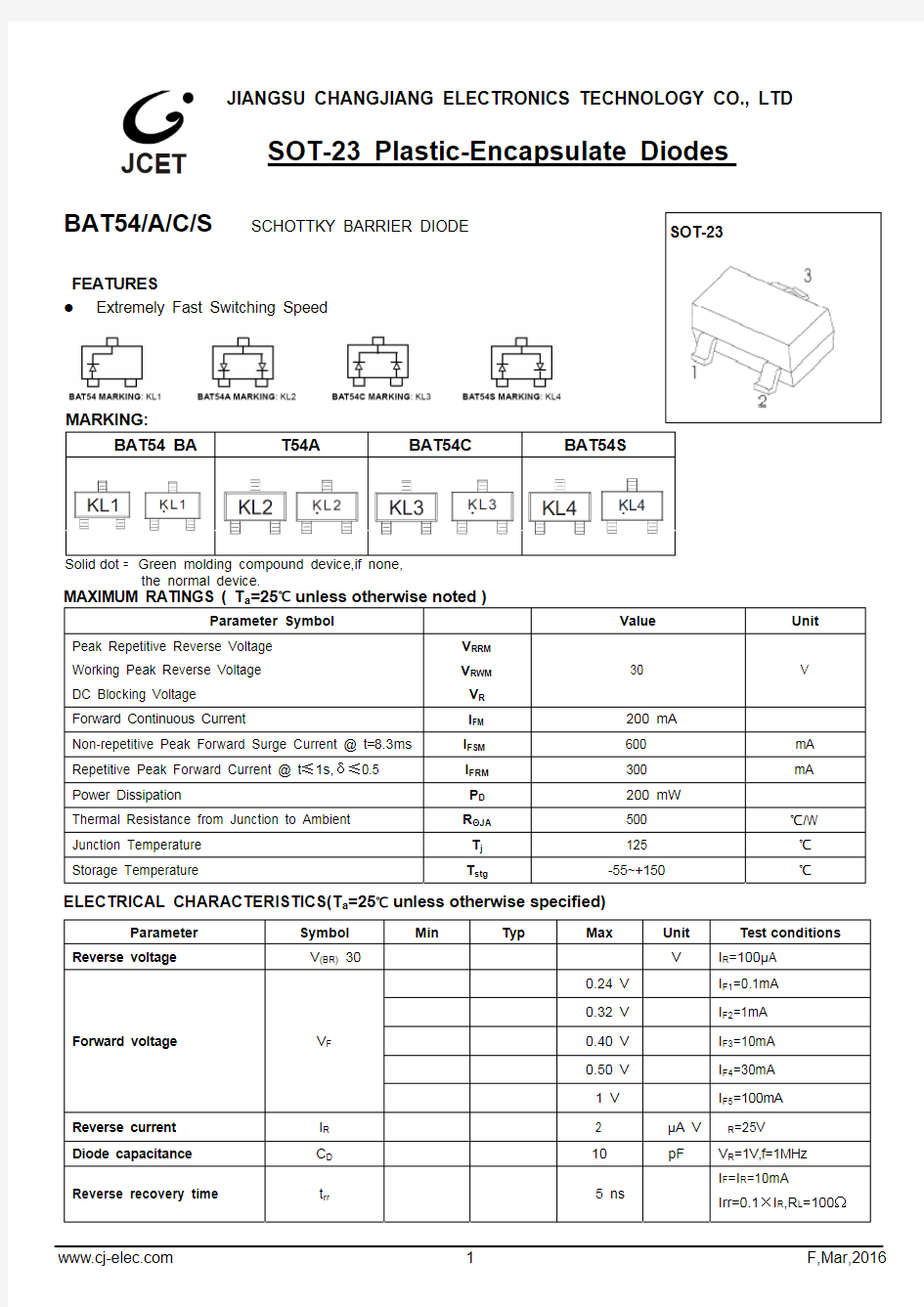
SOT-23
MARKING:
BA T54 BA T54A BA T54C
BA T54S
Solid
dot = Green molding compound device,if none, the normal device.
0255075100125
50
100
150
200
250
Capacitance Characteristics
REVERSE VOLTAGE V R (V)
C A P A C I T A N C E B E T W E E N T E R M I N A L S C T (p F )
Power Derating Curve
P O W E R D I S S I P A T I O N P D (m W )
AMBIENT TEMPERATURE T a ()
℃FORWARD VOLTAGE V F (mV)REVERSE VOLTAGE V R (V)
SO T -23 Package Outline Dimensions
SO T -23Suggested Pad Layout
RS1G快速恢复二极管规格书
(RS1A~RS1M) SMA A Fast Recovery rectifiers Major Ratings and Characteristics I F(AV) 1.0 A V RRM50 V to 1000 V I FSM30 A t rr150nS, 250nS, 500nS V F 1.3 V T j max.150 °C Features ●Low profile package ●Ideal for automated placement ●Glass passivated chip junction ●Fast switching for high efficiency ●High forward surage capability ●High temperatrue soldering: 260℃/10 seconds at terminals ●Component in accordance to RoHS 2002/95/1 and WEEE 2002/96/EC Mechanical Date ●Case: JEDEC DO-214AC molded plastic over glass passivated chip ●Terminals: Solder plated, solderable per J-STD-002B and JESD22-B102D ●Polarity: Laser band denotes cathode end Maximum Ratings & Thermal Characteristics & Electrical Characteristics (TA = 25 °C unless otherwise noted) Symbol(RS1A)(RS1B)(RS1D)(RS1G)(RS1J)(RS1K)(RS1M)UNIT Maximum repetitive peak reverse voltage V RRM501002004006008001000V Maximum RMS voltage V RMS3570140280420560700V Maximum DC blocking voltage V DC501002004006008001000V Maximum average forward rectified current I F(AV)1A Peak forward surge current 8.3 ms single half sine-wave superimposed on rated load I FSM30A Maximum instantaneous forwad voltage at 1.0V F 1.3V Maximum DC reverse current T A = 25 ℃at Rated DC blocking voltage T A = 125℃I R 5.0μA 50μA Maximum reverse recovery time at I F = 0.5 A , I R = 1.0 A , I rr = 0.25 A t rr150250500nS Typical junction capacitance at 4.0 V ,1MHz C J118pF Thermal resistance from junction to ambient RθJA75℃/ W Operating junction and storage temperature range T J,T STG–55 to +150 ℃- 1 - https://www.360docs.net/doc/cb413991.html,
TDK贴片电容型号选型规格书
C1005X5R1A475KTJ00E0402 X5R 10V 4.5UF 10% C1005X5R1E224KT000E0402 X5R 25V 220NF 10% C1005X5R1E225KT000E0402 X5R 25V 2.2UF 10% C1005X7R1C104KT000F0402 X7R 16V 100NF 10% C1005X7R1C224kT000E0402 X7R 16V 220NF 10% C1005X7R1H104KT000F0402 X7R 50V 100NF 10% C1608C0G1E103JT000N0603 C0G 25V 10NF 5% C1608C0G1H101JT000N0603 C0G 50V 100PF 5% C1608C0G1H152JT000N0603 C0G 50V 1.5NF 5% C1608C0G1H221JT000N0603 C0G 50V 220PF 5% C1608C0G1H222JT000N 0603 C0G 50V 2.2NF 5% C1608C0G1H472JT000N0603 C0G 50V 4.7NF 5% C1608C0G1H562JT000N0603 C0G 50V 5.2NF 5% C1608X5R0J106MTJ00N0603 X5R 6.3V 10UF 20% C1608X5R0J225KT000N0603 X5R 6.3V 2.2UF 10% C1608X5R0J226MT000N0603 X5R 6.3V 22UF 20% C1608X5R0J335KT000N0603 X5R 6.3V 3.3UF 10% C1608X5R0J475KT000N0603 X5R 6.3V 4.7UF 10% C1608X5R1A105KTJ00N0603 X5R 10V 1UF 10% C1608X5R1A106MT000E0603 X5R 10V 10UF 20% C1608X5R1A225KT000E0603 X5R 10V 2.2UF 10% C1608X5R1A226MTE00E0603 X5R 10V 22UF 20% C1608X5R1A475KT000N0603 X5R 10V 4.7UF 10% C1608X5R1C225KT000N0603 X5R 16V 2.2UF 10%
威世二极管规格书
SMBJ5.0 thru SMBJ188CA Vishay General Semiconductor Document Number: 88392For technical questions within your region, please contact one of the following:https://www.360docs.net/doc/cb413991.html, Surface Mount T RANS Z ORB ? Transient Voltage Suppressors FEATURES ?Low profile package ?Ideal for automated placement ?Glass passivated chip junction ? ?cycle): 0.01 % ?Excellent clamping capability ?Very fast response time ?Low incremental surge resistance ?Meets MSL level 1, per J-STD-020, LF maximum peak of 260 °C ?Solder dip 260 °C, 40 s ?Component in accordance to RoHS 2002/95/EC and WEEE 2002/96/EC TYPICAL APPLICATIONS Use in sensitive electronics protection against voltage transients induced by inductive load switching and lighting on ICs, MOSFET, signal lines of sensor units for consumer, computer, industrial, automotive and telecommunication. MECHANICAL DATA Case: DO-214AA (SMBJ) Molding compound meets UL 94 V-0 flammability rating Base P/N-E3 - RoHS compliant, commercial grade Base P/NHE3 - RoHS compliant, high reliability/automotive grade (AEC Q101 qualified) Terminals: Matte tin plated leads, solderable per J-STD-002 and JESD22-B102 E3 suffix meets JESD 201 class 1A whisker test, HE3suffix meets JESD 201 class 2 whisker test Polarity: For uni-directional types the band denotes cathode end, no marking on bi-directional types DEVICES FOR BI-DIRECTION APPLICATIONS For bi-directional devices use C or CA suffix (e.g. SMBJ10CA). Electrical characteristics apply in both directions. PRIMARY CHARACTERISTICS V WM 5.0 V to 188 V P PPM 600 W I FSM (uni-directional only) 100 A T J max. 150 °C DO-214AA (SMB J-Bend) Notes: (1) Non-repetitive current pulse, per Fig. 3 and derated above T A = 25 °C per Fig. 2(2) Mounted on 0.2 x 0.2" (5.0 x 5.0 mm) copper pads to each terminal MAXIMUM RATINGS (T A = 25°C unless otherwise noted) PARAMETER SYMBOL VALUE UNIT Peak pulse power dissipation with a 10/1000 μs waveform (1)(2) (Fig. 1) P PPM 600 W Peak pulse current with a 10/1000 μs waveform (1) I PPM See next table A Peak forward surge current 8.3 ms single half sine-wave uni-directional only (2) I FSM 100 A Operating junction and storage temperature range T J , T STG - 55 to + 150 °C
LED产品规格书
珠海市宏科光电子有限公司
产品规格书
样品单号:XY1704008
客户名称: 产品型号: HK-XB002ST12E-30(E2)
地址:珠海市金鼎镇拱星路 102 号 电话:+86-756-3382828/3810386 E-mail:sales@https://www.360docs.net/doc/cb413991.html, 传真:+86-756-3380859 https://www.360docs.net/doc/cb413991.html,
1
珠海市宏科光电子有限公司
■ 产品特点 1、可自由搭配和组合,组装方便 2、可靠性高,无闪灯,无斑块 3、高显指高光效,低热阻 4、散热好寿命长 5、节能环保
■ 产品应用 主要应用于 LED 射灯、LED 筒灯、LED 轨道灯、LED 舞台灯、LED 球泡灯、 LED 景观灯等家居及高空照明场所.
宏科 COB 光源是一款革命性、高效能,使用安装方便,降低灯具安装成 本、性能稳定的光源。COB 光源具有低运行温度、提高产品功率密度和可靠 性,延长光源使用寿命。为中功率集成封装低热阻,具有高光通量,高显色 性,高光效利用率等特性。
2
珠海市宏科光电子有限公司
■ 产品命名规则
产品系列:XB Series 承认日期:2018.05.04 版 本:1.0Page B 002 S T 12 E 30 (E2)
HK - X
注:1、显指代码 CIR
B:70 以下
C=70
E=80
G=90
H=95
2、色温代码: 27=2700K 30=3000K
40=4000K ……
3、发光颜色: W:白色(5000K 以上), N:中性白(3800K-5000K), S:暖白(3800K 以下) 4、封装工艺: B:常规耐温工艺 P:快速热疏通工艺 T:超高耐温工艺 C.专属光色工艺
3
贴片电阻规格 封装 尺寸
贴片电阻规格、封装、尺寸 ChipR Dimensions 、Footprint 简述 基本结构 分类 规格、封装、 尺寸 额定功率及工 作电压 阻值,标准阻 值 标识 规格书、生产 厂家
命名方法 价格、报价 创建时间:2005-12-30 最后修改时间:2006-10-29 贴片电阻套件 为方便学生、研发人员试验和产 品试制,特推出片式电阻系列套 件。 我们常说的贴片电阻 (SMD Resistor)叫"片式固定电阻器"(Chip Fixed Resistor),又叫"矩形片状电阻"(Rectangular Chip Resistors),是由ROHM 公司发明并最早推出市场的。特点是耐潮湿,耐高温,可靠度高,外观尺寸均匀,精确且温度系数与阻值公差小。 按生产工艺分厚膜(Thick Film Chip Resistors)、薄膜(Thin Film Chip Resistors )两种。厚膜是采用丝网印刷将电阻性材料淀积在绝缘基体(例如玻璃或氧化铝陶瓷)上,然后烧结形成的。我们通常所见的多为厚膜片式电阻,精度范围±0.5% ~ 10%,温度系数:±50PPM/℃~ ±400PPM/℃。薄膜是在真空中采用蒸发和溅射等工艺将电阻性材料淀积在绝缘基体工艺(真空镀膜技术)制
成,特点是低温度系数(±5PPM/℃),高精度(±0.01%~±1%)。 封装有:0201,0402,0603,0805,1206,1210,1812,2010,2512。其常规系列的精度为5%,1%。阻值范围从0.1欧姆到20M欧姆。标准阻值有E24,E96系列。功率有1/20W、1/16W、1/8W、1/10W、1/4W、1/2W、1W。 特性: 体积小,重量轻 适合波峰焊和回流焊 机械强度高,高频特性优越 常用规格价格比传统的引线电阻还便宜 生产成本低,配合自动贴片机,适合现代电子产品规模化生产使用状况:由于价格便宜,生产方便,能大面积减少PCB面积,减少产品外观尺寸,现在已取代绝大部分传统引线电阻。除一些小厂或不得不使用引线电阻的设计,各种电器上几乎都在使用。目前绝大部分电子产品,以0603、0805器件为主;以手机,PDA为代表的高密度电子产品多使用0201、0402的器件;一些要求稳定和安全的电子产品,如医疗器械、汽车行驶记录仪、税控机则多采用1206、1210等尺寸偏大的电阻。 市场状况:目前,在全球的市场份额中,排名依次是台湾、日本、中国、韩国,欧美几乎不再生产。主要的生产厂商几乎都在中国建立生产基地。台湾国巨(Yageo)公司为世界上第一大生产商。日本企业则生产一些如0201、0402、高精度、高电压,具有工艺难度,利润高的系列。台湾及国内工厂则多生产些
通用型贴片电容规格书(选型手册)
【 南京南山半导体有限公司 — 贴片电容选型资料】
https://www.360docs.net/doc/cb413991.html,
MULTILAYER CHIP CERAMIC CAPACITOR
COG/COH
COG
, ,
-55
125
,
0
30ppm/
0
60ppm/
0805
CG
101
J
500
N
T
(PF) ( 0402 0.04 0603 0.06 0805 0.08 1206 0.12 ) 0.02 0.03 0.05 0.06 1.00 1.60 2.00 3.20 ( ) 0.50 0.80 1.25 1.60 CG CH COG NPO COH 100 101 102 10 10
0 1
J G C B D
5.00% 2.00% 0.25PF 0.10PF 0.50PF
10 10 10 10
2
6R3 100 250 500
6.3V 10V 25V 50V
S C N / / T B
WB
W
T
L mm L 0402 0603 0805 1206 1005 1608 2012 3216 1.00 1.60 2.00 3.20 0.05 0.10 0.20 0.30 W 0.50 0.80 1.25 1.60 0.05 0.50 0.10 0.80 0.20 0.80 1.00 1.25 0.20 0.80 1.00 1.25 T WB 0.05 0.25 0.10 0.30 0.20 0.50 0.20 0.20 0.20 0.60 0.20 0.20 0.10 0.10 0.20 0.30
15
DSS120二极管规格书(星海)
DSS12 THRU DSS120 SURFACE MOUNT SCHOTTKY BARRIER RECTIFIER Reverse Voltage - 20 to 200 Volts Forward Current - 1.0 Ampere Case : JEDEC SOD-123FL molded plastic body Terminals : S olderable per MIL-STD-750,Method 2026 Polarity : Color band denotes cathode end Mounting Position : Any Weight :0.0007 ounce, 0.02 grams FEATURES MECHANICAL DATA MAXIMUM RATINGS AND ELECTRICAL CHARACTERISTICS Ratings at 25 C ambient temperature unless otherwise specified. Single phase half-wave 60Hz,resistive or inductive load,for capacitive load current derate by 20%. The plastic package carries Underwriters Laboratory Flammability Classification 94V-0 Metal silicon junction,majority carrier conduction Low power loss,high efficiency High forward surge current capability High temperature soldering guaranteed: 250 C/10 seconds,0.375”(9.5mm) lead length,5 lbs. (2.3kg) tension DSS12D12SYMBOLS UNITS DSS110D110 Note:1.Measured at 1MHz and applied reverse voltage of 4.0V D.C. 201420 V RRM V RMS V DC I (AV)I FSM V F 1.025.0 0.70 Operating junction temperature range Maximum repetitive peak reverse voltage Maximum RMS voltage Maximum DC blocking voltage Maximum average forward rectified current Peak forward surge current 8.3ms single half sine-wave superimposed on rated load (JEDEC Method) Maximum instantaneous forward voltage at 1.0A Maximum DC reverse current T A =25 C at rated DC blocking voltage T A =100 C Typical junction capacitance (NOTE 1)I R 0.5 C J T J T STG 80 Storage temperature range DSS13D13DSS15 D15 DSS14 D14 DSS16D16 DSS18D18DSS17D17 DSS19D19302130 402840 503550 604260 805680 10070100 704970 906390 VOLTS VOLTS VOLTS Amp Amps Volts pF C mA C -65 to +150-65 to +125 -65 to +15010.0 5.00.55 0.95110 SOD-123FL Dimensions in millimeters DSS115D115150105150 DSS120D120 200140200 0.85 0.22.0
LED投光灯规格书技术参数
LED 投光灯规格书 客户代码: 品名: LED 150W投光灯 规格: L425 * W325 * H190 mm 送样日期: 2014年6月30日 本厂型号: HTG06150 档案号: 送样数量: 承认书份数: 1份 一.产品材质: 高纯度铝制反射器,灯壳及散热体;高强度钢化玻璃罩;大功率LED 光源;搭配高效率恒流电源. 二.适用场所: 主要用于户外投光照明、建筑物外墙、港口码头等,户外广告。厂区、体育馆、停车场、广场、码头、工地、广告牌、桥梁、江河堤岸、园林、景观、庭院、草坪、池塘以及其他夜景亮化、照明的场所。 三、特点: 1.采用集成大功率LED(50W)作为光源。运用独特的多颗芯片集成式单模组光源设计,选用进口高亮度半 导体晶片。 2.散热器与灯壳一体化设计,LED 直接与外壳紧密相接,通过外壳散热翼与空气对流散热,充分保证了LED 灯的使用寿命。 3.灯壳采用铝合金压铸成型,可以有效的散热和防水、防尘。灯具表面进行了耐紫外线抗腐蚀处理,整体 灯具达到P65 标准。 4.采用单体椭圆反射腔配合球状弧面来设计,针对性地将LED 发出的光控制在需要的范围内,提高了灯具 出光效果的均匀性和光能的利用率,更能凸显LED泛光灯节能优点。与传统的纳灯相比,可节电70%以上. 5.无不良眩光、无频闪。消除了普通灯不良眩光引起的刺眼、视觉疲劳与视线干扰。 6.启动无延时,通电即亮,无需等待,消除了传统灯具长时间的启动过程。 7.绿色环保无污染,不含铅、汞等污染元素,对环境没有任何污染。
四、投光灯技术参数 五、使用说明 1.产品使用工作电压:AC 85V~265V 50/60Hz。勿超出工作电压范围。 2.贮存环境温度-50℃~+50℃.工作环境温度:-40℃~+50C℃,最佳工作环境温度为-0℃~+30℃。 3.由于灯具有玻璃配件,在搬运,贮存的时候请注意轻拿轻放,勿重压。
国巨电容规格
电容命名规则及采购信息要求 (一)国巨贴片电容的命名: 贴片电容的命名所包含的参数有贴片电容的尺寸、容值精度、贴片电容的材质、电压、电容容量、端头材料以及包装要求。 例国巨贴片电容CC0805JRNPO9BN101 CC:表示国巨电容系列名称——多层陶瓷贴片电容。国巨电容的系列 还有CA(表示排容),CH(表示高频电容)等等。 0805:表示尺寸,长度为0.08英寸,宽度为0.05英寸。此外,常见 的电容尺寸还有0201,0402,0603,1206,1210,1808,1812等。 J:表示电容容量的误差精度为±5%;另外B=±0.1PF,C=±0.25PF,D= ±0.5PF,F=±1PF,G=±2PF,K=±10%,M=±20%,Z=-20%~+80%。 R:表示7寸盘纸带包装。 NPO:表示电容材质。此外,常用的电容材质还有X5R,X7R,Y5V。 9:表示电压为50V。4=4V, 5=6.3V, 6=10V, 7=16V, 8=25V, 0=100V, A=200V, B=500V, C=1KV, D=2KV, E=3KV等(注意:100V是用数字0 表示,不是字母O) B:表示端头材料是镍电极。 N:表示NPO。 101:表示容值,前面两个数字为有效数字,第三个数字表示有几个 零。101=100PF, 102=1000PF, 103=10,000PF……以此类推。
(二)贴片电容的尺寸表示方法 贴片电容的尺寸表示法有两种,一种是以英寸为单位来表示,一种是以毫米为单位来表示。以英寸为单位来表示的称为英制尺寸,以毫米为单位来表示的称为公制尺寸。国巨贴片电容通常用英制尺寸来表示。
T4贴片二极管规格书
BAV16W/1N4148W FAST SWITHING DIODES FEATURES MECHANICAL DATA Fast switching speed Surface mount package ideally suited for automatic insertion For general purpose switching applications High conductance MAXIMUM RATINGS AND ELECTRICAL CHARACTERISTICS 3001502.01.0400315125-65 to +150 100 Maximum ratings and electrical characteristics, Single diode @T A =25C V SYMBOLS UNITS V RRM V RWM V R Peak repetitive peak reverse voltage Working peak DC Blocking voltage RMS Reverse voltage Forward continuous current Average rectified output current Peak forward current @=1.0u s @=1.0s Power dissipation Thermal resistance junction to ambient Junction temperature Storage temperature Non-Repetitive peak reverse voltage T j T STG V RM V mA mA A mW K/W C C V Limits 7553V R(RMS)I FM I O Pd Electrical ratings @T A =25C PARAMETER I FSM R ΘJA Case : Molded plastic body Terminals : Plated leads solderable per MIL-STD-750, Method 2026 Polarity : Polarity symbols marked on case Marking :T6, T4 SOD-123 Dimensions in millimeters and (inches)
(完整版)贴片电容的介绍
X7R 性质: 1. 介电常数可达到3000,容温变化率小于15%,介电损耗小于3.5%; 2. 粉体粒径250-300nm,烧成陶瓷晶粒尺寸300-400nm。 电镜照片: 用途: 1. 此介质材料为环保型粉料,无任何有毒镉(Cd)和铅(Pd)的化合物; 2. 适合于制备超薄层大容量贱金属内电极多层陶瓷电容器的生产:单层陶瓷膜片厚度5~10mm;层数从几十到几百层;电容量从 0.1 nF 到100 nF; 3. 由于瓷粉粒度小,分散性好,因此不需要再进行剧烈的球磨,以免改变瓷料的晶粒性质,使性能劣化。 Y5V贴片电容,MLCC Y5V多层陶瓷片式电容 贴片电容简述 COG(NPO)贴片电容选型表 X7R贴片电容选型表 创建时间:2006-1-13 最后修改时间:2006-1-13 简述 Y5V贴片电容属于EIA规定的Class 2类材料的电容。它的电容量受温度、电压、时间变化影响大。
Y5V贴片电容特性 ?具有较差的电容量稳定性,在-25℃~85℃工作温度范围内,温度特性为+30%,-80%。 ?层叠独石结构,具有高可靠性。 ?优良的焊接性和和耐焊性,适用于回流炉和波峰焊。 ?应用于温度变化小的退耦、隔直等电路中。 Y5V贴片电容各个生产厂家规格书 生产厂家规格书 AVX Datasheet 风华Datasheet 国巨Datasheet 太阳诱电Datasheet 村田Datasheet Y5V贴片电容容量范围 厚度与符号对应表 符 号 A C E G J K M N P Q X Y Z 最 大 厚 度毫米(英寸) 0.33 (0.013 ) 0.56 (0.022 ) 0.71 (0.028 ) 0.86 (0.034 ) 0.94 (0.037 ) 1.02 (0.040 ) 1.27 (0.050 ) 1.40 (0.055 ) 1.52 (0.060 ) 1.78 (0.070 ) 2.29 (0.090 ) 2.54 (0.100 ) 2.79 (0.110 ) 0201~1210 Y5V贴片电容选型表 封装尺寸0201 0402 0603 0805 1206 1210 工作电压6. 3 1 6. 3 1 1 6 2 5 5 6. 3 1 1 6 2 5 5 6. 3 1 1 6 2 5 5 6. 3 1 1 6 2 5 5 6. 3 1 1 6 2 5 5 电容量(pF ) 820 1000 2200 4700 A A A C 电容量(uF 0.01 0.02 2 A A A A C C C C C G G G G
发光二极管产品规格书(精)
发光二极管产品规格书 发光二极管产品规格书 型号 : H2B01ARD04 注意谨防静电! 制作核准顾客 Page 1 of 4 Created with novaPDF Printer (https://www.360docs.net/doc/cb413991.html,). Please register to remove this message. H2B01ARD04 文件编号: BF-2005-03-040 产品特征 直径为3mm圆型 高亮红色,低功耗 外观为有色散射 产品应用 各类仪表指示光源 小区域 产品外型图 注: 所有的尺寸单位为毫米(mm),公差为 0.20mm 产品指南 光强Iv(mcd)@20mA 型号发光颜色芯片材料胶体颜色 Min. Typ. Max. 半功率角度 2θ1/2 H2B01ARD04 红色 ALGaAs 有色散射 40 60 --- 60 注: 中心轴亮度50%时单边的发光角度为θ1/2, 2θ1/2=θ1/2+θ1/2 Page 2 of 4 Created with novaPDF Printer (https://www.360docs.net/doc/cb413991.html,). Please register to remove this message. H2B01ARD04 文件编号: BF-2005-03-040 最大限度性能参数(Ta=25℃) 项目符号最大限度单位 功率消耗 PD 80 mW 峰值正向电流 1/10占空比 0.1ms 脉宽 IFP 100 mA 正向电流 IF 20 mA 反向电压 VR 5 V 工作温度 Topr -25℃~+80℃ 储存温度 Tstg -25℃~+100℃ 焊接温度Tsol 260℃下5秒
国巨电容规格书
1. SUBJECT: This specification applies on the chip capacitor made by Yageo Corporation. 2. PART NUMBER: Part number of the chip capacitor is identified by the size, tolerance, packing, material and capacitor value. Example:
3. ELECTRICAL CHARACTERISTICS
4. DIMENSION (mm) L W T L 1;L 2 L 3 Style MIN. MAX. MIN. MAX. Min. CC0402 1.0±0.05 0.5±0.05 0.45 0.55 0.15 0.30 0.40 CC0603 1.6±0.10 0.8±0.10 0.70 0.90 0.20 0.60 0.40 CC0805 2.0±0.10 1.25±0.10 0.50 1.35 0.25 0.75 0.55 CC1206 3.2±0.15 1.6±0.15 0.50 1.35 0.25 0.75 1.40 CC1210 3.2±0.20 2.5±0.20 0.50 1.80 0.25 0.75 1.40 CC1812 4.5±0.20 3.2±0.20 0.50 1.80 0.25 0.75 2.20 CC2220 5.7±0.20 5.0±0.20 0.50 1.80 0.25 0.75 2.20 Unit: mm
ES1GL二极管规格书(常州星海)
SURFACE MOUNT SUPER FAST RECTIFIER Reverse Voltage - 50 to 600 Volts Forward Current - 1.0 Ampere Case : JEDEC SOD-123FL molded plastic body over passivated chip Terminals : Plated axial leads, solderable per MIL-STD-750,Method 2026 Polarity : Color band denotes cathode end Mounting Position : Any Weight :0.0007 ounce, 0.02 grams Glass passivated device Ideal for surface mouted applications FEATURES MECHANICAL DATA MAXIMUM RATINGS AND ELECTRICAL CHARACTERISTICS ES1BL SYMBOLS UNITS Metallurgically bonded construction High temperature soldering guaranteed: 260 C/10 seconds,0.375”(9.5mm) lead length,5 lbs. (2.3kg) tension Low reverse leakage 10070100400280400150105150600420600 VOLTS VOLTS VOLTS Amp Amps Volts V RRM V RMS V DC I (AV) I FSM V F 1.0 25.0 1.25 Maximum repetitive peak reverse voltage Maximum RMS voltage Maximum DC blocking voltage Maximum average forward rectified current Peak forward surge current 8.3ms single half sine-wave superimposed on rated load (JEDEC Method) Maximum instantaneous forward voltage at1.0A Maximum DC reverse current T A =25 C at rated DC blocking voltage T A =100 C I R 5.0100.0A μRatings at 25 C ambient temperature unless otherwise specified. Single phase half-wave 60Hz,resistive or inductive load,for capacitive load current derate by 20%. ES1AL THRU ES1JL ES1CL ES1DL ES1EL ES1JL EB EC ED EE EJ EG ES1GL Maximum reverse recovery time (NOTE 1)Typical junction capacitance (NOTE 2) C J pF ELECTRONICS CO.,LTD. STAR SEA Operating junction and storage temperature range Note:R θJA T J ,T STG 8510-55 to +150 C Typical thermal resistance (NOTE 3)K/W 2.Measured at 1MHz and applied reverse voltage of 4.0V D.C.1.Measured with IF=0.5A, IR=1A, Irr=0.25A. 3.PCB mounted on 0.2*0.2" (5.0*5.0mm) coppeer pad area. 35ns 503550EA ES1AL trr 200140200 3002103000.95 1.7 SOD-123FL Dimensions in millimeters
DSR1M二极管规格书(常州星海)
SUFACE MOUNT GENERAL PURPOSE SILICON RECTIFIER Reverse Voltage - 50 to 1000 Volts Forward Current - 1.0 Ampere Case : JEDEC SOD-123FL molded plastic body over passivated chip Terminals : S olderable per MIL-STD-750,Method 2026 Polarity : Color band denotes cathode end Mounting Position : Any Weight :0.006 ounce, 0.02 grams Glass passivated device Ideal for surface mouted applications FEATURES MECHANICAL DATA MAXIMUM RATINGS AND ELECTRICAL CHARACTERISTICS Metallurgically bonded construction High temperature soldering guaranteed: 250 C/10 seconds,0.375”(9.5mm) lead length,5 lbs. (2.3kg) tension Low reverse leakage Note: 3.Thermal resistance from junction to ambient at 0.375” (9.5mm)lead length,P.C.B. mounted ELECTRONICS CO.,LTD. LING JIE STAR SEA Ratings at 25 C ambient temperature unless otherwise specified. Single phase half-wave 60Hz,resistive or inductive load,for capacitive load current derate by 20%. DSR1A THRU DSR1M 2.Measured at 1MHz and applied reverse voltage of 4.0V D.C. 1.Averaged over any 20ms period. DSR1B SYMBOLS 10070100400280400200140200 600420600800560800 V RRM V RMS V DC I (AV) I FSM V F 1.0 25.01.1Operating junction and storage temperature range Maximum repetitive peak reverse voltage Maximum RMS voltage Maximum DC blocking voltage Maximum average forward rectified current at T A =65 C (NOTE 1) Peak forward surge current 8.3ms single half sine-wave superimposed on rated load (JEDEC Method)Maximum instantaneous forward voltage at 1.0A Maximum DC reverse current T A =25 C at rated DC blocking voltage T A =125 C Typical junction capacitance (NOTE 2)I R 10.050.0R θJA C J T J ,T STG 1804-55 to +150 Typical thermal resistance (NOTE 3) UNITS VOLTS VOLTS VOLTS Amp Amps Volts pF C A μK/W DSR1D DSR1G DSR1J DSR1K S1B S1D S1G S1J S1K T L =25 C 503550S1A DSR1A 10007001000 DSR1M S1M SOD-123FL Dimensions in millimeters