MAC223A8中文资料
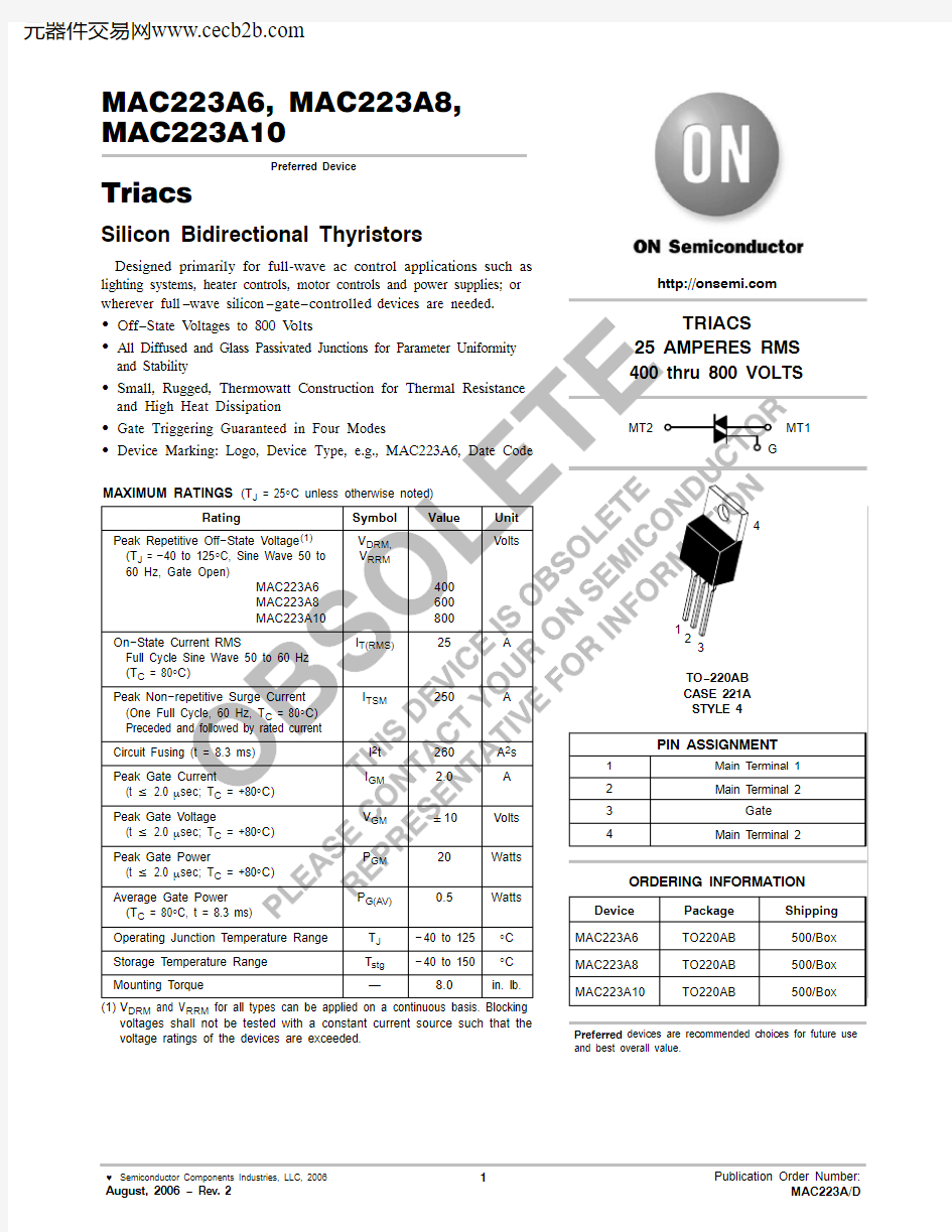
MAC223A6, MAC223A8, MAC223A10
Preferred Device
Triacs
Silicon Bidirectional Thyristors
Designed primarily for full-wave ac control applications such as lighting systems, heater controls, motor controls and power supplies; or
voltages shall not be tested with a constant current source such that the voltage ratings of the devices are exceeded.
TRIACS
25 AMPERES RMS
400 thru 800 VOLTS
Device Package Shipping
ORDERING INFORMATION
MAC223A6TO220AB500/Box MAC223A8TO220AB
MAC223A10TO220AB
TO?220AB
CASE 221A
STYLE 4
1
2
3
4
PIN ASSIGNMENT
1
2
3Gate
Main Terminal 1
Main Terminal 2
4Main Terminal 2
https://www.360docs.net/doc/c71910731.html,
500/Box
500/Box
MT1
G
MT2
Preferred devices are recommended choices for future use and best overall value.
THERMAL CHARACTERISTICS
Characteristic Symbol Value Unit Thermal Resistance, Junction to Case RθJC 1.2°C/W Thermal Resistance, Junction to Ambient RθJA60°C/W Maximum Lead T emperature for Soldering Purposes 1/8″ from Case for 10 Seconds T L260°C
ELECTRICAL CHARACTERISTICS (T C = 25°C unless otherwise indicated; Electricals apply in both directions)
Characteristic Symbol Min Typ Max Unit OFF CHARACTERISTICS
Peak Repetitive Blocking Current T J = 25°C (V D = Rated V DRM,V RRM;Gate Open)T J = 125°C I DRM,
I RRM
—
—
—
—
10
2.0
μA
mA
ON CHARACTERISTICS
Peak On?State Voltage (I TM = "35 A Peak, Pulse Width v2 ms,
Duty Cycle v2%)
V TM— 1.4 1.85Volts
Gate Trigger Current (Continuous dc)
(V D = 12 V, R L = 100 Ω)
MT2(+), G(+); MT2(?), G(?); MT(+), G(?) MT2(?), G(+)I GT
—
—
20
30
50
75
mA
Gate Trigger Voltage (Continuous dc)
(V D = 12 V, R L = 100 Ω)
MT2(+), G(+); MT2(?), G(?); MT(+), G(?) MT2(?), G(+)V GT
—
—
1.1
1.3
2.0
2.5
Volts
Gate Non?trigger Voltage
(V D = 12 V, T J = 125°C, R L = 100 Ω) All Quadrants V GD
0.20.4—
Volts
Holding Current
(V D = 12 Vdc, Gate Open, Initiating Current = "200 mA)
I H—1050mA
Turn?On Time
(V D = Rated V DRM, I TM = 35 A Peak, I G = 200 mA)
t gt— 1.5—μs DYNAMIC CHARACTERISTICS
Critical Rate of Rise of Off-State Voltage
(V D = Rated V DRM, Exponential Waveform, T C = 125°C)
dv/dt—40—V/μs
Critical Rate of Rise of Commutation Voltage
(V D = Rated V DRM, I TM = 35 A Peak, Commutating
di/dt = 12.6 A/ms, Gate Unenergized, T C = 80°C)
dv/dt(c)— 5.0—V/μs
Voltage Current Characteristic of Triacs
(Bidirectional Device)
+ Current
All polarities are referenced to MT1.
With in?phase signals (using standard AC lines) quadrants I and III are used.
T , M A X I M U M A L L O W A B L E C A S E T E M P E R A T U R E ( C )
C °
N O R M A L I Z E D G A T E C U R R E N T
T J , JUNCTION TEMPERATURE (°C)V TM , INSTANTANEOUS ON?STATE VOLTAGE (VOLTS)
i N O R M A L I Z E D H O L D C U R R E N T
Figure 5. Typical Hold Current Figure 6. Typical On ?State Characteristics
PACKAGE DIMENSIONS
TO?220AB
CASE 221A?07
ISSUE Z
and are registered trademarks of Semiconductor Components Industries, LLC (SCILLC). SCILLC reserves the right to make changes without further notice to any products herein. SCILLC makes no warranty, representation or guarantee regarding the suitability of its products for any particular purpose, nor does SCILLC assume any liability
PUBLICATION ORDERING INFORMATION