2N7002-7-F中文资料
Features
? Low On-Resistance: R DS(ON) ? Low Gate Threshold Voltage ? Low Input Capacitance ? Fast Switching Speed
? Low Input/Output Leakage
? Lead Free/RoHS Compliant (Note 2)
?
Qualified to AEC-Q101 Standards for High Reliability
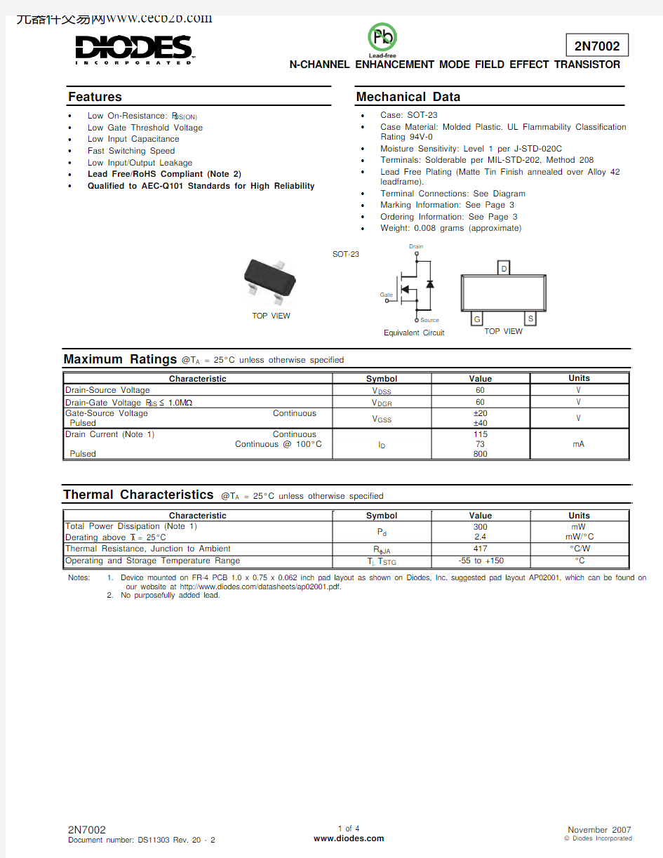
Mechanical Data
? Case: SOT-23
? Case Material: Molded Plastic. UL Flammability Classification Rating 94V-0
? Moisture Sensitivity: Level 1 per J-STD-020C
? Terminals: Solderable per MIL-STD-202, Method 208
? Lead Free Plating (Matte Tin Finish annealed over Alloy 42 leadframe).
? Terminal Connections: See Diagram ? Marking Information: See Page 3 ? Ordering Information: See Page 3 ?
Weight: 0.008 grams (approximate)
SOT-23
TOP VIEW
Equivalent Circuit
Maximum Ratings @T A = 25°C unless otherwise specified
Characteristic
Symbol Value
Units Drain-Source Voltage V DSS 60
V Drain-Gate Voltage R GS ≤ 1.0M Ω
V DGR
60 V Gate-Source Voltage Continuous Pulsed V GSS
±20
±40 V Drain Current (Note 1) Continuous Continuous @ 100°C Pulsed I D
115 73 800
mA
Thermal Characteristics @T A = 25°C unless otherwise specified
Characteristic Symbol Value Units Total Power Dissipation (Note 1) Derating above T A = 25°C
P d 300 2.4 mW mW/°C Thermal Resistance, Junction to Ambient R θJA 417 °C/W Operating and Storage Temperature Range
T j, T STG
-55 to +150 °C
Notes:
1. Device mounted on FR-4 PCB 1.0 x 0.75 x 0.062 inch pad layout as shown on Diodes, Inc. suggested pad layout AP02001, which can be found on our website at https://www.360docs.net/doc/cf12844357.html,/datasheets/ap02001.pdf.
2. No purposefully added lead.
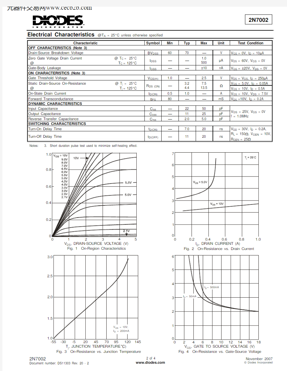
Electrical Characteristics @T A = 25°C unless otherwise specified
Characteristic Symbol Min Typ Max
Unit Test Condition OFF CHARACTERISTICS (Note 3) Drain-Source Breakdown Voltage BV DSS 60 70 ? V V GS = 0V, I D = 10μ
A Zero Gate Voltage Drain Current @ T C = 25°C @ T C = 125°C
I DSS
? ? 1.0
500 μA V DS = 60V, V GS = 0V Gate-Body Leakage I GSS ? ? ±10 nA V GS = ±20V, V
DS = 0V ON CHARACTERISTICS (Note 3) Gate Threshold Voltage V GS(th) 1.0 ? 2.5
V V DS = V GS , I D = 250μA V GS = 5.0V, I D = 0.05A Static Drain-Source On-Resistance @ T j = 25°C @ T j = 125°C R DS (ON)
? 3.2 4.4 7.5
13.5 Ω V GS = 10V, I D = 0.5A On-State Drain Current
I D(ON)0.5 1.0 ? A V GS = 10V, V DS = 7.5V Forward Transconductance
g FS 80 ? ? mS V DS =10V, I D = 0.2A DYNAMIC CHARACTERISTICS Input Capacitance C iss ? 22 50 pF Output Capacitance
C oss ? 11 25 pF Reverse Transfer Capacitance
C rss ? 2.0 5.0 pF V DS = 25V, V GS = 0V f = 1.0MHz
SWITCHING CHARACTERISTICS Turn-On Delay Time t D(ON)? 7.0 20 ns Turn-Off Delay Time
t D(OFF)
?
11
20
ns
V DD = 30V, I D = 0.2A, R L = 150Ω, V GEN = 10V, R GEN = 25Ω
Notes:
3. Short duration pulse test used to minimize self-heating effect.
V , DRAIN-SOURCE VOLTAGE (V)Fig. 1 On-Region Characteristics
DS I , D R A I N -S O U R C E C U R R E N T (A )
D
I , DRAIN CURRENT (A)
Fig. 2 On-Resistance vs. Drain Current D R , N O R M A L I Z E D D R A I N -S O U R C E O N -R E S I S T A N C E ()
D S (O N )Ω
T , JUNCTION TEMPERATURE (C)
Fig. 3 On-Resistance vs. Junction Temperature j °R , S T A T I C D R A I N -S O U R C E O N -R E S I S T A N C E ()
D S (O N )Ω V , GAT
E TO SOURCE VOLTAGE (V)
Fig. 4 On-Resistance vs. Gate-Source Voltage GS R , N O R M A L I Z E D D R A I N -S O U R C E O N -R E S I S T A N C E ()
D S (O N )Ω
V G A T E S O U R C E C U R R E N T (V )
G S ,I , DRAIN CURRENT (A)
Fig. 5 Typical Transfer Characteristics D
P , P O W E R D I S S I P A T I O N (m W )
d T , AMBIENT TEMPERATURE (C)
Fig. 6 Max Power Dissipation vs. Ambient Temperature A °
Ordering Information (Note 4)
Part Number Case Packaging 2N7002-7-F
SOT-23 3000/Tape & Reel
Notes: 4. For packaging details, go to our website at https://www.360docs.net/doc/cf12844357.html,/datasheets/ap02007.pdf.
Marking Information
K7x
Y M
K7x = Product Type Marking Code, e.g. K72 YM = Date Code Marking Y = Year ex: N = 2002
M = Month ex: 9 = September
Date Code Key
Year
1998 1999 2000 2001 2002200320042005 2006 2007 2008 2009 2010 2011 2012 Code
J K L
M N P R
S
T U V W X
Y Z
Month Jan
Feb
Mar
Apr
May
Jun
Jul
Aug
Sep
Oct
Nov
Dec
Code 1 2 3 4 5 6 7 8 9 O N D
Package Outline Dimensions
SOT-23
Dim Min Max A 0.37 0.51 B 1.20 1.40 C 2.30 2.50 D 0.89 1.03 F 0.45 0.60 G 1.78 2.05 H 2.80 3.00 J 0.013 0.10 K 0.903 1.10 L 0.45 0.61 M 0.085 0.180
α
0° 8° All Dimensions in mm
Suggested Pad Layout
IMPORTANT NOTICE
Diodes Incorporated and its subsidiaries reserve the right to make modifications, enhancements, improvements, corrections or other changes without further notice to any product herein. Diodes Incorporated does not assume any liability arising out of the application or use of any product described herein; neither does it convey any license under its patent rights, nor the rights of others. The user of products in such applications shall assume all risks of such use and will agree to hold Diodes Incorporated and all the companies whose products are represented on our website, harmless against all damages.
LIFE SUPPORT
Diodes Incorporated products are not authorized for use as critical components in life support devices or systems without the expressed written approval of the President of Diodes Incorporated.
X E
G
Y C
Z
Dimensions Value (in mm)
Z 3.4 G 0.7 X 0.9 Y 1.4 C 2.0 E 0.9