M93C46-RBN3中文资料

1/31
August 2004M93C86, M93C76, M93C66
M93C56, M93C46
16Kbit, 8Kbit, 4Kbit, 2Kbit and 1Kbit (8-bit or 16-bit wide)
MICROWIRE? Serial Access EEPROM
FEATURES SUMMARY
s Industry Standard MICROWIRE Bus s
Single Supply Voltage:
– 4.5 to 5.5V for M93Cx6– 2.5 to 5.5V for M93Cx6-W – 1.8 to 5.5V for M93Cx6-R
s Dual Organization: by Word (x16) or Byte (x8) s Programming Instructions that work on: Byte, Word or Entire Memory
s Self-timed Programming Cycle with Auto-Erase
s Ready/Busy Signal During Programming s
Speed:
–1MHz Clock Rate, 10ms Write Time
(Current product, identified by process identification letter F or M)
–2MHz Clock Rate, 5ms Write Time (New
Product, identified by process identification letter W or G or S) s Sequential Read Operation
s Enhanced ESD/Latch-Up Behaviour s More than 1 Million Erase/Write Cycles s
More than 40 Year Data Retention
Table 1. Product List
Reference
Part Number Reference
Part Number M93C86
M93C86
M93C56M93C56M93C86-W M93C56-W M93C86-R M93C56-R M93C76
M93C76
M93C46M93C46M93C76-W M93C46-W M93C76-R M93C46-R
M93C66
M93C66
M93C66-W M93C66-R
M93C86, M93C76, M93C66, M93C56, M93C46
TABLE OF CONTENTS
FEATURES SUMMARY . . . . . . . . . . . . . . . . . . . . . . . . . . . . . . . . . . . . . . . . . . . . . . . . . . . . . . . . . . . . .1
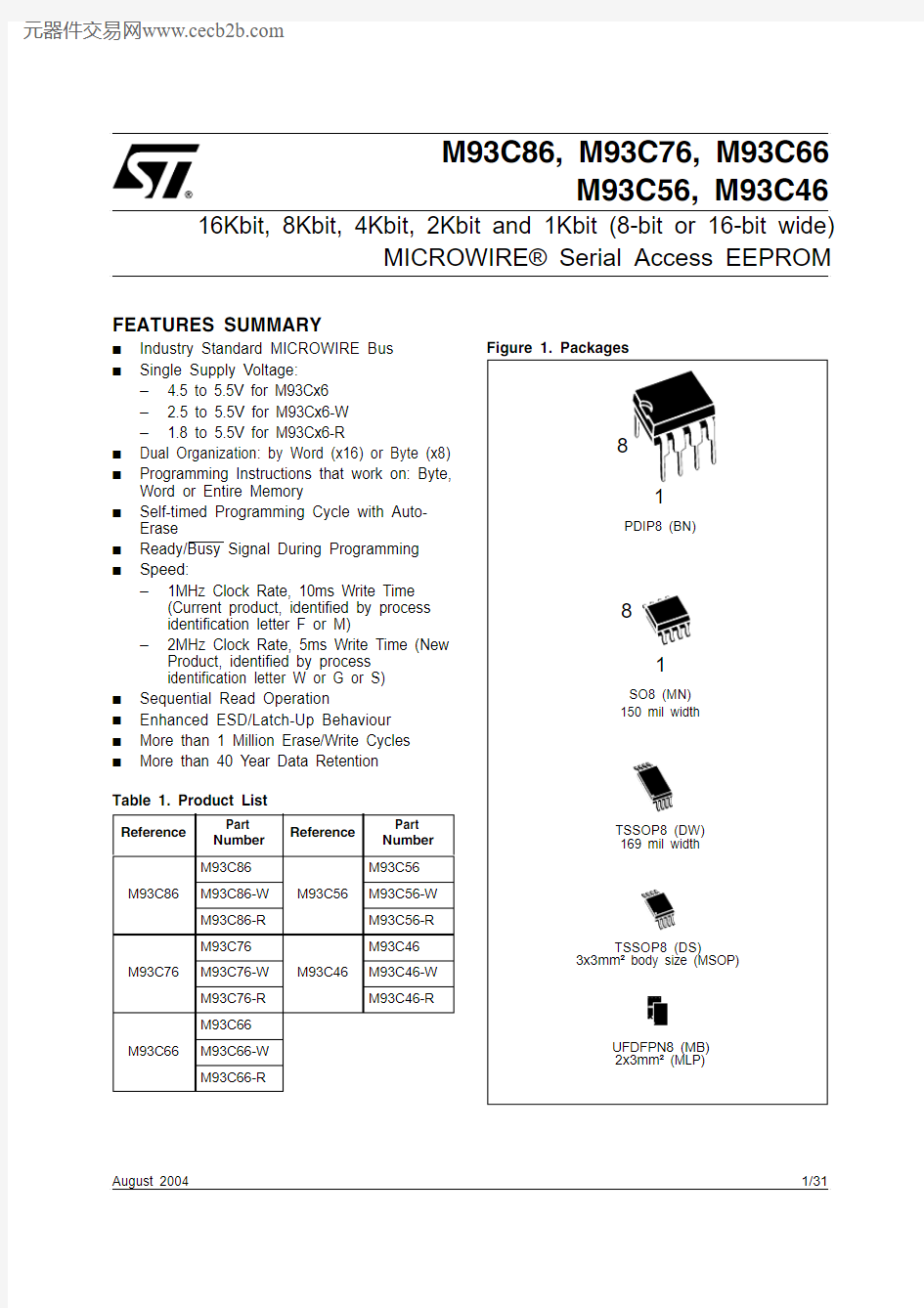
Table 1.Product List . . . . . . . . . . . . . . . . . . . . . . . . . . . . . . . . . . . . . . . . . . . . . . . . . . . . . . . . . . . .1 Figure 1.Packages. . . . . . . . . . . . . . . . . . . . . . . . . . . . . . . . . . . . . . . . . . . . . . . . . . . . . . . . . . . . . .1 Figure 2.Logic Diagram . . . . . . . . . . . . . . . . . . . . . . . . . . . . . . . . . . . . . . . . . . . . . . . . . . . . . . . . . .4 Table 2.Signal Names . . . . . . . . . . . . . . . . . . . . . . . . . . . . . . . . . . . . . . . . . . . . . . . . . . . . . . . . . .4 Table 3.Memory Size versus Organization. . . . . . . . . . . . . . . . . . . . . . . . . . . . . . . . . . . . . . . . . . .4 Table 4.Instruction Set for the M93Cx6 . . . . . . . . . . . . . . . . . . . . . . . . . . . . . . . . . . . . . . . . . . . . .4 Figure 3.DIP, SO, TSSOP and MLP Connections (Top View). . . . . . . . . . . . . . . . . . . . . . . . . . . . .5
MEMORY ORGANIZATION . . . . . . . . . . . . . . . . . . . . . . . . . . . . . . . . . . . . . . . . . . . . . . . . . . . . . . . . . .5 POWER-ON DATA PROTECTION. . . . . . . . . . . . . . . . . . . . . . . . . . . . . . . . . . . . . . . . . . . . . . . . . . . ..5
INSTRUCTIONS . . . . . . . . . . . . . . . . . . . . . . . . . . . . . . . . . . . . . . . . . . . . . . . . . . . . . . . . . . . . . . . . . . .6
Table 5.Instruction Set for the M93C46 . . . . . . . . . . . . . . . . . . . . . . . . . . . . . . . . . . . . . . . . . . . . .6 Table 6.Instruction Set for the M93C56 and M93C66 . . . . . . . . . . . . . . . . . . . . . . . . . . . . . . . . . .7 Table 7.Instruction Set for the M93C76 and M93C86 . . . . . . . . . . . . . . . . . . . . . . . . . . . . . . . . . .7 Read . . . . . . . . . . . . . . . . . . . . . . . . . . . . . . . . . . . . . . . . . . . . . . . . . . . . . . . . . . . . . . . . . . . . . . . . .8 Erase/Write Enable and Disable. . . . . . . . . . . . . . . . . . . . . . . . . . . . . . . . . . . . . . . . . . . . . . . . . . .8 Figure 4.READ, WRITE, EWEN, EWDS Sequences. . . . . . . . . . . . . . . . . . . . . . . . . . . . . . . . . . . .8 Erase. . . . . . . . . . . . . . . . . . . . . . . . . . . . . . . . . . . . . . . . . . . . . . . . . . . . . . . . . . . . . . . . . . . . . . . . .9 Write . . . . . . . . . . . . . . . . . . . . . . . . . . . . . . . . . . . . . . . . . . . . . . . . . . . . . . . . . . . . . . . . . . . . . . . . .9 Figure 5.ERASE, ERAL Sequences . . . . . . . . . . . . . . . . . . . . . . . . . . . . . . . . . . . . . . . . . . . . . . . .9 Erase All. . . . . . . . . . . . . . . . . . . . . . . . . . . . . . . . . . . . . . . . . . . . . . . . . . . . . . . . . . . . . . . . . . . . .10 Write All . . . . . . . . . . . . . . . . . . . . . . . . . . . . . . . . . . . . . . . . . . . . . . . . . . . . . . . . . . . . . . . . . . . . .10 Figure 6.WRAL Sequence. . . . . . . . . . . . . . . . . . . . . . . . . . . . . . . . . . . . . . . . . . . . . . . . . . . . . . .10
READY/BUSY STATUS . . . . . . . . . . . . . . . . . . . . . . . . . . . . . . . . . . . . . . . . . . . . . . . . . . . . . . . . . . . .11 COMMON I/O OPERATION . . . . . . . . . . . . . . . . . . . . . . . . . . . . . . . . . . . . . . . . . . . . . . . . . . . . . . . . .11
CLOCK PULSE COUNTER . . . . . . . . . . . . . . . . . . . . . . . . . . . . . . . . . . . . . . . . . . . . . . . . . . . . . . . . .11 Figure 7.Write Sequence with One Clock Glitch . . . . . . . . . . . . . . . . . . . . . . . . . . . . . . . . . . . . . .11
MAXIMUM RATING. . . . . . . . . . . . . . . . . . . . . . . . . . . . . . . . . . . . . . . . . . . . . . . . . . . . . . . . . . . . . . . .12 Table 8.Absolute Maximum Ratings. . . . . . . . . . . . . . . . . . . . . . . . . . . . . . . . . . . . . . . . . . . . . . .12
DC AND AC PARAMETERS. . . . . . . . . . . . . . . . . . . . . . . . . . . . . . . . . . . . . . . . . . . . . . . . . . . . . . . . .13 Table 9.Operating Conditions (M93Cx6) . . . . . . . . . . . . . . . . . . . . . . . . . . . . . . . . . . . . . . . . . . .13 Table 10.Operating Conditions (M93Cx6-W) . . . . . . . . . . . . . . . . . . . . . . . . . . . . . . . . . . . . . . . . .13 Table 11.Operating Conditions (M93Cx6-R) . . . . . . . . . . . . . . . . . . . . . . . . . . . . . . . . . . . . . . . . .13 Table 12.AC Measurement Conditions (M93Cx6) . . . . . . . . . . . . . . . . . . . . . . . . . . . . . . . . . . . . .14 Table 13.AC Measurement Conditions (M93Cx6-W and M93Cx6-R) . . . . . . . . . . . . . . . . . . . . . .14 Figure 8.AC Testing Input Output Waveforms. . . . . . . . . . . . . . . . . . . . . . . . . . . . . . . . . . . . . . . .14
2/31
M93C86, M93C76, M93C66, M93C56, M93C46
Table 14.Capacitance. . . . . . . . . . . . . . . . . . . . . . . . . . . . . . . . . . . . . . . . . . . . . . . . . . . . . . . . . . .14 Table 15.DC Characteristics (M93Cx6, Device Grade 6). . . . . . . . . . . . . . . . . . . . . . . . . . . . . . . .15 Table 16.DC Characteristics (M93Cx6, Device Grade 7 or 3) . . . . . . . . . . . . . . . . . . . . . . . . . . . .15 Table 17.DC Characteristics (M93Cx6-W, Device Grade 6) . . . . . . . . . . . . . . . . . . . . . . . . . . . . .16 Table 18.DC Characteristics (M93Cx6-W, Device Grade 7 or 3). . . . . . . . . . . . . . . . . . . . . . . . . .17 Table 19.DC Characteristics (M93Cx6-R) . . . . . . . . . . . . . . . . . . . . . . . . . . . . . . . . . . . . . . . . . . .17 Table 20.AC Characteristics (M93Cx6, Device Grade 6, 7 or 3) . . . . . . . . . . . . . . . . . . . . . . . . . .18 Table 21.AC Characteristics (M93Cx6-W, Device Grade 6). . . . . . . . . . . . . . . . . . . . . . . . . . . . . .19 Table 22.AC Characteristics (M93Cx6-W, Device Grade 7 or 3). . . . . . . . . . . . . . . . . . . . . . . . . .20 Table 23.AC Characteristics (M93Cx6-R) . . . . . . . . . . . . . . . . . . . . . . . . . . . . . . . . . . . . . . . . . . .21 Figure 9.Synchronous Timing (Start and Op-Code Input). . . . . . . . . . . . . . . . . . . . . . . . . . . . . . .22 Figure 10.Synchronous Timing (Read or Write) . . . . . . . . . . . . . . . . . . . . . . . . . . . . . . . . . . . . . . .22 Figure 11.Synchronous Timing (Read or Write) . . . . . . . . . . . . . . . . . . . . . . . . . . . . . . . . . . . . . . .22
PACKAGE MECHANICAL . . . . . . . . . . . . . . . . . . . . . . . . . . . . . . . . . . . . . . . . . . . . . . . . . . . . . . . . . .23
Figure 12.PDIP8 – 8 pin Plastic DIP, 0.25mm lead frame, Package Outline . . . . . . . . . . . . . . . . .23 Table 24.PDIP8 – 8 pin Plastic DIP, 0.25mm lead frame, Package Mechanical Data. . . . . . . . . .23 Figure 13.SO8 narrow – 8 lead Plastic Small Outline, 150 mils body width, Package Outline . . . .24 Table 25.SO8 narrow – 8 lead Plastic Small Outline, 150 mils body width, Package Mechanical Data 24
Figure 14.UFDFPN8 (MLP8) 8-lead Ultra thin Fine pitch Dual Flat Package No lead 2x3mm2, Outline 25
Table 26.UFDFPN8 (MLP8) 8-lead Ultra thin Fine pitch Dual Flat Package No lead 2x3mm2, Data.
25
Figure 15.TSSOP8 3x3mm2– 8 lead Thin Shrink Small Outline, 3x3mm2 body size, Package Outline 26
Table 27.TSSOP8 3x3mm2– 8 lead Thin Shrink Small Outline, 3x3mm2 body size, Mechanical Data 26
Figure 16.TSSOP8 – 8 lead Thin Shrink Small Outline, Package Outline . . . . . . . . . . . . . . . . . . .27 Table 28.TSSOP8 – 8 lead Thin Shrink Small Outline, Package Mechanical Data. . . . . . . . . . . .27
PART NUMBERING . . . . . . . . . . . . . . . . . . . . . . . . . . . . . . . . . . . . . . . . . . . . . . . . . . . . . . . . . . . . . . .28 Table 29.Ordering Information Scheme . . . . . . . . . . . . . . . . . . . . . . . . . . . . . . . . . . . . . . . . . . . . .28 Table 30.How to Identify Current and New Products by the Process Identification Letter. . . . . . .29
REVISION HISTORY. . . . . . . . . . . . . . . . . . . . . . . . . . . . . . . . . . . . . . . . . . . . . . . . . . . . . . . . . . . . . . .30 Table 31.Document Revision History. . . . . . . . . . . . . . . . . . . . . . . . . . . . . . . . . . . . . . . . . . . . . . .30
3/31
M93C86, M93C76, M93C66, M93C56, M93C46
4/31
SUMMARY DESCRIPTION
These electrically erasable programmable memo-ry (EEPROM) devices are accessed through a Se-rial Data Input (D) and Serial Data Output (Q)using the MICROWIRE bus protocol.
Table 2. Signal Names
The memory array organization may be divided into either bytes (x8) or words (x16) which may be selected by a signal applied on Organization Se-lect (ORG). The bit, byte and word sizes of the memories are as shown in Table 3..
Table 3. Memory Size versus Organization
The M93Cx6 is accessed by a set of instructions,as summarized in Table 4., and in more detail in Table 5. to Table 7.).
Table 4. Instruction Set for the M93Cx6
A Read Data from Memory (READ) instruction loads the address of the first byte or word to be read in an internal address register. The data at this address is then clocked out serially. The ad-dress register is automatically incremented after the data is output and, if Chip Select Input (S) is held High, the M93Cx6 can output a sequential stream of data bytes or words. In this way, the memory can be read as a data stream from eight to 16384 bits long (in the case of the M93C86), or continuously (the address counter automatically rolls over to 00h when the highest address is reached).
Programming is internally self-timed (the external clock signal on Serial Clock (C) may be stopped or left running after the start of a Write cycle) and does not require an Erase cycle prior to the Write instruction. The Write instruction writes 8 or 16 bits at a time into one of the byte or word locations of the M93Cx6. After the start of the programming cy-cle, a Busy/Ready signal is available on Serial Data Output (Q) when Chip Select Input (S) is driv-en High.
S Chip Select Input D Serial Data Input Q Serial Data Output C Serial Clock ORG Organisation Select V CC Supply Voltage V SS
Ground
Device Number of Bits Number of 8-bit Bytes Number of 16-bit Words M93C861638420481024M93C7681921024512M93C664096512256M93C56
2048256128M93C46
1024
128
64
Instruction Description Data READ Read Data from Memory Byte or Word WRITE
Write Data to Memory Byte or Word
EWEN Erase/Write Enable EWDS Erase/Write Disable ERASE Erase Byte or Word Byte or Word
ERAL Erase All Memory WRAL
Write All Memory with same Data
M93C86, M93C76, M93C66, M93C56, M93C46
An internal Power-on Data Protection mechanism in the M93Cx6 inhibits the device when the supply is too low.
Figure 3. DIP, SO, TSSOP and MLP
Note: 1.See PACKAGE MECHANICAL section for package di-mensions, and how to identify pin-1.
2.DU = Don’t Use.
The DU (Don’t Use) pin does not contribute to the normal operation of the device. It is reserved for use by STMicroelectronics during test sequences. The pin may be left unconnected or may be con-nected to V CC or V SS. Direct connection of DU to V SS is recommended for the lowest stand-by pow-er consumption.MEMORY ORGANIZATION
The M93Cx6 memory is organized either as bytes (x8) or as words (x16). If Organization Select (ORG) is left unconnected (or connected to V CC) the x16 organization is selected; when Organiza-tion Select (ORG) is connected to Ground (V SS) the x8 organization is selected. When the M93Cx6 is in stand-by mode, Organization Select (ORG) should be set either to V SS or V CC for minimum power consumption. Any voltage between V SS and V CC applied to Organization Select (ORG) may increase the stand-by current.
POWER-ON DATA PROTECTION
To prevent data corruption and inadvertent write operations during power-up, a Power-On Reset (POR) circuit resets all internal programming cir-cuitry, and sets the device in the Write Disable mode.
–At Power-up and Power-down, the device must not be selected (that is, Chip Select Input (S) must be driven Low) until the supply
voltage reaches the operating value V CC
specified in Table 9. to Table 11..
–When V CC reaches its valid level, the device is properly reset (in the Write Disable mode) and is ready to decode and execute incoming
instructions.
For the M93Cx6 devices (5V range) the POR threshold voltage is around 3V. For the M93Cx6-W (3V range) and M93Cx6-R (2V range) the POR threshold voltage is around 1.5V.
5/31
M93C86, M93C76, M93C66, M93C56, M93C46
6/31
INSTRUCTIONS
The instruction set of the M93Cx6 devices con-tains seven instructions, as summarized in Table 5. to Table 7.. Each instruction consists of the fol-lowing parts, as shown in Figure 4.:s Each instruction is preceded by a rising edge
on Chip Select Input (S) with Serial Clock (C) being held Low.s A start bit, which is the first ‘1’ read on Serial
Data Input (D) during the rising edge of Serial Clock (C).s Two op-code bits, read on Serial Data Input
(D) during the rising edge of Serial Clock (C). (Some instructions also use the first two bits of the address to define the op-code).s
The address bits of the byte or word that is to be accessed. For the M93C46, the address is made up of 6 bits for the x16 organization or 7 bits for the x8 organization (see Table 5.). For the M93C56 and M93C66, the address is made up of 8 bits for the x16 organization or 9 bits for the x8 organization (see Table 6.). For the M93C76 and M93C86, the address is made up of 10 bits for the x16 organization or 11 bits for the x8 organization (see Table 7.).The M93Cx6 devices are fabricated in CMOS technology and are therefore able to run as slow as 0Hz (static input signals) or as fast as the max-imum ratings specified in Table 20. to Table 23..
Table 5. Instruction Set for the M93C46
Note: 1.X = Don ’t Care bit.
Instruc tion
Description
Start bit Op-Code
x8 Origination (ORG = 0)
x16 Origination (ORG = 1)Address 1Data
Required
Clock Cycles
Address 1Data
Required Clock Cycles
READ Read Data from Memory 110A6-A0Q7-Q0A5-A0
Q15-Q0WRITE Write Data to Memory
101A6-A0D7-D0
18A5-A0D15-D0
25EWEN Erase/Write Enable 10011X XXXX 1011 XXXX 9EWDS Erase/Write Disable 10000X XXXX 1000 XXXX 9ERASE Erase Byte or Word 111A6-A010A5-A09ERAL Erase All Memory 10010X XXXX 1010 XXXX 9WRAL
Write All Memory with same Data
1
00
01X XXXX
D7-D018
01 XXXX
D15-D025
7/31
M93C86, M93C76, M93C66, M93C56, M93C46
Table 6. Instruction Set for the M93C56 and M93C66
Note: 1.X = Don ’t Care bit.
2.Address bit A8 is not decoded by the M93C56.
3.Address bit A7 is not decoded by the M93C56.
Table 7. Instruction Set for the M93C76 and M93C86
Note: 1.X = Don ’t Care bit.
2.Address bit A10 is not decoded by the M93C76.
3.Address bit A9 is not decoded by the M93C76.
Instruc tion
Description
Start bit Op-Code
x8 Origination (ORG = 0)
x16 Origination (ORG = 1)
Address 1,2
Data
Required
Clock Cycles
Address 1,3Data
Required Clock Cycles
READ Read Data from Memory 110A8-A0Q7-Q0A7-A0
Q15-Q0WRITE Write Data to Memory
101A8-A0D7-D0
20A7-A0D15-D0
27EWEN Erase/Write Enable 100 1 1XXX
XXXX 1211XX XXXX 11EWDS Erase/Write Disable 1000 0XXX XXXX 1200XX XXXX 11ERASE Erase Byte or Word 111A8-A012A7-A011ERAL Erase All Memory 100 1 0XXX XXXX 1210XX XXXX 11
WRAL
Write All Memory with same Data
1
00
0 1XXX XXXX
D7-D0
20
01XX XXXX
D15-D0
27
Instruc tion
Description
Start bit Op-Code
x8 Origination (ORG = 0)
x16 Origination (ORG = 1)
Address
1,2
Data
Required
Clock Cycles
Address 1,3Data
Required
Clock Cycles
READ Read Data from Memory 110A10-A0Q7-Q0A9-A0
Q15-Q0WRITE Write Data to Memory
101A10-A0D7-D0
22A9-A0D15-D0
29EWEN Erase/Write Enable 10011X XXXX XXXX 1411 XXXX XXXX 13EWDS Erase/Write Disable 10000X XXXX XXXX 1400 XXXX XXXX 13ERASE Erase Byte or Word 111A10-A014A9-A013ERAL Erase All Memory 10010X XXXX XXXX 14
10 XXXX XXXX 13
WRAL
Write All Memory with same Data
1
00
01X XXXX XXXX
D7-D022
01 XXXX XXXX
D15-D0
29
M93C86, M93C76, M93C66, M93C56, M93C46
8/31
Read
The Read Data from Memory (READ) instruction outputs data on Serial Data Output (Q). When the instruction is received, the op-code and address are decoded, and the data from the memory is transferred to an output shift register. A dummy 0bit is output first, followed by the 8-bit byte or 16-bit word, with the most significant bit first. Output data changes are triggered by the rising edge of Serial Clock (C). The M93Cx6 automatically incre-ments the internal address register and clocks out the next byte (or word) as long as the Chip Select Input (S) is held High. In this case, the dummy 0 bit is not output between bytes (or words) and a con-tinuous stream of data can be read.
Erase/Write Enable and Disable
The Erase/Write Enable (EWEN) instruction en-ables the future execution of erase or write instruc-tions, and the Erase/Write Disable (EWDS)instruction disables it. When power is first applied,the M93Cx6 initializes itself so that erase and write instructions are disabled. After an Erase/Write En-able (EWEN) instruction has been executed, eras-ing and writing remains enabled until an Erase/Write Disable (EWDS) instruction is executed, or until V CC falls below the power-on reset threshold voltage. To protect the memory contents from ac-cidental corruption, it is advisable to issue the Erase/Write Disable (EWDS) instruction after ev-ery write cycle. The Read Data from Memory (READ) instruction is not affected by the Erase/Write Enable (EWEN) or Erase/Write Disable (EWDS) instructions.
M93C86, M93C76, M93C66, M93C56, M93C46
Erase
The Erase Byte or Word (ERASE) instruction sets the bits of the addressed memory byte (or word) to 1. Once the address has been correctly decoded, the falling edge of the Chip Select Input (S) starts the self-timed Erase cycle. The completion of the cycle can be detected by monitoring the Ready/ Busy line, as described in the READY/BUSY STA-TUS section.
Write
For the Write Data to Memory (WRITE) instruction, 8 or 16 data bits follow the op-code and address bits. These form the byte or word that is to be writ-ten. As with the other bits, Serial Data Input (D) is sampled on the rising edge of Serial Clock (C).After the last data bit has been sampled, the Chip Select Input (S) must be taken Low before the next rising edge of Serial Clock (C). If Chip Select Input (S) is brought Low before or after this specific time frame, the self-timed programming cycle will not be started, and the addressed location will not be programmed. The completion of the cycle can be detected by monitoring the Ready/Busy line, as described later in this document.
Once the Write cycle has been started, it is inter-nally self-timed (the external clock signal on Serial Clock (C) may be stopped or left running after the start of a Write cycle). The cycle is automatically preceded by an Erase cycle, so it is unnecessary to execute an explicit erase instruction before a Write Data to Memory (WRITE) instruction.
9/31
M93C86, M93C76, M93C66, M93C56, M93C46
10/31
Erase All
The Erase All Memory (ERAL) instruction erases the whole memory (all memory bits are set to 1).The format of the instruction requires that a dum-my address be provided. The Erase cycle is con-ducted in the same way as the Erase instruction (ERASE). The completion of the cycle can be de-tected by monitoring the Ready/Busy line, as de-scribed in the READY/BUSY STATUS section.
Write All
As with the Erase All Memory (ERAL) instruction,the format of the Write All Memory with same Data (WRAL) instruction requires that a dummy ad-dress be provided. As with the Write Data to Mem-ory (WRITE) instruction, the format of the Write All Memory with same Data (WRAL) instruction re-quires that an 8-bit data byte, or 16-bit data word,be provided. This value is written to all the ad-dresses of the memory device. The completion of the cycle can be detected by monitoring the Ready/Busy line, as described next.
M93C86, M93C76, M93C66, M93C56, M93C46
While the Write or Erase cycle is underway, for a WRITE, ERASE, WRAL or ERAL instruction, the Busy signal (Q=0) is returned whenever Chip Se-lect Input (S) is driven High. (Please note, though, that there is an initial delay, of t SLSH, before this status information becomes available). In this state, the M93Cx6 ignores any data on the bus. When the Write cycle is completed, and Chip Se-lect Input (S) is driven High, the Ready signal (Q=1) indicates that the M93Cx6 is ready to re-ceive the next instruction. Serial Data Output (Q) remains set to 1 until the Chip Select Input (S) is brought Low or until a new start bit is decoded. COMMON I/O OPERATION
Serial Data Output (Q) and Serial Data Input (D) can be connected together, through a current lim-iting resistor, to form a common, single-wire data bus. Some precautions must be taken when oper-ating the memory in this way, mostly to prevent a short circuit current from flowing when the last ad-dress bit (A0) clashes with the first data bit on Se-rial Data Output (Q). Please see the application note AN394 for details. CLOCK PULSE COUNTER
In a noisy environment, the number of pulses re-ceived on Serial Clock (C) may be greater than the number delivered by the master (the microcontrol-ler). This can lead to a misalignment of the instruc-tion of one or more bits (as shown in Figure 7.) and may lead to the writing of erroneous data at an er-roneous address.
To combat this problem, the M93Cx6 has an on-chip counter that counts the clock pulses from the start bit until the falling edge of the Chip Select In-put (S). If the number of clock pulses received is not the number expected, the WRITE, ERASE, ERAL or WRAL instruction is aborted, and the contents of the memory are not modified.
The number of clock cycles expected for each in-struction, and for each member of the M93Cx6 family, are summarized in Table 5. to Table 7.. For example, a Write Data to Memory (WRITE) in-struction on the M93C56 (or M93C66) expects 20 clock cycles (for the x8 organization) from the start bit to the falling edge of Chip Select Input (S). That is:
1 Start bit
+ 2 Op-code bits
+ 9 Address bits
+ 8 Data bits
11/31
M93C86, M93C76, M93C66, M93C56, M93C46
12/31
MAXIMUM RATING
Stressing the device above the rating listed in the Absolute Maximum Ratings" table may cause per-manent damage to the device. These are stress ratings only and operation of the device at these or any other conditions above those indicated in the Operating sections of this specification is not im-plied. Exposure to Absolute Maximum Rating con-ditions for extended periods may affect device reliability. Refer also to the STMicroelectronics SURE Program and other relevant quality docu-ments.
Table 8. Absolute Maximum Ratings
Note: https://www.360docs.net/doc/cf12977914.html,pliant with JEDEC Std J-STD-020B (for small body, Sn-Pb or Pb assembly), the ST ECOPACK ? 7191395 specification, and
the European directive on Restrictions on Hazardous Substances (RoHS) 2002/95/EU 2.JEDEC Std JESD22-A114A (C1=100pF, R1=1500 ?, R2=500 ?)
Symbol Parameter
Min.Max.Unit T STG Storage Temperature
–65
150
°C T LEAD Lead T emperature during Soldering See note 1
°C V OUT Output range (Q = V OH or Hi-Z)–0.50V CC +0.5V V IN Input range –0.50V CC +1V V CC Supply Voltage
–0.50 6.5V V ESD
Electrostatic Discharge Voltage (Human Body model) 2
–4000
4000V
13/31
M93C86, M93C76, M93C66, M93C56, M93C46
DC AND AC PARAMETERS
This section summarizes the operating and mea-surement conditions, and the DC and AC charac-teristics of the device. The parameters in the DC and AC Characteristic tables that follow are de-rived from tests performed under the Measure-ment Conditions summarized in the relevant tables. Designers should check that the operating conditions in their circuit match the measurement conditions when relying on the quoted parame-ters.
Table 9. Operating Conditions (M93Cx6)
Table 10. Operating Conditions (M93Cx6-W)
Table 11. Operating Conditions (M93Cx6-R)
Symbol Parameter
Min.Max.Unit V CC
Supply Voltage
4.5
5.5V T A
Ambient Operating Temperature (Device Grade 6)
–4085°C Ambient Operating Temperature (Device Grade 7)–40105°C Ambient Operating Temperature (Device Grade 3)
–40
125
°C
Symbol Parameter
Min.Max.Unit V CC
Supply Voltage
2.5 5.5V T A
Ambient Operating Temperature (Device Grade 6)
–4085°C Ambient Operating Temperature (Device Grade 7)–40105°C Ambient Operating Temperature (Device Grade 3)
–40
125
°C
Symbol Parameter
Min.Max.Unit V CC Supply Voltage
1.8 5.5V T A
Ambient Operating Temperature (Device Grade 6)
–40
85
°C
M93C86, M93C76, M93C66, M93C56, M93C46
14/31
Table 12. AC Measurement Conditions (M93Cx6)
Note: 1.Output Hi-Z is defined as the point where data out is no longer driven.
Table 13. AC Measurement Conditions (M93Cx6-W and M93Cx6-R)
Note: 1.Output Hi-Z is defined as the point where data out is no longer driven.
Table 14. Capacitance
Note:Sampled only, not 100% tested, at T A =25°C and a frequency of 1MHz.
Symbol Parameter Min.
Max.Unit C L
Load Capacitance 100
pF
Input Rise and Fall Times 50
ns Input Pulse Voltages
0.4V to 2.4V V Input Timing Reference Voltages 1.0V and 2.0V V Output Timing Reference Voltages
0.8V and 2.0V
V
Symbol Parameter Min.
Max.Unit C L
Load Capacitance 100
pF
Input Rise and Fall Times 50
ns Input Pulse Voltages
0.2V CC to 0.8V CC V Input Timing Reference Voltages 0.3V CC to 0.7V CC V Output Timing Reference Voltages
0.3V CC to 0.7V CC
V
Symbol Parameter
Test Condition Min
Max Unit C OUT Output
Capacitance V OUT = 0V 5pF C IN
Input
Capacitance
V IN = 0V
5
pF
15/31
M93C86, M93C76, M93C66, M93C56, M93C46
Table 15. DC Characteristics (M93Cx6, Device Grade 6)
Note: 1.Current product: identified by Process Identification letter F or M.
2.New product: identified by Process Identification letter W or G or S.
Table 16. DC Characteristics (M93Cx6, Device Grade 7 or 3)
Note: 1.Current product: identified by Process Identification letter F or M.
2.New product: identified by Process Identification letter W or G or S.
Symbol Parameter
Test Condition Min.Max.Unit I LI Input Leakage Current 0V ≤ V IN ≤ V CC
±2.5 μA I LO
Output Leakage Current
0V ≤ V OUT ≤ V CC , Q in Hi-Z ±2.5 μA I CC
Supply Current
V CC = 5V, S = V IH , f = 1 MHz, Current
Product 1
1.5 mA V CC = 5V, S = V IH , f = 2 MHz, New
Product 2
2
mA
I CC1
Supply Current (Stand-by)
V CC = 5V , S = V SS , C = V SS ,
ORG = V SS or V CC , Current Product 1
50 μA V CC = 5V , S = V SS , C = V SS , ORG = V SS or V CC , New Product 2
15 μA V IL Input Low Voltage V CC = 5V ± 10%–0.450.8 V V IH Input High Voltage V CC = 5V ± 10%2V CC + 1 V V OL Output Low Voltage V CC = 5V, I OL = 2.1mA 0.4 V V OH
Output High Voltage
V CC = 5V , I OH = –400μA
2.4
V
Symbol Parameter
Test Condition Min.Max.Unit
I LI Input Leakage Current 0V ≤ V IN ≤ V CC
±2.5 μA I LO
Output Leakage Current
0V ≤ V OUT ≤ V CC , Q in Hi-Z ±2.5 μA I CC
Supply Current
V CC = 5V, S = V IH , f = 1 MHz, Current
Product 1
1.5 mA V CC = 5V, S = V IH , f = 2 MHz, New
Product 2
2 mA I CC1
Supply Current (Stand-by)
V CC = 5V , S = V SS , C = V SS ,
ORG = V SS or V CC , Current Product 1
50 μA V CC = 5V , S = V SS , C = V SS , ORG = V SS or V CC , New Product 2
15 μA V IL Input Low Voltage V CC = 5V ± 10%–0.450.8 V V IH Input High Voltage V CC = 5V ± 10%2V CC + 1 V V OL Output Low Voltage V CC = 5V, I OL = 2.1mA 0.4 V V OH
Output High Voltage
V CC = 5V , I OH = –400μA
2.4
V
M93C86, M93C76, M93C66, M93C56, M93C46
16/31
Table 17. DC Characteristics (M93Cx6-W, Device Grade 6)
Note: 1.Current product: identified by Process Identification letter F or M.
2.New product: identified by Process Identification letter W or G or S.
Symbol Parameter
Test Condition Min.Max.Unit I LI Input Leakage Current 0V ≤ V IN ≤ V CC
±2.5 μA I LO
Output Leakage Current
0V ≤ V OUT ≤ V CC , Q in Hi-Z ±2.5 μA I CC
Supply Current (CMOS Inputs)
V CC = 5V, S = V IH , f = 1 MHz, Current
Product 1
1.5 mA V CC =
2.5V, S = V IH , f = 1 MHz, Current
Product 1
1 mA V CC = 5V, S = V IH , f =
2 MHz, New
Product 2
2 mA V CC = 2.5V, S = V IH , f = 2 MHz, New
Product 2
1 mA I CC1
Supply Current (Stand-by)
V CC = 2.5V, S = V SS , C = V SS ,
ORG = V SS or V CC , Current Product 1
10 μA V CC = 2.5V, S = V SS , C = V SS , ORG = V SS or V CC , New Product 2
5
μA
V IL Input Low Voltage (D, C, S) –0.450.2 V CC V V IH Input High Voltage (D, C, S)
0.7 V CC V CC + 1 V
V OL
Output Low Voltage (Q)
V CC = 5V, I OL = 2.1mA 0.4 V V CC = 2.5V, I OL = 100μA 0.2 V
V OH Output High Voltage (Q)
V CC = 5V , I OH = –400μA 2.4 V V CC = 2.5V, I OH = –100μA
V CC –0.2
V
17/31
M93C86, M93C76, M93C66, M93C56, M93C46
Table 18. DC Characteristics (M93Cx6-W, Device Grade 7 or 3)
Note: 1.New product: identified by Process Identification letter W or G or S.
Table 19. DC Characteristics (M93Cx6-R)
Note: 1.This product is under development. For more infomation, please contact your nearest ST sales office.
Symbol Parameter
Test Condition Min. 1
Max. 1Unit I LI Input Leakage Current 0V ≤ V IN ≤ V CC
±2.5 μA I LO Output Leakage Current 0V ≤ V OUT ≤ V CC , Q in Hi-Z
±2.5 μA I CC
Supply Current (CMOS Inputs)
V CC = 5V, S = V IH , f = 2 MHz
2 mA V CC = 2.5V, S = V IH , f = 2 MHz 1 mA I CC1Supply Current (Stand-by) V CC = 2.5V, S = V SS , C = V SS ,
ORG = V SS or V CC
5
μA
V IL Input Low Voltage (D, C, S) –0.450.2 V CC V V IH Input High Voltage (D, C, S)
0.7 V CC V CC + 1 V
V OL
Output Low Voltage (Q)
V CC = 5V, I OL = 2.1mA
0.4 V V CC = 2.5V, I OL = 100μA 0.2 V V OH Output High Voltage (Q)
V CC = 5V , I OH = –400μA 2.4 V V CC = 2.5V, I OH = –100μA
V CC –0.2
V
Symbol Parameter
Test Condition Min. 1
Max. 1Unit I LI Input Leakage Current 0V ≤ V IN ≤ V CC
±2.5
μA
I LO Output Leakage Current 0V ≤ V OUT ≤ V CC , Q in Hi-Z ±2.5
μA I CC
Supply Current (CMOS
Inputs)
V CC = 5V, S = V IH , f = 2 MHz
2 mA V CC = 1.8V, S = V IH , f = 1 MHz 1 mA I CC1Supply Current (Stand-by) V CC = 1.8V, S = V SS , C = V SS ,
ORG = V SS or V CC
2 μA V IL Input Low Voltage (D, C, S) –0.450.2 V CC V V IH Input High Voltage (D, C, S)
0.8 V CC
V CC + 1 V V OL Output Low Voltage (Q) V CC = 1.8V, I OL = 100μA 0.2 V V OH
Output High Voltage (Q)
V CC = 1.8V, I OH = –100μA
V CC –0.2
V
M93C86, M93C76, M93C66, M93C56, M93C46
18/31
Table 20. AC Characteristics (M93Cx6, Device Grade 6, 7 or 3)
Note: 1.
t CHCL + t CLCH ≥ 1 / f C .
2.Chip Select Input (S) must be brought Low for a minimum of tSLSH between consecutive instruction cycles.
3.Current product: identified by Process Identification letter F or M.
4.
New product: identified by Process Identification letter W or G or S.
Test conditions specified in Table 12. and Table 9.
Symbol Alt.Parameter
Min.3Max.3Min.4Max.4Unit f C f SK Clock Frequency
D.C.1
D.C.2
MHz t SLCH
Chip Select Low to Clock High 25050ns t SHCH t CSS
Chip Select Set-up Time M93C46, M93C56, M93C665050ns Chip Select Set-up time M93C76, M93C86
10050ns t SLSH 2t CS Chip Select Low to Chip Select High 250200ns t CHCL 1t SKH Clock High Time 250200ns t CLCH 1t SKL Clock Low Time 250200ns t DVCH t DIS Data In Set-up Time 10050ns t CHDX t DIH Data In Hold Time
10050ns t CLSH t SKS Clock Set-up Time (relative to S)10050ns t CLSL t CSH Chip Select Hold Time
ns t SHQV t SV Chip Select to Ready/Busy Status 400200ns t SLQZ t DF Chip Select Low to Output Hi-Z 200100ns t CHQL t PD0Delay to Output Low 400200ns t CHQV t PD1Delay to Output Valid 400200ns t W
t WP
Erase/Write Cycle time
105ms
M93C86, M93C76, M93C66, M93C56, M93C46
Table 21. AC Characteristics (M93Cx6-W, Device Grade 6)
Test conditions specified in Table 13. and Table 10.
Symbol Alt.Parameter Min.3Max.3Min.4Max.4Unit
f C f SK Clock Frequency D.C.1 D.C.2MHz
t SLCH Chip Select Low to Clock High25050ns t SHCH t CSS Chip Select Set-up Time10050ns t SLSH2t CS Chip Select Low to Chip Select High1000200ns
t CHCL1t SKH Clock High Time350200ns
t CLCH1t SKL Clock Low Time250200ns t DVCH t DIS Data In Set-up Time10050ns t CHDX t DIH Data In Hold Time10050ns t CLSH t SKS Clock Set-up Time (relative to S)10050ns t CLSL t CSH Chip Select Hold Time00ns t SHQV t SV Chip Select to Ready/Busy Status400200ns t SLQZ t DF Chip Select Low to Output Hi-Z 200100ns t CHQL t PD0Delay to Output Low400200ns t CHQV t PD1Delay to Output Valid400200ns t W t WP Erase/Write Cycle time105ms Note: 1.t CHCL + t CLCH≥ 1 / f C.
2.Chip Select Input (S) must be brought Low for a minimum of tSLSH between consecutive instruction cycles.
3.Current product: identified by Process Identification letter F or M.
4.New product: identified by Process Identification letter W or G or S.
19/31
M93C86, M93C76, M93C66, M93C56, M93C46
Table 22. AC Characteristics (M93Cx6-W, Device Grade 7 or 3)
Test conditions specified in Table 13. and Table 10.
Symbol Alt.Parameter Min.3Max.3Unit
f C f SK Clock Frequency D.C.2MHz
t SLCH Chip Select Low to Clock High50ns t SHCH t CSS Chip Select Set-up Time50ns t SLSH2t CS Chip Select Low to Chip Select High200ns t CHCL1t SKH Clock High Time200ns t CLCH1t SKL Clock Low Time200ns t DVCH t DIS Data In Set-up Time50ns t CHDX t DIH Data In Hold Time50ns t CLSH t SKS Clock Set-up Time (relative to S)50ns t CLSL t CSH Chip Select Hold Time0ns t SHQV t SV Chip Select to Ready/Busy Status200ns t SLQZ t DF Chip Select Low to Output Hi-Z100ns t CHQL t PD0Delay to Output Low200ns t CHQV t PD1Delay to Output Valid200ns t W t WP Erase/Write Cycle time5ms Note: 1.t CHCL + t CLCH≥ 1 / f C.
2.Chip Select Input (S) must be brought Low for a minimum of tSLSH between consecutive instruction cycles.
3.New product: identified by Process Identification letter W or G or S.
20/31