Fabrication of a Micromachined Two-Dimensional

Fabrication of a Micromachined Two-Dimensional Wind Sensor by Au–Au Wafer Bonding Technology Ziqiang Dong,Jingjing Chen,Yukun Qin,Ming Qin,Member,IEEE,and Qing-An Huang,Senior Member,IEEE
Abstract—The design,fabrication,and performance of a micro-machined2-D wind sensor are presented.The sensor operates based on the detection of temperature and?ow-dependent heat distribution on a hot sensing surface.It consists of a silicon sensing chip and a ceramic packaging substrate,in which the sensing chip is bonded to the front side of the ceramic packaging substrate through wafer-level gold bumps.The backside of the ceramic sub-strate provides a smooth surface for the sensor exposed to the wind ?ow.A silicon diaphragm was fabricated by wet etching to mini-mize its heat capacity,resulting in the improvement of the power consumption,response time,and resolutions.Experimental results show that the measurement of wind?ow speed is demonstrated in the range from0.5to40m/s with the sensitivity more than 2.73mW/ms?1.The sensor requires only2mW initial heating power,and in constant-temperature difference mode,the response time less than1.4s is obtained.By measuring temperature differ-ence in two directions perpendicular to each other,the detection of direction in a full range of360?has been achieved.The errors in the measured wind speed and direction after calibration are±4% and±2?,respectively.[2011-0219] Index Terms—Gold–gold bonding,thermal wind sensor,wafer-level packaging.
I.I NTRODUCTION
S ILICON?ow sensors based on a thermal principle are widely studied for industrial process control,environ-mental monitoring,indoor air conditioning system,etc.Since 1974[1],many efforts have been made to fabricate advanced and well operating?ow sensor[2],[3].Solid-state silicon thermal?ow sensors based on microelectromechanical systems (MEMS)technology have undergone acceptance as products for more than10years,and been considered a promising technology because of many features such as compact size,low power dissipation,high sensitivity,and easy compensation for ambient temperature changes.In order to improve the sensi-tivity of the?ow sensor,micromembranes and bridges were fabricated using anisotropic etching of silicon substrate from either front side or backside[4]–[10].Even more,the thermal element of the sensor was elevated from the substrate in order to make it be away from the bottom of the velocity boundary layer, so it can experience greater?ow velocity and exhibit better sensitivity[11].
Manuscript received July23,2011;revised November20,2011;accepted November24,2011.Date of publication January9,2012;date of current version April4,2012.This work was supported by the National Natural Science Foundation of China under Grant No.61076071.Subject Editor G.Stemme. The authors are with the Key Laboratory of MEMS of the Ministry of Educa-tion,Southeast University,Nanjing210096,China(e-mail:hqa@https://www.360docs.net/doc/c614093550.html,). Color versions of one or more of the?gures in this paper are available online at https://www.360docs.net/doc/c614093550.html,.
Digital Object Identi?er
10.1109/JMEMS.2011.2179014
Fig.1.Schematic view of a sensor.(a)Velocity pro?le and temperature pro?le
above the designed sensor.(b)Heat transfer of a traditional thermal?ow sensor.
As shown in Fig.1,a schematic view of velocity pro?les
and temperature pro?les above a thermal?ow sensor,as well
as heat?ow,are given.The gray element,blue element,red
element,and dark red element represent the ceramic substrate,
electrical lead-out pad,heaters,and sensing parts,respectively.
The green arrows represent the heat convection effect,and the
pink arrows represent the heat conduction effect.To put the
sensor,particularly wind sensor which is generally exposed to
outdoors environment,into practical applications,packaging is
essential.For precision measurement,the surface of the sensor
must be smooth enough and has not any block around it.The
sensor also needs to be thermal contact with the air?ow but
against mechanical contact and undesired media.In view of
these points,ceramic is considered as a proper material for the
packaging of the thermal?ow sensors because of its moderate
heat conduction,smooth surface,and stable mechanical prop-
erties.One of the packaging types is that a silicon chip with
heaters and detectors was glued to one side of a thin ceramic
carrier,while the other side of the ceramic carrier was exposed
to the air?ow[12]–[14].If the chip is not placed in the center of
a ceramic carrier,however,it will distort the output signals.The
compensation of this thermal asymmetry has been studied[15].
Flip-chip technology is another method adopted in the packag-
ing of the thermal?ow sensors[16],in which the front side of a
sensor chip was?ip-chip mounted on the ceramic substrate,and
an opening window was aligned with the sensor that enables
free convection.The on-chip integrated circuit was protected in
this packaging,but the sensor portion was still exposed to the
air?ow.
1057-7157/$31.00?2012IEEE
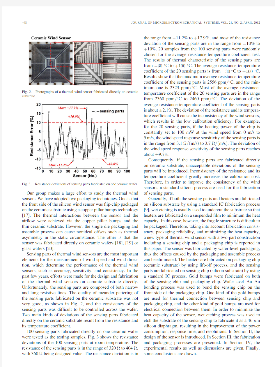
Fig.2.Photographs of a thermal wind sensor fabricated directly on ceramic
substrate.
Fig.3.Resistance deviations of sensing parts fabricated on one ceramic wafer.
Our group makes a large effort to study the thermal wind sensors.We have adopted two packaging techniques.One is that the front side of the silicon wind sensor was ?ip-chip packaged on the ceramic substrate using a copper pillar bumps technology [17].The thermal interactions between the sensor and the air?ow were achieved via the copper pillar bumps and the thin ceramic substrate.However,the single die packaging and assemble process can cause nonideal offsets such as thermal asymmetry in the static circumstance.The other is that the sensor was fabricated directly on ceramic wafers [18],[19]or glass wafers [20].
Sensing parts of thermal wind sensors are the most important elements for the measurement of wind speed and wind direc-tion,which determine the performance of the thermal wind sensors,such as accuracy,sensitivity,and consistency.In the past few years,efforts were made for the design and fabrication of the thermal wind sensors on ceramic substrate directly.Unfortunately,the sensing parts are composed of both narrow and long resistive lines.The quality of meander pattering of the sensing parts fabricated on the ceramic substrate was not very good,as shown in Fig.2,and the consistency of the sensing parts was dif?cult to be controlled across the wafer.Two main kinds of deviations of the sensing parts fabricated directly on the ceramic substrate result from the resistance and its temperature coef?cient.
100sensing parts fabricated directly on one ceramic wafer were tested as the testing samples.Fig.3shows the resistance deviations of the 100sensing parts at room temperature.The resistance of the sensing parts is in the range of 320Ωto 404Ω,with 360Ωbeing designed value.The resistance deviation is in
the range from ?11.2%to +17.9%,and most of the resistance deviation of the sensing parts are in the range from ?10%to +10%.20samples from the 100sensing parts were randomly chosen for the average resistance-temperature coef?cient test.The results of thermal characteristic of the sensing parts are from ?30?C to +100?C.The average resistance-temperature coef?cient of the 20sensing parts is from ?30?C to +100?C.Results show that the maximum average resistance-temperature coef?cient of the sensing parts is 2556ppm /?C,and the min-imum one is 2323ppm /?C.Most of the average resistance-temperature coef?cient of the 20sensing parts are in the range from 2360ppm /?C to 2460ppm /?C.The deviation of the average resistance-temperature coef?cient of the sensing parts is about ±2.1%.The deviation of the resistance and its tempera-ture coef?cient will cause the inconsistency of the wind sensors,which results in the low calibration ef?ciency.For example,for the 20sensing parts,if the heating power of the chip is constantly set to 100mW at the wind speed from 0m/s to 5m/s,the wind speed response sensitivity of the sensing parts is in the range from 3.1Ω/(m/s )to 3.7Ω/(m/s ).The deviation of the wind speed response sensitivity of the sensing parts reaches about ±9.7%.
Consequently,if the sensing parts are fabricated directly on ceramic substrate,unacceptable deviations of the sensing parts will be introduced.Inconsistency of the resistance and its temperature coef?cient greatly increases the calibration cost.Therefore,in order to improve the consistency of the wind sensors,a standard silicon process are used for the fabrication of sensing parts.
Generally,if both the sensing parts and heaters are fabricated on silicon substrate by using a standard IC fabrication process [9],wet etching is usually used to undercut the substrate so that heaters are fabricated on a suspended ?lm to minimum the heat capacity.In this case,however,the fragile structure is dif?cult to be packaged.Therefore,taking into account fabrication consis-tency,packaging reliability,and minimizing the heat capacity,a new type of thermal wind sensor with a two-part construction including a sensing chip and a packaging chip is reported in this paper.The sensor was fabricated by wafer-level packaging,thus the offsets caused by the packaging and assemble process can be eliminated.The heaters are fabricated on packaging chip (ceramic substrate)by using lift-off process,and the sensing parts are fabricated on sensing chip (silicon substrate)by using a standard IC process.Gold bumps were fabricated on both of the sensing chip and packaging chip.Wafer-level Au–Au bonding process was used to bond the sensing chip on the front side of the packaging chip.One kind of the gold bumps are used for thermal connection between sensing chip and packaging chip,and the other kind of gold bumps are used for electrical connection between them.In order to minimize the heat capacity of the sensor,wet etching process was used to etch the substrate of the sensing chip to fabricate it as a 46μm silicon diaphragm,resulting in the improvement of the power consumption,response time,and resolutions.In Section II,the design of the sensor is introduced.In Section III,the fabrication and packaging processes are presented.In Section IV,the experimental results as well as discussions are given.Finally,some conclusions are drawn.
DONG et al.:FABRICATION OF A MICROMACHINED TWO-DIMENSIONAL WIND SENSOR BY Au–Au WAFER BONDING TECHNOLOGY 469
II.S ENSOR D ESIGN
For a thermal wind ?ow sensor,the ?ow speed and direction can be measured by detecting temperature and ?ow-dependent heat distribution on its hot surface.Because the sensor to be designed measures air?ow by detecting transferred heat through the air,heat convection is the dominant factor of heat transfer.A.Power Dissipation
Heat radiation is too small to be considered when the temperature of a thermal ?ow sensor is lower than 300?C [21].The power dissipation of the sensor can be divided into P cond caused by heat conduction and P conv caused by heat convection,which is given by
P tot =P cond +P conv
(1)
where P tot is the total power dissipation of the chip.Following the boundary theory of a heated plate for a ?rst-order approxi-mation,it yields [21]
P cond ≈λL 2ΔT (2)P conv ≈hL 2ΔT
(3)
where ΔT is the overheat with respect to the air?ow,L is the chip size,λ=kc/D is the heat conduction coef?cient of the sensor,kc and D are the heat conductivity and the thickness of the ceramic substrate,respectively.The h is the convection coef?cient on the surface,which is given by [22]
h =0.664k f α?1/3ν?1/6L ?1/2U 1/2
(4)
where U ,ν,k f ,and αare the speed,the kinematic viscosity,
the heat conductivity,and the thermal diffusivity of the air?ow,respectively.Hence,P tot can be rewritten as
P tot = λL 2+0.664k f
L 3/2
α1/3ν1/6U 1/2 ΔT.(5)
It is shown that the thermal ?ow sensor obeys the King’s law in the traditional anemometer,i.e.,
P tot =(A +BU 1/2)ΔT
(6)
where A and B represent the constants depending on the chip geometry,the chip material properties,and the air?ow.B.Temperature Distribution
If a sensor chip is represented by a thin,square surface element with lateral dimensions L ×L and thickness D ,it is assumed to be thermally insulated from its substrate.There is no heat loss at the edges or the lower surface.If the value of D is much smaller than L ,the variation of the temperature across the thickness of the sensor can be omitted.When the overheat temperature is higher than the air?ow is constant (ΔT ),the value of the temperature difference (ΔT 0)between two ?xed points can be expressed as [23]
ΔT 0ΔT =c k f L k c D
(τw L 2/να)1/3G (φ)=F (U )G (φ)
(7)
Fig.4.(a)Design patterns.(b)The cross-sectional view of the fabricated sensor.(c)The left bump provides heat transfer,and the right bump provides electrical connection between the sensing chip and the packaging chip.
where c is the constant which equals to 0.08076when the temperature detectors located on the backside of the chip,τw ≈U 3/2,de?ned as the constant value of the wall shear stress τof the air?ow at the surface,G (φ)is the sensitivity function of ?ow direction,F (U )is the sensitivity function of ?ow speed,which is given by [23]
F (U )=
ΔT 0ΔT =c k f L k c D
(L 2/να)1/3√U.(8)
F (U )is proportional to L/D ,and inverse proportional to the
kc .Therefore,increasing chip size,reducing the thickness of chip and reducing lateral heat conductivity of the chip are the ways to enhance the performance of the sensor.
A 2-D direction sensitivity is obtained by measuring temper-ature difference in north-south direction (denoted as ΔT NS =ΔT 0sin Φ,corresponding to sensor output voltages V NS )and the temperature difference in east-west direction (denoted as ΔT EW =ΔT 0cos Φ,corresponding to sensor output voltages V EW ).The ?ow direction Φis independent of the ?ow speed and is determined by [23]
φ=tan ?1(V NS /V EW ).
(9)
C.Design Consideration
As shown in Fig.4,the sensor consists of a sensing chip (silicon)and a packaging chip (ceramic),in which the sensing chip is bonded to the front side of the packaging chip (ceramic)through wafer-level gold bumps.To reduce the effect of heat conduction,a silicon diaphragm is fabricated on the backside of the sensor by thinning out the silicon substrate so as to reduce its heat capacity.In addition,a silicon dioxide (SiO 2)layer,which has low heat conductivity,is formed on the silicon
470JOURNAL OF MICROELECTROMECHANICAL SYSTEMS,VOL.21,NO.2,APRIL2012
diaphragm.The heat conduction normal to the sensor may be reduced to some degree.Furthermore,the structure of the designed sensor is symmetrical,so that the heat conduction to all of the sensing parts is the same.The?ow passes over the backside of the ceramic packaging chip.The sensing chip makes thermal contact with the air?ow while still being pro-tected from direct mechanical contact.Four heaters,which are located on the backside of the ceramic plate,are used to heat the packaging chip to a constant temperature above the?ow, thus the asymmetrically cooling of?ow can induce a?ow-dependent heat distribution on its surface.The sensing chip includes ten sensing parts,two of which are located at the center and eight are located symmetrically around the center parts.The eight sensing parts form two Wheatstone full-bridges for the wind direction measurement,resulting in about50%increase of the sensitivity with respect to four sensing parts.A thermal insulation trench is located between the center pats and the others.Gold bumps are chosen here for thermal connection and electrical connection between the sensing chip and packaging chip.Three main features are considered.The?rst is that the bumps can be fabricated with different shapes and will not deform after bonded.The second is that heat transfer between the two chips can be guaranteed due to the good heat conduction properties of gold.The third is that the gold bumps can be directly fabricated on the passivation layer,which makes it pos-sible to fabricate simultaneously the thermal connection bumps (with passivation layer between the gold bumps and sensing parts)and electrical connection bumps(without passivation layer between the gold bumps and pads).
The speci?c two-part construction of the wind sensor results from the consistency of the sensing parts and the packaging reliability in batch production.Moreover,the heaters fabricated on the packaging chip will minimize the heat capacity of the sensor.Based on our previous simulation[20],all structural dimensions of the sensor have been obtained.
III.F ABRICATION AND P ACKAGING
A designed wind?ow sensor has four heaters on the pack-aging chip.A sensing chip consists of ten sensing parts on a silicon diaphragm.5μm thick gold bumps were fabricated on the packaging chip and sensing chip and then bonded together for thermal connection and electrical connection.The chip dimensions are6.0mm×6.0mm.The pattern widths of the heater and sensing parts are15μm and4μm,re-spectively.The silicon diaphragm thickness is46μm after processing.N-type,single-crystal(100)Si wafers(thickness= 400μm,diameter=100mm)were used for the fabrication of the designed sensing chip.Double-side,polished,ceramic wafers(thickness=300μm,diameter=100mm,?atness= 0.0127mm/mm,maximum surface?nish=0.0127μm.)were used for the fabrication of the designed packaging chip.
The fabrication process is shown in Fig.5.First,after clean-ing a silicon wafer,a1μm thick SiO2layer was thermally grown on the Si substrate through oxidation in order to reduce heat conduction effect.0.5μm thick aluminum was sputtered on the SiO2layer and patterned to form the thermistors as the sensing parts.Then,a passivation layer(0.1μm SiO2
+Fig.5.Fabrication process.(a)The sensing chip and the packaging chip.
(b)The wafer bonding process and TMAH etching.
0.7μm Si3N4)was made on the thermistors and patterned to form through-holes for electrical lead-out.An under bump metal(Au)was sputtered and pattered on the passivation layer, and then5μm thick gold bumps were fabricated on the silicon wafer using electroplating process,the SiO2layer acts as a blocking layer for the diffusion of the gold into the silicon substrate.Finally,dry etching process was used to remove the passivation layer,the SiO2layer,and silicon substrate so as to fabricate50μm deep trench in order to make a thermal insulation.The fabrication process of the packaging chip is as follows.3000?thick Pt was sputtered on a ceramic wafer for the fabrication of heaters.In order to improve Pt adhesion,Ti was used as an interlayer(1000?).Pt was patterned by a lift-off process.N2annealing was conducted at600?C after the lift-off process.Then,5μm thick gold bumps were fabricated on the ceramic wafer using electroplating process.The two wafers were bonded together using Au–Au bonding technology in a wafer bonding system(EVG-501)at2MPa,380?C,and30min for wafer-level packaging.The bonding area is7.4×10?4m2, and the tool force is1500N.Possible asymmetries may be introduced by the bonding.Because the sensors were fabricated by wafer-level Au–Au bonding,the asymmetries of the sensors across the wafer are the same.The asymmetries can be cali-brated simply through adjusting the heating power distribution on the chip.After the wafer-level bonding,none of defects and obviously bending of the bonded wafer has been found.Then,a silicon diaphragm was fabricated by TMAH etching at90?C to minimize heat capacity,and simultaneously resulting in the electrical feed-through in wafer-level packaging.The wet etching was performed on the backside of the bonded wafer, and a wafer holder was used to protect the rest of the structures during TMAH etching.For the protection of the sensing parts, a silicon-doped TMAH solution was adopted.
DONG et al.:FABRICATION OF A MICROMACHINED TWO-DIMENSIONAL WIND SENSOR BY Au–Au WAFER BONDING TECHNOLOGY
471
Fig.6.Photograph of the sensing chip without thermal bumps fabricated on silicon substrate by using a standard IC
process.
Fig.7.Photographs of the fabricated wind sensor,sensing chip,packaging chip,and sensor chip after processing.
Fig.6shows a photograph of the sensing chip without ther-mal bumps fabricated on silicon substrate by using a standard IC process.The photographs of a sensing chip,a packaging chip,and a fabricated wind ?ow sensor are displayed in Fig.7.The thickness of the silicon diaphragm was measured to be 46μm by using a pro?le projector (Veeko NT1100).An air gap between the sensing chip and the packaging chip is about 10μm.The resistances of the fabricated heaters,the center sensing parts,and the other sensing parts are 400Ω,100Ω,and 166Ωat room temperature,respectively.Photographs are shown in Fig.8after wet etching,dicing,and an installed ?ow sensor on a PCB in order to connect to an outer electric circuit for tests.The wind ?ow sensor made use of direct chip attachment packaging [24],[25]to achieve the
electrical
Fig.8.Photographs after wet etching,dicing,and an installed ?ow sensor on a PCB.
connection with the PCB.A metal frame was glued to the FR4substrate for protection.
After the fabrication of the two-part construction thermal wind sensor,the consistency and deviation of resistance,average resistance-temperature coef?cient,and wind speed re-sponse sensitivity have been tested.It is found that the con-sistency of the sensing parts fabricated on silicon substrate by using a standard IC process has been improved greatly.The resistance deviations of the sensing parts have been con-trolled to less than ±0.5%.Its average resistance-temperature coef?cient is about 2300ppm /?C.The deviation of average resistance temperature coef?cient is about ±0.09%.By testing in a wind tunnel at the wind speed from 0m/s to 5m/s and at 100mW heating power,the wind speed response sensitivity of the sensing parts is about 3Ω/(m/s ),and its deviation is about ±1.7%.Table I shows the comparisons of the two-part construction with one-element approach.
IV .S ENSOR S YSTEM
Fig.9shows a block diagram of a wind sensor system for measuring ?ow speed and direction.The system consists of three parts:a sensor part,a detecting part for ?ow speed and direction,and a sampling and processing part.The circuits with low-offset instrument ampli?ers,Wheatstone-bridge circuits,and OP amps are designed to amplify and modify the output signals.A microprocessor is used to control the operation of the sensor system.The output analog signal is digitalized by the analog-digital converter.
When air?ow passes over the sensor,the heating power is increased to compensate the lost heat transferred to the air?ow,so the heating power is proportional to the ?ow speed.The constant-temperature difference (CTD)control circuit is shown in Fig.10,which is used to maintain the sensor at a con-stant temperature above ambient temperature.The CTD mode ensures that the heating power has a simple square-root law relationship with ?ow speed.An off-chip ambient temperature sensor (AD590)is used to compensate the in?uence of the ambient temperature.
When air?ow encounters the hot surface of the sensor,heat transfer from the surface to the air?ow is largest at the up-stream side.The upstream temperature will become slightly lower and the downstream temperature slightly higher than the average temperature of the chip.A small temperature
472JOURNAL OF MICROELECTROMECHANICAL SYSTEMS,VOL.21,NO.2,APRIL 2012
TABLE I
C OMPARISONS OF C ONSISTENCY AN
D D EVIATIONS OF S ENSING P ARTS F ABRICATED ON C ERAMIC W AFER AND S ILICON W
AFER
Fig.9.Block diagram of the wind ?ow sensor
system.
Fig.10.Constant-temperature difference control circuit for power control and ?ow speed detection.
gradient (ΔT NS and ΔT EW )over the sensor is induced due to this nonuniform cooling effect.The temperature difference can be measured by detecting the eight sensing parts formed as two Wheatstone-bridge circuits.The temperature difference increases with the ?ow speed,and it is also sensitive to the ?ow direction.In calorimetric system,two instrument ampli?ers are used to amplify the output voltages (ΔV NS and ΔV EW )of two Wheatstone-bridges,which have a linear law relationship with the two orthogonal comments (ΔT NS and ΔT EW )of the ?ow-induced temperature gradient.According to (9),the ampli?ed voltage V NS and V EW can be used to calculate the
?ow direction.Moreover,the V 2NS
+V 2
EW has a square law relationship with ?ow speed.
V .R ESULTS AND D ISCUSSION
As shown in Fig.11,a fabricated sensor was installed in a laminar ?ow wind-tunnel covering ?ow velocity up to 40m/s and a full range of 360?for ?ow direction measurements.
At
Fig.11.
Experimental setup and the wind
tunnel.
Fig.12.Temperature characteristic of sensing parts on a silicon chip at the ambient temperature ranging from ?30?C to +60?C.
the location of the sensor,the cross-section area of the wind-tunnel is 25×25cm 2.The ?ow velocity was measured using a pitot tube,with accuracy better than 1.0%of the full scale in the range from 0.5to 40m/s.The temperature characteristics of sensing parts fabricated on a sensing chip are shown in Fig.12.The R detectors NSEW are located on the sensing chip around the R detectors C,and R detectors C are located in the center of the sensing chip.R detectors NSEW are used to detect the temperature difference between the upstream and downstream,and R detectors C are used to detect the center temperature of the chip.
Their temperature coef?cients are linear at the ambient tem-perature ranging from ?30?C to +60?C,which is about
DONG et al.:FABRICATION OF A MICROMACHINED TWO-DIMENSIONAL WIND SENSOR BY Au–Au WAFER BONDING TECHNOLOGY
473
Fig.13.(a)Flow speed as a function of heating power at different overheat temperature in CTD mode.(b)Relationship of the heating power with the square root of?ow speed.ΔT is the overheat temperature and P0is the initial heating power.
2300ppm.The consistency of the temperature characteristics of these sensing parts indicates that the bonded gold bumps can ensure good thermal connection and electrical connection between the two chips.Therefore,Au–Au bonding technology may be considered as a promising method for electrical con-nections and thermal connections in the wafer-level packaging of the thermal?ow sensors.Fig.13shows the heating power as a function of?ow speed.Results show that the heating power keeps a linear relationship with the square root of?ow speed. The measurement of the?ow speed ranging from0.5to40m/s has an accuracy of±4%after calibration by using a look-up table.
When the overheat temperature is ranging from6?C to 45?C,the initial heating power will be ranging from2mW to85mW.With2mW initial heating power(overheat temperature=6?C),the sensor sensitivity for?ow speed in the CTD mode is better than2.73mW/ms?1for the full testing range.When the overheat temperature is ranging from6?C to45?C,the heating power is ranging from111.2mW to 452.6mW at the?ow speed of40m/s.The sensitivity can reach9mW/ms?1when the initial heating power is set to be 85mW.Fig.14shows the output voltage(the root of V2NS+ V2EW)of the calorimetric system,which operates in the CP (100mW constant heating power)and CTD(2mW initial heating power)mode,respectively,as a function of?ow
speed.Fig.14.Flow speed characteristic of calorimetric system operating in CP and CTD
modes.
Fig.15.Sensor response for?ow speed from5to10m/s and from10 to5m/s.
The output sensitivity in the CP mode is larger than that in the CTD mode at the?ow speed up to19.5m/s,while the output signals in the CP mode tend to saturate when the?ow speed is higher than20m/s.In the CTD mode,the output voltages keep the sensitivity(7.85mV/ms?1)for the?ow speed ranging from0.5to40m/s.Therefore,it is considered as a promising mode for?ow direction measurement in high?ow speed circumstances.
By detecting the output voltages of an ampli?er used to amplify the heating voltages,the sensor response to?ow speed change can be measured when an abrupt change of the?ow speed occurs.As shown in Fig.15,the response time is de?ned here as the90%value of the time cost for the change of the output voltages.It shows that the response time is less than1.4s and1.2s from5m/s to10m/s and10m/s to5m/s,respectively. The raw output voltages of the calorimetric system at different ?ow speeds are shown in Fig.16.The output voltages of the calorimetric system are very close to the cosine(sine)function of?ow direction.The measurement of?ow direction in a full range of360?has an accuracy of±2?over the full range of?ow speed.
VI.C ONCLUSION
A micromachined2-D thermal wind?ow sensor by wafer-level packaging through Au–Au bonding technology has been
474JOURNAL OF MICROELECTROMECHANICAL SYSTEMS,VOL.21,NO.2,APRIL
2012
Fig.16.Output voltages of calorimetric system for?ow direction measure-ment at different?ow speeds.
presented,fabricated,and tested.Gold bumps were used for thermal connection and electrical connection.The wafer-level packaging process reduces the offsets caused by the separate packaging and assembly.A silicon diaphragm was fabricated by wet etching,resulting in the improvement of the power consumption,response time,and resolutions.The measured ?ow speed reaches40m/s with only2mW initial heating power in CTD mode.The?ow direction in a full range of360?may be measured.The errors in the measured?ow speed and direction are±4%and±2?after calibration,https://www.360docs.net/doc/c614093550.html,pared with other MEMS-based wind sensor,the present sensor can measure?ow speed as high as40m/s with low heating power.
R EFERENCES
[1]A.F.P.Van Putten and S.Middlehoek,“Integrated silicon anemometer,”
Electron.Lett.,vol.10,no.21,pp.425–426,Oct.1974.
[2]B.W.van Oudheusden,“Silicon thermal?ow sensors,”Sens.Actuators
A,Phys.,vol.30,no.1/2,pp.5–26,Jan.1992.
[3]N.T.Nguyen,“Micromachined?ow sensors—A review,”Flow Meas.
Instrum.,vol.8,pp.7–16,Mar.1997.
[4]M.Mischler,F.-G.Tseng,U.Ulmanella,C.-M.Ho,F.Jiang,and Y.-C.Tai,
“A micro silicon hot-wire anemometer,”in Proc.IEEE TENCON,Hong Kong,1995,pp.20–23.
[5]M.Elwenspoek,“Thermal?ow micro sensors,”in Proc.Semicond.Conf.,
Sinaia,Romania,1999,pp.423–435.
[6]S.K.Gamage,N.Okulan,and H.T.Henderson,“Behavior of bulk
micromachined silicon?ow sensor in the negative differential resistance regime,”J.Micromech.Microeng.,vol.10,no.3,pp.421–429,Sep.2000.
[7]H.Baltes,O.Paul,and O.Brand,“Micromachined thermally based
CMOS microsensors,”Proc.IEEE,vol.86,no.8,pp.1660–1678, Aug.1998.
[8]S.Hung,S.Wong,and W.Fang,“The development and application of
microthermal sensors with a mesh-membrane supporting structure,”Sens.
Actuators A,Phys.,vol.84,no.1/2,pp.70–75,Aug.2000.
[9]S.Kim,S.Kim,Y.Kim,and S.Park,“A circular-type thermal?ow
direction sensor free from temperature compensation,”Sens.Actuators A,Phys.,vol.108,no.1–3,pp.64–68,Nov.2003.
[10]N.Sabaté,J.Santander,L.Fonseca,I.Gràcia,and C.Cané,“Multi-range
silicon micromachined?ow sensor,”Sens.Actuators A,Phys.,vol.110, no.1–3,pp.282–288,Feb.2004.
[11]J.Chen and C.Liu,“Development and characterization of surface mi-
cromachined,out-of-plane hot-wire anemometer,”J.Microelectromech.
Syst.,vol.12,no.6,pp.979–988,Dec.2003.
[12]K.A.A.Makinwa and J.H.Huijsing,“A smart CMOS wind sensor,”in
Proc.IEEE ISSCC.,San Francisco,CA,2002,pp.432–479.
[13]K.A.A.Makinwa,J.H.Huijsing,and A.Hagedoorn,“A solid-state2-D
wind sensor,”in Proc.SAMOS,vol.4017,Lecture Notes in Computer Science,Jul.2006,pp.477–484.[14]J.Wu,Y.Chae,C.P.L.van Vroonhoven,and K.A.A.Makinwa,“A
50mW CMOS wind sensor with±4%speed and±2?direction error,”in Proc.IEEE ISSCC,San Francisco,CA,2011,pp.106–108.
[15]S.P.Matova,K.A.A.Makinwa,and J.H.Huijsing,“Compensation of
packaging asymmetry in a2-D wind sensor,”IEEE Sensors J.,vol.3, no.6,pp.761–765,Dec.2003.
[16]F.Mayer,O.Paul,and H.Baltes,“Flip-chip packaging for thermal CMOS
anemometers,”in Proc.10th IEEE Int.Conf.MEMS,Nagoya,Japan, 1997,pp.203–208.
[17]J.B.Sun,M.Qin,and Q.A.Huang,“Flip-chip packaging for a two-
dimensional thermal?ow sensor using a copper pillar bump technology,”
IEEE Sensors J.,vol.7,no.7,pp.990–995,Jul.2007.
[18]Z.Dong,Q.A.Huang,and M.Qin,“Thermal asymmetry compensation
of a wind sensor fabricated on ceramic substrate,”in Proc.9th IEEE Conf.
Sensors,Waikoloa,HI,2010,pp.595–599.
[19]G.P.Shen,M.Qin,Z.Dong,and Q.A.Huang,“An intelligent wind sensor
system with auto-zero function,”in Proc.15th Int.Conf.Solid-State Sens., Actuators,Microsyst.(TRANSDUCERS),Denver,CO,2009,pp.256–259.
[20]G.P.Shen,M.Qin,and Q.A.Huang,“A cross-type thermal wind sensor
with self-testing function,”IEEE Sensors J.,vol.10,no.2,pp.340–346, Feb.2010.
[21]J.P.Holman,Heat Transfer.New York:McGraw-Hill,2007,pp.49–
202.
[22]Z.Rotem,“The effect of thermal conduction of the wall upon convection
from a surface in a laminar boundary layer,”Int.J.Heat Mass Transf., vol.10,no.4,pp.461–466,Apr.1967.
[23]B.W.Van Oudheusden,“Silicon thermal?ow sensor with a two-
dimensional direction sensitivity,”Meas.Sci.Technol.,vol.1,no.7, pp.565–575,Jul.1990.
[24]D.R.Gamota and C.M.Melton,“The development of re?owable ma-
terials systems to integrate the re?ow and under?ll dispensing processes for DCA/FCOB assembly,”IEEE https://www.360docs.net/doc/c614093550.html,put.,vol.20,no.3,pp.183–187,Jul.1997.
[25]G.P.Shen,J.Wu,H.Zhang,M.Qin,and Q.A.Huang,“Direct chip
attachment(DCA)packaging of a2-D thermal?ow sensor,”in Proc.IEEE ICEPT,Shanghai,China,2007,pp.
1–3.
Ziqiang Dong was born in Hebei,China,in1982.
He received the B.S.and M.S.degrees in elec-
tronic engineering from Hebei University of Sci-
ence and Technology,Hebei,China,in2004and
2007,respectively.He is currently working toward
the Ph.D.degree at Southeast University,Nanjing,
China.
His current research focuses on the design,fabri-
cation,and test of wind/?ow
sensors.
Jingjing Chen was born in1988.She received the
B.S.degree in electronic engineering from Anhui
University,Hefei,China,in2009.She is currently
working toward the M.S.degree in the Key Lab-
oratory of MEMS of the Ministry of Education,
Southeast University,Nanjing,China.
Her main research interests are in the design and
simulation of MEMS
sensors.
Yukun Qin was born in1987.He received the B.S.
degree in electronic engineering from Anhui Univer-
sity,Hefei,China,in2009.He is currently work-
ing toward the M.S.degree in the Key Laboratory
of MEMS of the Ministry of Education,Southeast
University,Nanjing,China.
His main research interests is signal processing of
MEMS sensors.
DONG et al.:FABRICATION OF A MICROMACHINED TWO-DIMENSIONAL WIND SENSOR BY Au–Au WAFER BONDING TECHNOLOGY
475
Ming Qin(M’07)was born in China in1967.He
received the B.S.degree in electrical engineering
from Wuxi Institute of Technology,Jiangsu,China,
in1988,and the M.S.and Ph.D.degrees in electri-
cal engineering from Southeast University,Nanjing,
China,in1994and1997,respectively.
After graduation,he became an Assistant Profes-
sor in the Department of Electronic Engineering,
Southeast University,where he became an Associate
Professor in1999and a Full Professor in2003.
He was a Postdoctoral Researcher at Hong Kong University of Science and Technology in1999.He has served as Director of the CMOS MEMS Branch of the Key Laboratory of MEMS of the Ministry of Education in China.He has published over30peer-reviewed international journal/conference papers and holds more than20Chinese
patents.
Qing-An Huang(S’89–M’91–SM’95)received the
B.S.degree in electronic engineering from Hefei
University of Technology,Hefei,China,in1983,the
M.S.degree in electronic engineering from Xidian
University,Xi’an,China,in1987,and the Ph.D.
degree in electronic engineering from Southeast Uni-
versity,Nanjing,China,in1991.His Ph.D.research
focused on micromachined GaAs piezoelectric
sensors.
After graduation,he joined the faculty of the De-
partment of Electronic Engineering,Southeast Uni-versity,as an Assistant Professor,where he became an Associate Professor in 1993,a Full Professor in1996,and was specially appointed to Professor for the Chang-Jiang Scholar by the Ministry of Education in2004.He was a Visiting Scholar at Hong Kong University of Science and Technology,Hong Kong,from 1997to1998.He is currently the founding Director of the Key Laboratory of MEMS of the Ministry of Education,Southeast University.He has authored a book entitled Silicon Micromachining Technology(Science Press,1996),and published over100peer-reviewed international journals/conference papers.He is the holder of30Chinese patents.
Dr.Huang has served as Editor-in-Chief of the Chinese Journal of Sensors and Actuators.He was a Conference Cochair for the SPIE-Microfabrication and Micromachining Process Technology and Devices(Conference Proc. SPIE,vol.4601,November2001),Technical Program Cochair for the 7th IEEE International Conference on NEMS,and a TPC Member of TRANSDUCERS’09&’11as well as the IEEE Sensors Conference through 2002to2010.He has served as a Steering Committee Member of The Asia-Paci?c Conference of Transducers and Micro/Nano Technology(APCOT) (2008–2012).He served as the founding Chairman of the IEEE ED/SSC Joint Chapter(Nanjing).He received the National Outstanding Youth Science Foundation Award of China in2003.
从实践的角度探讨在日语教学中多媒体课件的应用
从实践的角度探讨在日语教学中多媒体课件的应用 在今天中国的许多大学,为适应现代化,信息化的要求,建立了设备完善的适应多媒体教学的教室。许多学科的研究者及现场教员也积极致力于多媒体软件的开发和利用。在大学日语专业的教学工作中,教科书、磁带、粉笔为主流的传统教学方式差不多悄然向先进的教学手段而进展。 一、多媒体课件和精品课程的进展现状 然而,目前在专业日语教学中能够利用的教学软件并不多见。比如在中国大学日语的专业、第二外語用教科书常见的有《新编日语》(上海外语教育出版社)、《中日交流标准日本語》(初级、中级)(人民教育出版社)、《新编基础日语(初級、高級)》(上海译文出版社)、《大学日本语》(四川大学出版社)、《初级日语》《中级日语》(北京大学出版社)、《新世纪大学日语》(外语教学与研究出版社)、《综合日语》(北京大学出版社)、《新编日语教程》(华东理工大学出版社)《新编初级(中级)日本语》(吉林教育出版社)、《新大学日本语》(大连理工大学出版社)、《新大学日语》(高等教育出版社)、《现代日本语》(上海外语教育出版社)、《基础日语》(复旦大学出版社)等等。配套教材以录音磁带、教学参考、习题集为主。只有《中日交流標準日本語(初級上)》、《初級日语》、《新编日语教程》等少数教科书配备了多媒体DVD视听教材。 然而这些试听教材,有的内容为日语普及读物,并不适合专业外语课堂教学。比如《新版中日交流标准日本语(初级上)》,有的尽管DVD视听教材中有丰富的动画画面和语音练习。然而,课堂操作则花费时刻长,不利于教师重点指导,更加适合学生的课余练习。比如北京大学的《初级日语》等。在这种情形下,许多大学的日语专业致力于教材的自主开发。 其中,有些大学的还推出精品课程,取得了专门大成绩。比如天津外国语学院的《新编日语》多媒体精品课程为2007年被评为“国家级精品课”。目前已被南开大学外国语学院、成都理工大学日语系等全国40余所大学推广使用。
新视野大学英语全部课文原文
Unit1 Americans believe no one stands still. If you are not moving ahead, you are falling behind. This attitude results in a nation of people committed to researching, experimenting and exploring. Time is one of the two elements that Americans save carefully, the other being labor. "We are slaves to nothing but the clock,” it has been said. Time is treated as if it were something almost real. We budget it, save it, waste it, steal it, kill it, cut it, account for it; we also charge for it. It is a precious resource. Many people have a rather acute sense of the shortness of each lifetime. Once the sands have run out of a person’s hourglass, they cannot be replaced. We want every minute to count. A foreigner’s first impression of the U.S. is li kely to be that everyone is in a rush -- often under pressure. City people always appear to be hurrying to get where they are going, restlessly seeking attention in a store, or elbowing others as they try to complete their shopping. Racing through daytime meals is part of the pace
新视野大学英语第三版第二册课文语法讲解 Unit4
新视野三版读写B2U4Text A College sweethearts 1I smile at my two lovely daughters and they seem so much more mature than we,their parents,when we were college sweethearts.Linda,who's21,had a boyfriend in her freshman year she thought she would marry,but they're not together anymore.Melissa,who's19,hasn't had a steady boyfriend yet.My daughters wonder when they will meet"The One",their great love.They think their father and I had a classic fairy-tale romance heading for marriage from the outset.Perhaps,they're right but it didn't seem so at the time.In a way, love just happens when you least expect it.Who would have thought that Butch and I would end up getting married to each other?He became my boyfriend because of my shallow agenda:I wanted a cute boyfriend! 2We met through my college roommate at the university cafeteria.That fateful night,I was merely curious,but for him I think it was love at first sight."You have beautiful eyes",he said as he gazed at my face.He kept staring at me all night long.I really wasn't that interested for two reasons.First,he looked like he was a really wild boy,maybe even dangerous.Second,although he was very cute,he seemed a little weird. 3Riding on his bicycle,he'd ride past my dorm as if"by accident"and pretend to be surprised to see me.I liked the attention but was cautious about his wild,dynamic personality.He had a charming way with words which would charm any girl.Fear came over me when I started to fall in love.His exciting"bad boy image"was just too tempting to resist.What was it that attracted me?I always had an excellent reputation.My concentration was solely on my studies to get superior grades.But for what?College is supposed to be a time of great learning and also some fun.I had nearly achieved a great education,and graduation was just one semester away.But I hadn't had any fun;my life was stale with no component of fun!I needed a boyfriend.Not just any boyfriend.He had to be cute.My goal that semester became: Be ambitious and grab the cutest boyfriend I can find. 4I worried what he'd think of me.True,we lived in a time when a dramatic shift in sexual attitudes was taking place,but I was a traditional girl who wasn't ready for the new ways that seemed common on campus.Butch looked superb!I was not immune to his personality,but I was scared.The night when he announced to the world that I was his girlfriend,I went along
新视野大学英语读写教程第一册课文翻译及课后答案
Unit 1 1学习外语是我一生中最艰苦也是最有意义的经历之一。虽然时常遭遇挫折,但却非常有价值。 2我学外语的经历始于初中的第一堂英语课。老师很慈祥耐心,时常表扬学生。由于这种积极的教学方法,我踊跃回答各种问题,从不怕答错。两年中,我的成绩一直名列前茅。 3到了高中后,我渴望继续学习英语。然而,高中时的经历与以前大不相同。以前,老师对所有的学生都很耐心,而新老师则总是惩罚答错的学生。每当有谁回答错了,她就会用长教鞭指着我们,上下挥舞大喊:“错!错!错!”没有多久,我便不再渴望回答问题了。我不仅失去了回答问题的乐趣,而且根本就不想再用英语说半个字。 4好在这种情况没持续多久。到了大学,我了解到所有学生必须上英语课。与高中老师不。大学英语老师非常耐心和蔼,而且从来不带教鞭!不过情况却远不尽如人意。由于班大,每堂课能轮到我回答的问题寥寥无几。上了几周课后,我还发现许多同学的英语说得比我要好得多。我开始产生一种畏惧感。虽然原因与高中时不同,但我却又一次不敢开口了。看来我的英语水平要永远停步不前了。 5直到几年后我有机会参加远程英语课程,情况才有所改善。这种课程的媒介是一台电脑、一条电话线和一个调制解调器。我很快配齐了必要的设备并跟一个朋友学会了电脑操作技术,于是我每周用5到7天在网上的虚拟课堂里学习英语。 6网上学习并不比普通的课堂学习容易。它需要花许多的时间,需要学习者专心自律,以跟上课程进度。我尽力达到课程的最低要求,并按时完成作业。 7我随时随地都在学习。不管去哪里,我都随身携带一本袖珍字典和笔记本,笔记本上记着我遇到的生词。我学习中出过许多错,有时是令人尴尬的错误。有时我会因挫折而哭泣,有时甚至想放弃。但我从未因别的同学英语说得比我快而感到畏惧,因为在电脑屏幕上作出回答之前,我可以根据自己的需要花时间去琢磨自己的想法。突然有一天我发现自己什么都懂了,更重要的是,我说起英语来灵活自如。尽管我还是常常出错,还有很多东西要学,但我已尝到了刻苦学习的甜头。 8学习外语对我来说是非常艰辛的经历,但它又无比珍贵。它不仅使我懂得了艰苦努力的意义,而且让我了解了不同的文化,让我以一种全新的思维去看待事物。学习一门外语最令人兴奋的收获是我能与更多的人交流。与人交谈是我最喜欢的一项活动,新的语言使我能与陌生人交往,参与他们的谈话,并建立新的难以忘怀的友谊。由于我已能说英语,别人讲英语时我不再茫然不解了。我能够参与其中,并结交朋友。我能与人交流,并能够弥合我所说的语言和所处的文化与他们的语言和文化之间的鸿沟。 III. 1. rewarding 2. communicate 3. access 4. embarrassing 5. positive 6. commitment 7. virtual 8. benefits 9. minimum 10. opportunities IV. 1. up 2. into 3. from 4. with 5. to 6. up 7. of 8. in 9. for 10.with V. 1.G 2.B 3.E 4.I 5.H 6.K 7.M 8.O 9.F 10.C Sentence Structure VI. 1. Universities in the east are better equipped, while those in the west are relatively poor. 2. Allan Clark kept talking the price up, while Wilkinson kept knocking it down. 3. The husband spent all his money drinking, while his wife saved all hers for the family. 4. Some guests spoke pleasantly and behaved politely, while others wee insulting and impolite. 5. Outwardly Sara was friendly towards all those concerned, while inwardly she was angry. VII. 1. Not only did Mr. Smith learn the Chinese language, but he also bridged the gap between his culture and ours. 2. Not only did we learn the technology through the online course, but we also learned to communicate with friends in English. 3. Not only did we lose all our money, but we also came close to losing our lives.
新大学日语简明教程课文翻译
新大学日语简明教程课文翻译 第21课 一、我的留学生活 我从去年12月开始学习日语。已经3个月了。每天大约学30个新单词。每天学15个左右的新汉字,但总记不住。假名已经基本记住了。 简单的会话还可以,但较难的还说不了。还不能用日语发表自己的意见。既不能很好地回答老师的提问,也看不懂日语的文章。短小、简单的信写得了,但长的信写不了。 来日本不久就迎来了新年。新年时,日本的少女们穿着美丽的和服,看上去就像新娘。非常冷的时候,还是有女孩子穿着裙子和袜子走在大街上。 我在日本的第一个新年过得很愉快,因此很开心。 现在学习忙,没什么时间玩,但周末常常运动,或骑车去公园玩。有时也邀朋友一起去。虽然我有国际驾照,但没钱,买不起车。没办法,需要的时候就向朋友借车。有几个朋友愿意借车给我。 二、一个房间变成三个 从前一直认为睡在褥子上的是日本人,美国人都睡床铺,可是听说近来纽约等大都市的年轻人不睡床铺,而是睡在褥子上,是不是突然讨厌起床铺了? 日本人自古以来就睡在褥子上,那自有它的原因。人们都说日本人的房子小,从前,很少有人在自己的房间,一家人住在一个小房间里是常有的是,今天仍然有人过着这样的生活。 在仅有的一个房间哩,如果要摆下全家人的床铺,就不能在那里吃饭了。这一点,褥子很方便。早晨,不需要褥子的时候,可以收起来。在没有了褥子的房间放上桌子,当作饭厅吃早饭。来客人的话,就在那里喝茶;孩子放学回到家里,那房间就成了书房。而后,傍晚又成为饭厅。然后收起桌子,铺上褥子,又成为了全家人睡觉的地方。 如果是床铺的话,除了睡觉的房间,还需要吃饭的房间和书房等,但如果使用褥子,一个房间就可以有各种用途。 据说从前,在纽约等大都市的大学学习的学生也租得起很大的房间。但现在房租太贵,租不起了。只能住更便宜、更小的房间。因此,似乎开始使用睡觉时作床,白天折小能成为椅子的、方便的褥子。
新视野大学英语第一册Unit 1课文翻译
新视野大学英语第一册Unit 1课文翻译 学习外语是我一生中最艰苦也是最有意义的经历之一。 虽然时常遭遇挫折,但却非常有价值。 我学外语的经历始于初中的第一堂英语课。 老师很慈祥耐心,时常表扬学生。 由于这种积极的教学方法,我踊跃回答各种问题,从不怕答错。 两年中,我的成绩一直名列前茅。 到了高中后,我渴望继续学习英语。然而,高中时的经历与以前大不相同。 以前,老师对所有的学生都很耐心,而新老师则总是惩罚答错的学生。 每当有谁回答错了,她就会用长教鞭指着我们,上下挥舞大喊:“错!错!错!” 没有多久,我便不再渴望回答问题了。 我不仅失去了回答问题的乐趣,而且根本就不想再用英语说半个字。 好在这种情况没持续多久。 到了大学,我了解到所有学生必须上英语课。 与高中老师不同,大学英语老师非常耐心和蔼,而且从来不带教鞭! 不过情况却远不尽如人意。 由于班大,每堂课能轮到我回答的问题寥寥无几。 上了几周课后,我还发现许多同学的英语说得比我要好得多。 我开始产生一种畏惧感。 虽然原因与高中时不同,但我却又一次不敢开口了。 看来我的英语水平要永远停步不前了。 直到几年后我有机会参加远程英语课程,情况才有所改善。 这种课程的媒介是一台电脑、一条电话线和一个调制解调器。 我很快配齐了必要的设备并跟一个朋友学会了电脑操作技术,于是我每周用5到7天在网上的虚拟课堂里学习英语。 网上学习并不比普通的课堂学习容易。 它需要花许多的时间,需要学习者专心自律,以跟上课程进度。 我尽力达到课程的最低要求,并按时完成作业。 我随时随地都在学习。 不管去哪里,我都随身携带一本袖珍字典和笔记本,笔记本上记着我遇到的生词。 我学习中出过许多错,有时是令人尴尬的错误。 有时我会因挫折而哭泣,有时甚至想放弃。 但我从未因别的同学英语说得比我快而感到畏惧,因为在电脑屏幕上作出回答之前,我可以根据自己的需要花时间去琢磨自己的想法。 突然有一天我发现自己什么都懂了,更重要的是,我说起英语来灵活自如。 尽管我还是常常出错,还有很多东西要学,但我已尝到了刻苦学习的甜头。 学习外语对我来说是非常艰辛的经历,但它又无比珍贵。 它不仅使我懂得了艰苦努力的意义,而且让我了解了不同的文化,让我以一种全新的思维去看待事物。 学习一门外语最令人兴奋的收获是我能与更多的人交流。 与人交谈是我最喜欢的一项活动,新的语言使我能与陌生人交往,参与他们的谈话,并建立新的难以忘怀的友谊。 由于我已能说英语,别人讲英语时我不再茫然不解了。 我能够参与其中,并结交朋友。
新大学日语阅读与写作1 第3课译文
习惯与礼仪 我是个漫画家,对旁人细微的动作、不起眼的举止等抱有好奇。所以,我在国外只要做错一点什么,立刻会比旁人更为敏锐地感觉到那个国家的人们对此作出的反应。 譬如我多次看到过,欧美人和中国人见到我们日本人吸溜吸溜地出声喝汤而面露厌恶之色。过去,日本人坐在塌塌米上,在一张低矮的食案上用餐,餐具离嘴较远。所以,养成了把碗端至嘴边吸食的习惯。喝羹匙里的东西也象吸似的,声声作响。这并非哪一方文化高或低,只是各国的习惯、礼仪不同而已。 日本人坐在椅子上围桌用餐是1960年之后的事情。当时,还没有礼仪规矩,甚至有人盘着腿吃饭。外国人看见此景大概会一脸厌恶吧。 韩国女性就座时,单腿翘起。我认为这种姿势很美,但习惯于双膝跪坐的日本女性大概不以为然,而韩国女性恐怕也不认为跪坐为好。 日本等多数亚洲国家,常有人习惯在路上蹲着。欧美人会联想起狗排便的姿势而一脸厌恶。 日本人常常把手放在小孩的头上说“好可爱啊!”,而大部分外国人会不愿意。 如果向回教国家的人们劝食猪肉和酒,或用左手握手、递东西,会不受欢迎的。当然,饭菜也用右手抓着吃。只有从公用大盘往自己的小盘里分食用的公勺是用左手拿。一旦搞错,用黏糊糊的右手去拿,
会遭人厌恶。 在欧美,对不受欢迎的客人不说“请脱下外套”,所以电视剧中的侦探哥隆波总是穿着外套。访问日本家庭时,要在门厅外脱掉外套后进屋。穿到屋里会不受欢迎的。 这些习惯只要了解就不会出问题,如果因为不知道而遭厌恶、憎恨,实在心里难受。 过去,我曾用色彩图画和简短的文字画了一本《关键时刻的礼仪》(新潮文库)。如今越发希望用各国语言翻译这本书。以便能对在日本的外国人有所帮助。同时希望有朝一日以漫画的形式画一本“世界各国的习惯与礼仪”。 练习答案 5、 (1)止める並んでいる見ているなる着色した (2)拾った入っていた行ったしまった始まっていた
新视野大学英语(第三版)读写教程第二册课文翻译(全册)
新视野大学英语第三版第二册读写课文翻译 Unit 1 Text A 一堂难忘的英语课 1 如果我是唯一一个还在纠正小孩英语的家长,那么我儿子也许是对的。对他而言,我是一个乏味的怪物:一个他不得不听其教诲的父亲,一个还沉湎于语法规则的人,对此我儿子似乎颇为反感。 2 我觉得我是在最近偶遇我以前的一位学生时,才开始对这个问题认真起来的。这个学生刚从欧洲旅游回来。我满怀着诚挚期待问她:“欧洲之行如何?” 3 她点了三四下头,绞尽脑汁,苦苦寻找恰当的词语,然后惊呼:“真是,哇!” 4 没了。所有希腊文明和罗马建筑的辉煌居然囊括于一个浓缩的、不完整的语句之中!我的学生以“哇!”来表示她的惊叹,我只能以摇头表达比之更强烈的忧虑。 5 关于正确使用英语能力下降的问题,有许多不同的故事。学生的确本应该能够区分诸如their/there/they're之间的不同,或区别complimentary 跟complementary之间显而易见的差异。由于这些知识缺陷,他们承受着大部分不该承受的批评和指责,因为舆论认为他们应该学得更好。 6 学生并不笨,他们只是被周围所看到和听到的语言误导了。举例来说,杂货店的指示牌会把他们引向stationary(静止处),虽然便笺本、相册、和笔记本等真正的stationery(文具用品)并没有被钉在那儿。朋友和亲人常宣称They've just ate。实际上,他们应该说They've just eaten。因此,批评学生不合乎情理。 7 对这种缺乏语言功底而引起的负面指责应归咎于我们的学校。学校应对英语熟练程度制定出更高的标准。可相反,学校只教零星的语法,高级词汇更是少之又少。还有就是,学校的年轻教师显然缺乏这些重要的语言结构方面的知识,因为他们过去也没接触过。学校有责任教会年轻人进行有效的语言沟通,可他们并没把语言的基本框架——准确的语法和恰当的词汇——充分地传授给学生。
新视野大学英语1课文翻译
新视野大学英语1课文翻译 1下午好!作为校长,我非常自豪地欢迎你们来到这所大学。你们所取得的成就是你们自己多年努力的结果,也是你们的父母和老师们多年努力的结果。在这所大学里,我们承诺将使你们学有所成。 2在欢迎你们到来的这一刻,我想起自己高中毕业时的情景,还有妈妈为我和爸爸拍的合影。妈妈吩咐我们:“姿势自然点。”“等一等,”爸爸说,“把我递给他闹钟的情景拍下来。”在大学期间,那个闹钟每天早晨叫醒我。至今它还放在我办公室的桌子上。 3让我来告诉你们一些你们未必预料得到的事情。你们将会怀念以前的生活习惯,怀念父母曾经提醒你们要刻苦学习、取得佳绩。你们可能因为高中生活终于结束而喜极而泣,你们的父母也可能因为终于不用再给你们洗衣服而喜极而泣!但是要记住:未来是建立在过去扎实的基础上的。 4对你们而言,接下来的四年将会是无与伦比的一段时光。在这里,你们拥有丰富的资源:有来自全国各地的有趣的学生,有学识渊博又充满爱心的老师,有综合性图书馆,有完备的运动设施,还有针对不同兴趣的学生社团——从文科社团到理科社团、到社区服务等等。你们将自由地探索、学习新科目。你们要学着习惯点灯熬油,学着结交充满魅力的人,学着去追求新的爱好。我想鼓励你们充分利用这一特殊的经历,并用你们的干劲和热情去收获这一机会所带来的丰硕成果。 5有这么多课程可供选择,你可能会不知所措。你不可能选修所有的课程,但是要尽可能体验更多的课程!大学里有很多事情可做可学,每件事情都会为你提供不同视角来审视世界。如果我只能给你们一条选课建议的话,那就是:挑战自己!不要认为你早就了解自己对什么样的领域最感兴趣。选择一些你从未接触过的领域的课程。这样,你不仅会变得更加博学,而且更有可能发现一个你未曾想到的、能成就你未来的爱好。一个绝佳的例子就是时装设计师王薇薇,她最初学的是艺术史。随着时间的推移,王薇薇把艺术史研究和对时装的热爱结合起来,并将其转化为对设计的热情,从而使她成为全球闻名的设计师。 6在大学里,一下子拥有这么多新鲜体验可能不会总是令人愉快的。在你的宿舍楼里,住在你隔壁寝室的同学可能会反复播放同一首歌,令你头痛欲裂!你可能喜欢早起,而你的室友却是个夜猫子!尽管如此,你和你的室友仍然可能成
新视野大学英语2课文翻译
新视野大学英语2课文翻译(Unit1-Unit7) Unit 1 Section A 时间观念强的美国人 Para. 1 美国人认为没有人能停止不前。如果你不求进取,你就会落伍。这种态度造就了一个投身于研究、实验和探索的民族。时间是美国人注意节约的两个要素之一,另一个是劳力。 Para. 2 人们一直说:“只有时间才能支配我们。”人们似乎是把时间当作一个差不多是实实在在的东西来对待的。我们安排时间、节约时间、浪费时间、挤抢时间、消磨时间、缩减时间、对时间的利用作出解释;我们还要因付出时间而收取费用。时间是一种宝贵的资源,许多人都深感人生的短暂。时光一去不复返。我们应当让每一分钟都过得有意义。 Para. 3 外国人对美国的第一印象很可能是:每个人都匆匆忙忙——常常处于压力之下。城里人看上去总是在匆匆地赶往他们要去的地方,在商店里他们焦躁不安地指望店员能马上来为他们服务,或者为了赶快买完东西,用肘来推搡他人。白天吃饭时人们也都匆匆忙忙,这部分地反映出这个国家的生活节奏。工作时间被认为是宝贵的。Para. 3b 在公共用餐场所,人们都等着别人吃完后用餐,以便按时赶回去工作。你还会发现司机开车很鲁莽,人们推搡着在你身边过去。你会怀念微笑、简短的交谈以及与陌生人的随意闲聊。不要觉得这是针对你个人的,这是因为人们非常珍惜时间,而且也不喜欢他人“浪费”时间到不恰当的地步。 Para. 4 许多刚到美国的人会怀念诸如商务拜访等场合开始时的寒暄。他们也会怀念那种一边喝茶或咖啡一边进行的礼节性交流,这也许是他们自己国家的一种习俗。他们也许还会怀念在饭店或咖啡馆里谈生意时的那种轻松悠闲的交谈。一般说来,美国人是不会在如此轻松的环境里通过长时间的闲聊来评价他们的客人的,更不用说会在增进相互间信任的过程中带他们出去吃饭,或带他们去打高尔夫球。既然我们通常是通过工作而不是社交来评估和了解他人,我们就开门见山地谈正事。因此,时间老是在我们心中的耳朵里滴滴答答地响着。 Para. 5 因此,我们千方百计地节约时间。我们发明了一系列节省劳力的装置;我们通过发传真、打电话或发电子邮件与他人迅速地进行交流,而不是通过直接接触。虽然面对面接触令人愉快,但却要花更多的时间, 尤其是在马路上交通拥挤的时候。因此,我们把大多数个人拜访安排在下班以后的时间里或周末的社交聚会上。 Para. 6 就我们而言,电子交流的缺乏人情味与我们手头上事情的重要性之间很少有或完全没有关系。在有些国家, 如果没有目光接触,就做不成大生意,这需要面对面的交谈。在美国,最后协议通常也需要本人签字。然而现在人们越来越多地在电视屏幕上见面,开远程会议不仅能解决本国的问题,而且还能通过卫星解决国际问题。
新视野大学英语第三版课文翻译
新视野大学英语3第三版课文翻译 Unit 1 The Way to Success 课文A Never, ever give up! 永不言弃! As a young boy, Britain's great Prime Minister, Sir Winston Churchill, attended a public school called Harrow. He was not a good student, and had he not been from a famous family, he probably would have been removed from the school for deviating from the rules. Thankfully, he did finish at Harrow and his errors there did not preclude him from going on to the university. He eventually had a premier army career whereby he was later elected prime minister. He achieved fame for his wit, wisdom, civic duty, and abundant courage in his refusal to surrender during the miserable dark days of World War II. His amazing determination helped motivate his entire nation and was an inspiration worldwide. Toward the end of his period as prime minister, he was invited to address the patriotic young boys at his old school, Harrow. The headmaster said, "Young gentlemen, the greatest speaker of our time, will be here in a few days to address you, and you should obey whatever sound advice he may give you." The great day arrived. Sir Winston stood up, all five feet, five inches and 107 kilos of him, and gave this short, clear-cut speech: "Young men, never give up. Never give up! Never give up! Never, never, never, never!" 英国的伟大首相温斯顿·丘吉尔爵士,小时候在哈罗公学上学。当时他可不是个好学生,要不是出身名门,他可能早就因为违反纪律被开除了。谢天谢地,他总算从哈罗毕业了,在那里犯下的错误并没影响到他上大学。后来,他凭着军旅生涯中的杰出表现当选为英国首相。他的才思、智慧、公民责任感以及在二战痛苦而黑暗的时期拒绝投降的无畏勇气,为他赢得了美名。他非凡的决心,不仅激励了整个民族,还鼓舞了全世界。 在他首相任期即将结束时,他应邀前往母校哈罗公学,为满怀报国之志的同学们作演讲。校长说:“年轻的先生们,当代最伟大的演说家过几天就会来为你们演讲,他提出的任何中肯的建议,你们都要听从。”那个激动人心的日子终于到了。温斯顿爵士站了起来——他只有5 英尺5 英寸高,体重却有107 公斤。他作了言简意赅的讲话:“年轻人,要永不放弃。永不放弃!永不放弃!永不,永不,永不,永不!” Personal history, educational opportunity, individual dilemmas - none of these can inhibit a strong spirit committed to success. No task is too hard. No amount of preparation is too long or too difficult. Take the example of two of the most scholarly scientists of our age, Albert Einstein and Thomas Edison. Both faced immense obstacles and extreme criticism. Both were called "slow to learn" and written off as idiots by their teachers. Thomas Edison ran away from school because his teacher whipped him repeatedly for asking too many questions. Einstein didn't speak fluently until he was almost nine years old and was such a poor student that some thought he was unable to learn. Yet both boys' parents believed in them. They worked intensely each day with their sons, and the boys learned to never bypass the long hours of hard work that they needed to succeed. In the end, both Einstein and Edison overcame their childhood persecution and went on to achieve magnificent discoveries that benefit the entire world today. Consider also the heroic example of Abraham Lincoln, who faced substantial hardships, failures and repeated misfortunes in his lifetime. His background was certainly not glamorous. He was raised in a very poor family with only one year of formal education. He failed in business twice, suffered a nervous breakdown when his first love died suddenly and lost eight political
新视野大学英语读写教程2-(第三版)-unit-2-课文原文及翻译
Text A 课文 A The humanities: Out of date? 人文学科:过时了吗? When the going gets tough, the tough takeaccounting. When the job market worsens, manystudents calculate they can't major in English orhistory. They have to study something that booststheir prospects of landing a job. 当形势变得困难时,强者会去选学会计。当就业市场恶化时,许多学生估算着他们不能再主修英语或历史。他们得学一些能改善他们就业前景的东西。 The data show that as students have increasingly shouldered the ever-rising c ost of tuition,they have defected from the study of the humanities and toward applied science and "hard"skills that they bet will lead to employment. In oth er words, a college education is more andmore seen as a means for economic betterment rather than a means for human betterment.This is a trend that i s likely to persist and even accelerate. 数据显示,随着学生肩负的学费不断增加,他们已从学习人文学科转向他们相信有益于将来就业的应用科学和“硬”技能。换言之,大学教育越来越被看成是改善经济而不是提升人类自身的手段。这种趋势可能会持续,甚至有加快之势。 Over the next few years, as labor markets struggle, the humanities will proba bly continue theirlong slide in succession. There already has been a nearly 50 percent decline in the portion of liberal arts majors over the past generatio n, and it is logical to think that the trend is boundto continue or even accel erate. Once the dominant pillars of university life, the humanities nowplay li ttle roles when students take their college tours. These days, labs are more vi vid and compelling than libraries. 在未来几年内,由于劳动力市场的不景气,人文学科可能会继续其长期低迷的态势。在上一代大学生中,主修文科的学生数跌幅已近50%。这种趋势会持续、甚至加速的想法是合情合理的。人文学科曾是大学生活的重要支柱,而今在学生们参观校园的时候,却只是一个小点缀。现在,实验室要比图书馆更栩栩如生、受人青睐。 Here, please allow me to stand up for and promote the true value that the h umanities add topeople's lives. 在这儿,请允许我为人文学科给人们的生活所增添的真实价值进行支持和宣传。
新大学日语课文翻译。
第10课 日本的季节 日本的一年有春、夏、秋、冬四个季节。 3月、4月和5月这三个月是春季。春季是个暖和的好季节。桃花、樱花等花儿开得很美。人们在4月去赏花。 6月到8月是夏季。夏季非常闷热。人们去北海道旅游。7月和8月是暑假,年轻人去海边或山上。也有很多人去攀登富士山。富士山是日本最高的山。 9月、10月和11月这3个月是秋季。秋季很凉爽,晴朗的日子较多。苹果、桔子等许多水果在这个季节成熟。 12月到2月是冬季。日本的南部冬天不太冷。北部非常冷,下很多雪。去年冬天东京也很冷。今年大概不会那么冷吧。如果冷的话,人们就使用暖气炉。 第12课 乡下 我爷爷住哎乡下。今天,我要去爷爷家。早上天很阴,但中午天空开始变亮,天转好了。我急急忙忙吃完午饭,坐上了电车。 现在,电车正行驶在原野上。窗外,水田、旱地连成一片。汽车在公路上奔驰。 这时,电车正行驶在大桥上。下面河水在流动。河水很清澈,可以清澈地看见河底。可以看见鱼在游动。远处,一个小孩在挥手。他身旁,牛、马在吃草。 到了爷爷居住的村子。爷爷和奶奶来到门口等着我。爷爷的房子是旧房子,但是很大。登上二楼,大海就在眼前。海岸上,很多人正在全力拉缆绳。渐渐地可以看见网了。网里有很多鱼。和城市不同,乡下的大自然真是很美。 第13课 暑假 大概没有什么比暑假更令学生感到高兴的了。大学在7月初,其他学校在二十四日左右进入暑假。暑假大约1个半月。 很多人利用这个假期去海边、山上,或者去旅行。学生中,也有人去打工。学生由于路费等只要半价,所以在学期间去各地旅行。因此,临近暑假时,去北海道的列车上就挤满了这样的人。从炎热的地方逃避到凉爽的地方去,这是很自然的事。一般在1月、最迟在2月底之前就要预定旅馆。不然的话可能会没有地方住。 暑假里,山上、海边、湖里、河里会出现死人的事,这种事故都是由于不注意引起的。大概只能每个人自己多加注意了。 在东京附近,镰仓等地的海面不起浪,因此挤满了游泳的人。也有人家只在夏季把海边的房子租下来。 暑假里,学校的老师给学生布置作业,但是有的学生叫哥哥或姐姐帮忙。 第14课 各式各样的学生 我就读的大学都有各种各样的学生入学。学生有的是中国人,有的是美国人,有的是英国人。既有年轻的,也有不年轻的。有胖的学生,也有瘦的学生。学生大多边工作边学习。因此,大家看上去都很忙。经常有人边听课边打盹。 我为了学习日本先进的科学技术和日本文化来到日本。预定在这所大学学习3年。既然特意来了日本,所以每天都很努力学习。即便如此,考试之前还是很紧张。其他学生也是这
新视野大学英语5课文翻译(全)
教育界的科技革命 如果让生活在年的人来到我们这个时代,他会辨认出我们当前课堂里发生的许多事情——那盛行的讲座、对操练的强调、从基础读本到每周的拼写测试在内的教学材料和教学活动。可能除了教堂以外,很少有机构像主管下一代正规教育的学校那样缺乏变化了。 让我们把上述一贯性与校园外孩子们的经历作一番比较吧。在现代社会,孩子们有机会接触广泛的媒体,而在早些年代这些媒体简直就是奇迹。来自过去的参观者一眼就能辨认出现在的课堂,但很难适应现今一个岁孩子的校外世界。 学校——如果不是一般意义上的教育界——天生是保守的机构。我会在很大程度上为这种保守的趋势辩护。但变化在我们的世界中是如此迅速而明确,学校不可能维持现状或仅仅做一些表面的改善而生存下去。的确,如果学校不迅速、彻底地变革,就有可能被其他较灵活的机构取代。 计算机的变革力 当今时代最重要的科技事件要数计算机的崛起。计算机已渗透到我们生活的诸多方面,从交通、电讯到娱乐等等。许多学校当然不能漠视这种趋势,于是也配备了计算机和网络。在某种程度上,这些科技辅助设施已被吸纳到校园生活中,尽管他们往往只是用一种更方便、更有效的模式教授旧课程。 然而,未来将以计算机为基础组织教学。计算机将在一定程度上允许针对个人的授课,这种授课形式以往只向有钱人提供。所有的学生都会得到符合自身需要的、适合自己学习方法和进度的课程设置,以及对先前所学材料、课程的成绩记录。 毫不夸张地说,计算机科技可将世界上所有的信息置于人们的指尖。这既是幸事又是灾难。我们再也无须花费很长时间查找某个出处或某个人——现在,信息的传递是瞬时的。不久,我们甚至无须键入指令,只需大声提出问题,计算机就会打印或说出答案,这样,人们就可实现即时的"文化脱盲"。 美中不足的是,因特网没有质量控制手段;"任何人都可以拨弄"。信息和虚假信息往往混杂在一起,现在还没有将网上十分普遍的被歪曲的事实和一派胡言与真实含义区分开来的可靠手段。要识别出真的、美的、好的信息,并挑出其中那些值得知晓的, 这对人们构成巨大的挑战。 对此也许有人会说,这个世界一直充斥着错误的信息。的确如此,但以前教育当局至少能选择他们中意的课本。而今天的形势则是每个人都拥有瞬时可得的数以百万计的信息源,这种情况是史无前例的。 教育的客户化 与以往的趋势不同,从授权机构获取证书可能会变得不再重要。每个人都能在模拟的环境中自学并展示个人才能。如果一个人能像早些时候那样"读法律",然后通过计算机模拟的实践考试展现自己的全部法律技能,为什么还要花万美元去上法学院呢?用类似的方法学开飞机或学做外科手术不同样可行吗? 在过去,大部分教育基本是职业性的:目的是确保个人在其年富力强的整个成人阶段能可靠地从事某项工作。现在,这种设想有了缺陷。很少有人会一生只从事一种职业;许多人都会频繁地从一个职位、公司或经济部门跳到另一个。 在经济中,这些新的、迅速变换的角色的激增使教育变得大为复杂。大部分老成持重的教师和家长对帮助青年一代应对这个会经常变换工作的世界缺乏经验。由于没有先例,青少年们只有自己为快速变化的"事业之路"和生活状况作准备。