TND027SW-TL-E;中文规格书,Datasheet资料
Features
?
N-channel MOSFET built in
? Overheat protection (Self recovery type)
? Overcurrent protection (Self recovery type current limiting function) ? Overvoltage protection
? Incorporates two sets of circuit
Speci ? cations
Absolute Maximum Ratings at Ta=25°C
Parameter
Symbol Conditions Ratings
Unit Drain-to-Source Voltage V DS
60V Output Current I O (DC) 1.5
A Input Voltage
V IN --0.3 to +10
V Allowable Power Dissipation P D When mounted on ceramic substrate (1200mm 2
×0.8mm) Iunit 1.3W When mounted on ceramic substrate (1200mm 2×0.8mm)
1.7W Operating Supply Voltage V DS (opr)40
V Operating Temperature Topr --40 to +85
°C Junction Temperature Tj 150
°C Storage Temperature
Tstg
--55 to +150
°C
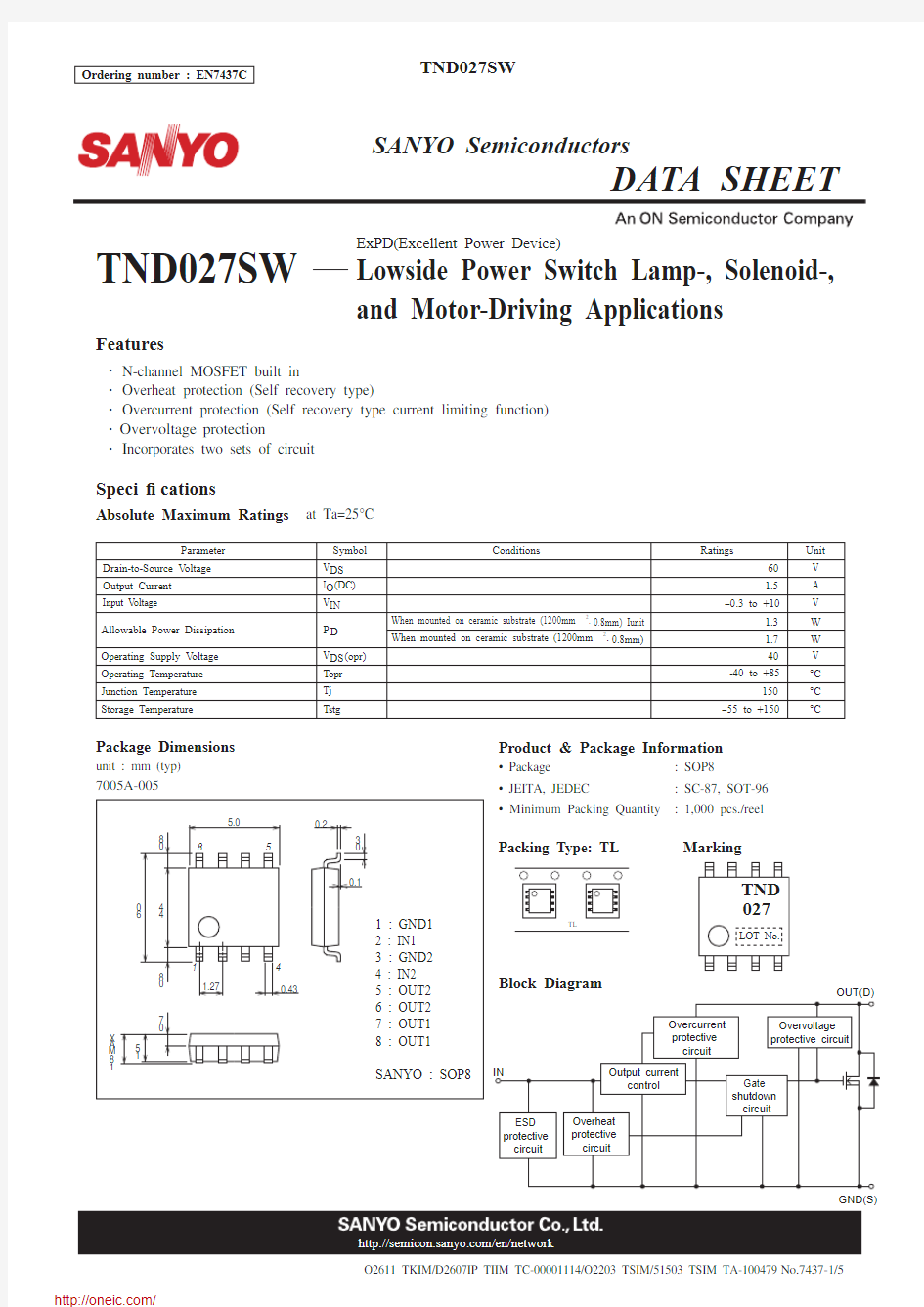
Package Dimensions
unit : mm (typ)
7005A-005
GND(S)
OUT(D)
TND027SW
ExPD(Excellent Power Device)
Lowside Power Switch Lamp-, Solenoid-,and Motor-Driving Applications
Product & Package Information
? Package : SOP8? JEITA, JEDEC : SC-87, SOT-96? Minimum Packing Quantity : 1,000 pcs./reel
Packing Type: TL Marking
Block Diagram
TND LOT No.
027
Electrical Characteristics at Ta=25°C
Parameter
Symbol Conditions
Ratings
Unit min
typ
max
Drain-to-Source Clamp Voltage V DS, clamp V IN =0V , I O =1mA 60
V Output-OFF Current I DSS 1V IN =0V , V DS =50V 10μA I DSS 2
V IN =0V , V DS =12V 5
μA Input Threshold Voltage
V IN (th)
V DS =5V , I O =1mA
1.0 1.5
2.0V Protection Circuit Operating Input Voltage V IN (opr) 410V Drain-to-Source ON Resistance R DS (on)V IN =5V , I O =1A 0.3
0.4ΩInput Current (Output On)I IN V IN =5V 0.6mA Over-Heat Detecting Temperature Tj(sd)V IN =5V , I O =1A 120150190°C Over-Current Detecting Current Is
V IN =5V 3.0 6.09.0A Over-Current Limit (Peak) I LMT
V IN =5V 3.0 6.0
9.0
A Input Clamp Voltage
V IN, clamp
I IN =1mA
10
V
Notes : 1. Overcurrent protection circuit limits the output current to the range of overcurrent limit value. 2. During overheat protecting operation, output current is turned off.
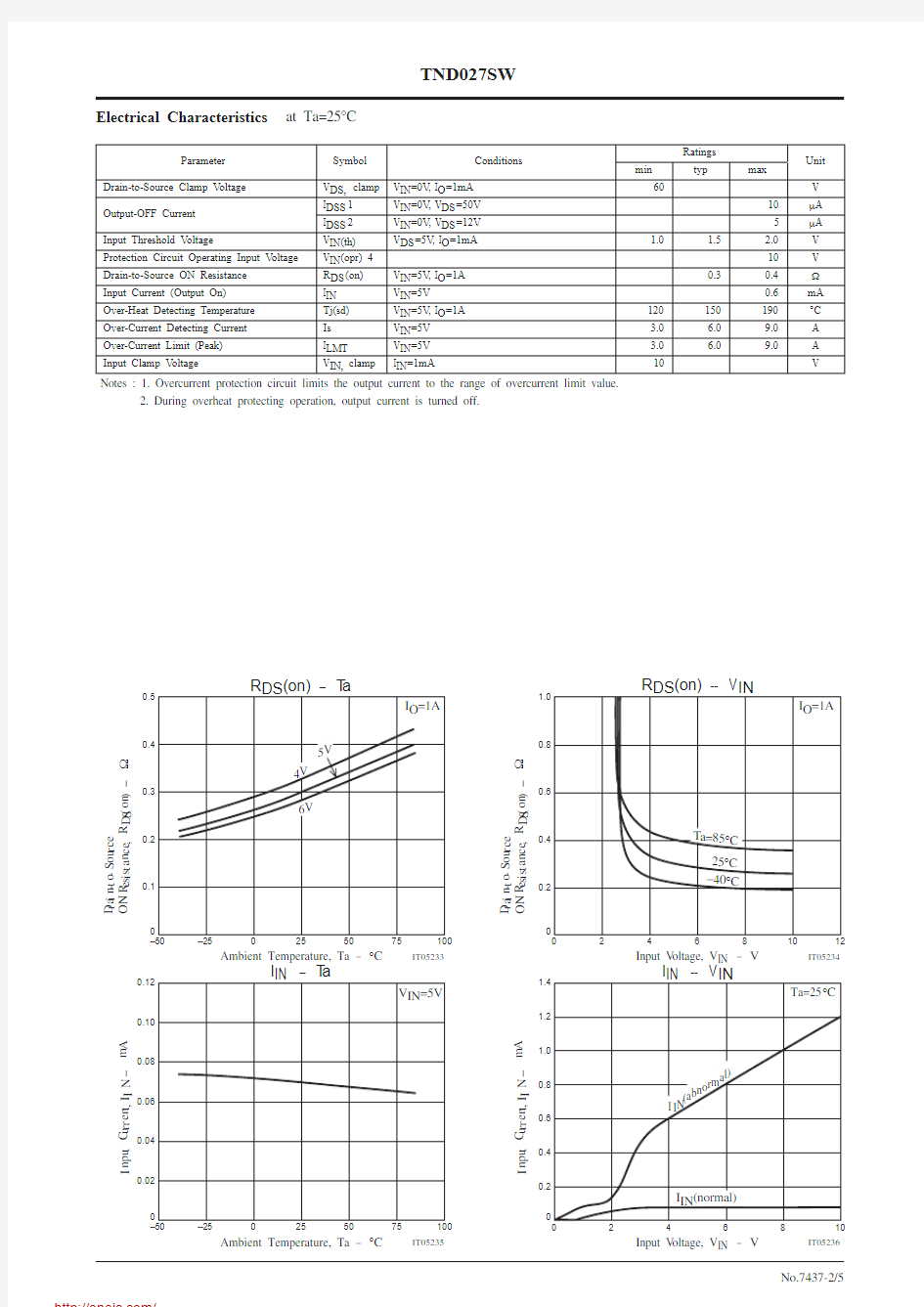
I IN -- Ta
0--50
--250255010075IT05233
IT05234
0.02
0.12
0.10
0.08
0.06
0.04
V IN =5V
D r a i n -t o -S o u r c e O N R e s i s t a n c e , R D S (o n ) -- Ω
D r a i n -t o -S o u r c e O N R e s i s t a n c e , R D S (o n ) -- Ω
Ambient Temperature, Ta -- °C
Input V oltage, V IN -- V
I n p u t C u r r e n t , I I N -- m A
I n p u t C u r r e n t , I I N -- m A
IT05241
IT05242
Ambient Temperature, Ta -- °C
Ambient Temperature, Ta
-- °C
D r a i n -t o -S o u r c e
C l a m p
V o l t a g e , V D S , C l a m p -- V
T h r e s h o l d V o l t a g e , V I N (t h ) -- V
I n p u t C l a m p V o l t a g e , V I N , C l a m p -- V
O u t p u t C u r r e n t , I O -- A
I -- Ta
IT05237
I -- V IT05238
IT05240
IT05239
Ambient Temperature, Ta -- °C
Ambient Temperature, Ta -- °C
Input V oltage, V IN -- V
Input V oltage, V IN -- V
O v e r c u r r e n t D e t e c t i n g C u r r e n t , I S -- A
O v e r c u r r e n t L i m i t , I L M T -- A
O v e r c u r r e n t L i m i t , I L M T -- A
O v e r c u r r e n t D e t e c t i n g C u r r e n t , I S -- A
4.0
4.5
142144152150148146154160158156140 5.0
5.5
6.0Tj(sd) -- V IN
IT05245
IT05247
IT05248
Ambient Temperature, Ta -- °C
O v e r h e a t D e t e c t i n g T e m p e r a t u r e , T j (s d ) -- °C
Input V oltage, V IN -- V
A l l o w a b l e P o w e r
D i s s i p a t i o n , P D -- W
A l l o w a b l e P o w e r D i s s i p a t i o n , P D (C i r c u i t 2) -- W
Allowable Power Dissipation, P D (Circuit1) -- W
Sample Application Circuit
Another Sample Application Circuit (Solenoid drive)
AC100V
AC100V
Operation Description
? The output power MOSFET will be turned on when the input voltage exceeds the input threshold voltage (4 to 6V is recommended), and then the lamp will be turned on by the current ? owing to the lamp. Conversely, the output power MOSFET will be turned off when the input voltage goes below the input threshold voltage, and the lamp will be turned off.
? The inrush current that occurs during normal lamp operation is limited to a preset value by the built-in overcurrent protecting circuit, which makes the lamp life longer.
? The internal overcurrent protection function limits the current of output power MOSFET when output current of at least the overcurrent detecting current value ? ows at load short. Besides, if the device temperature exceeds the allowable power dissipation, overheat protection function protects the power switch from being broken down by turning off the current of output power MOSFET when Tj comes to 150°C (typical).
? As an example of application circuit, DC voltage can also be controlled as a solenoid drive.
Addition
? The diode between OUT and GND in the block diagram is parasitic diode of the MOSFET.
? Not apply a voltage on IN terminal during the period when OUT voltage is lower then GND voltage when driving
a solenoid or a motor.
? Be sure connect a diode between OUT terminal and GND terminal when you want to apply a voltage on IN terminal under the above-stated state (that is, OUT V oltage < GND V oltage).
This catalog provides information as of October, 2011. Speci? cations and information herein are subject
分销商库存信息: ONSEMI
TND027SW-TL-E