MAX4927ETN+T中文资料


General Description
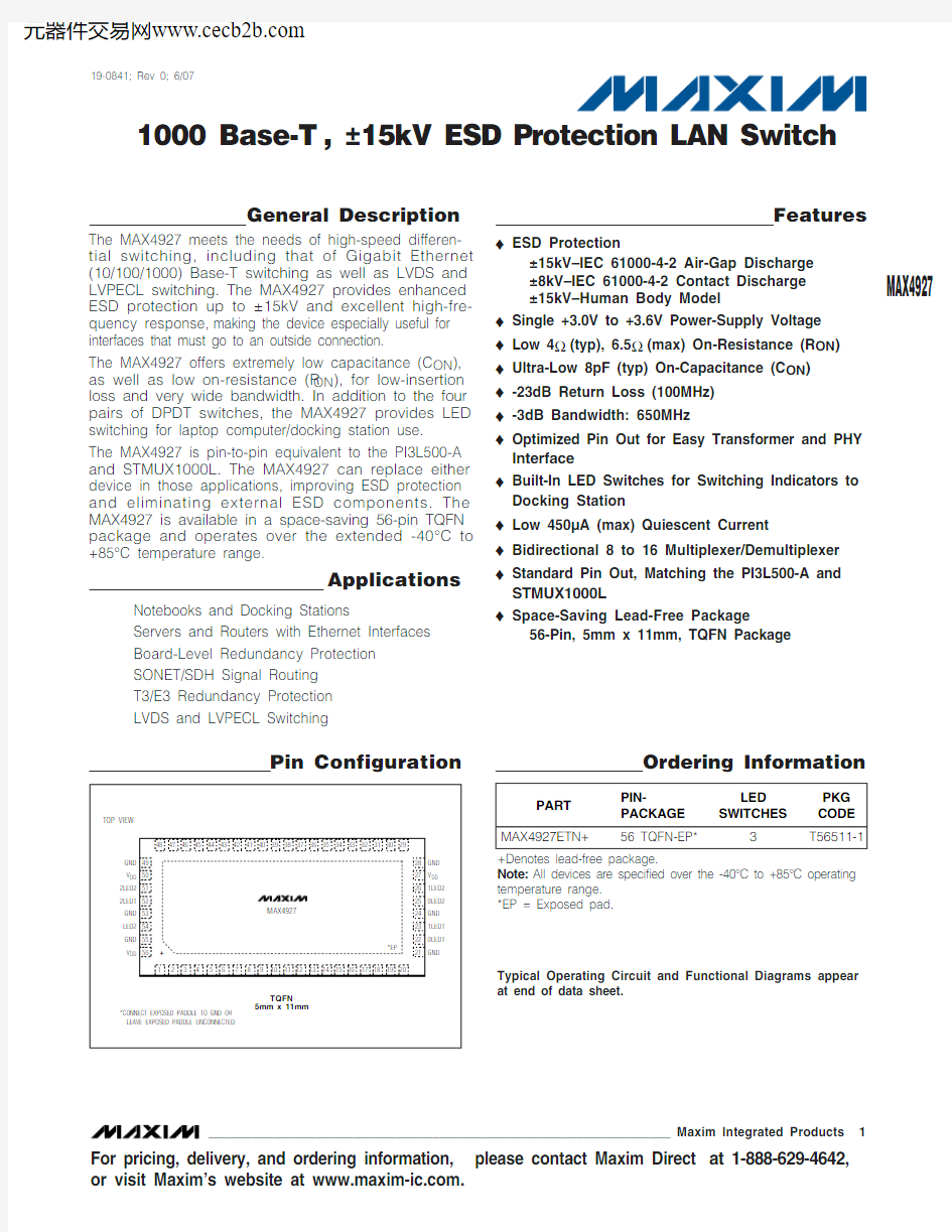
The MAX4927 meets the needs of high-speed differen-tial switching, including that of Gigabit Ethernet (10/100/1000) Base-T switching as well as LVDS and LVPECL switching. The MAX4927 provides enhanced ESD protection up to ±15kV and excellent high-fre-quency response,making the device especially useful for interfaces that must go to an outside connection.
The MAX4927 offers extremely low capacitance (C ON ),as well as low on-resistance (R ON ), for low-insertion loss and very wide bandwidth. In addition to the four pairs of DPDT switches, the MAX4927 provides LED switching for laptop computer/docking station use. The MAX4927 is pin-to-pin equivalent to the PI3L500-A and STMUX1000L. The MAX4927 can replace either device in those applications, improving ESD protection and eliminating external ESD components. The MAX4927 is available in a space-saving 56-pin TQFN package and operates over the extended -40°C to +85°C temperature range.
Applications
Notebooks and Docking Stations
Servers and Routers with Ethernet Interfaces Board-Level Redundancy Protection SONET/SDH Signal Routing T3/E3 Redundancy Protection LVDS and LVPECL Switching
Features
?ESD Protection
±15kV–IEC 61000-4-2 Air-Gap Discharge ±8kV–IEC 61000-4-2 Contact Discharge ±15kV–Human Body Model
?Single +3.0V to +3.6V Power-Supply Voltage ?Low 4Ω(typ), 6.5Ω(max) On-Resistance (R ON )?Ultra-Low 8pF (typ) On-Capacitance (C ON )?-23dB Return Loss (100MHz)?-3dB Bandwidth: 650MHz
?Optimized Pin Out for Easy Transformer and PHY Interface
?Built-In LED Switches for Switching Indicators to Docking Station ?Low 450μA (max) Quiescent Current
?Bidirectional 8 to 16 Multiplexer/Demultiplexer ?Standard Pin Out, Matching the PI3L500-A and STMUX1000L
?Space-Saving Lead-Free Package
56-Pin, 5mm x 11mm, TQFN Package
MAX4927
1000 Base-T , ±15kV ESD Protection LAN Switch
________________________________________________________________Maxim Integrated Products 1
Ordering Information
19-0841; Rev 0; 6/07
For pricing, delivery, and ordering information,please contact Maxim Direct at 1-888-629-4642,or visit Maxim’s website at https://www.360docs.net/doc/d22265042.html,.
+Denotes lead-free package.
Note:All devices are specified over the -40°C to +85°C operating temperature range.*EP = Exposed pad.
Typical Operating Circuit and Functional Diagrams appear at end of data sheet.
Pin Configuration
M A X 4927
1000 Base-T , ±15kV ESD Protection LAN Switch 2_______________________________________________________________________________________
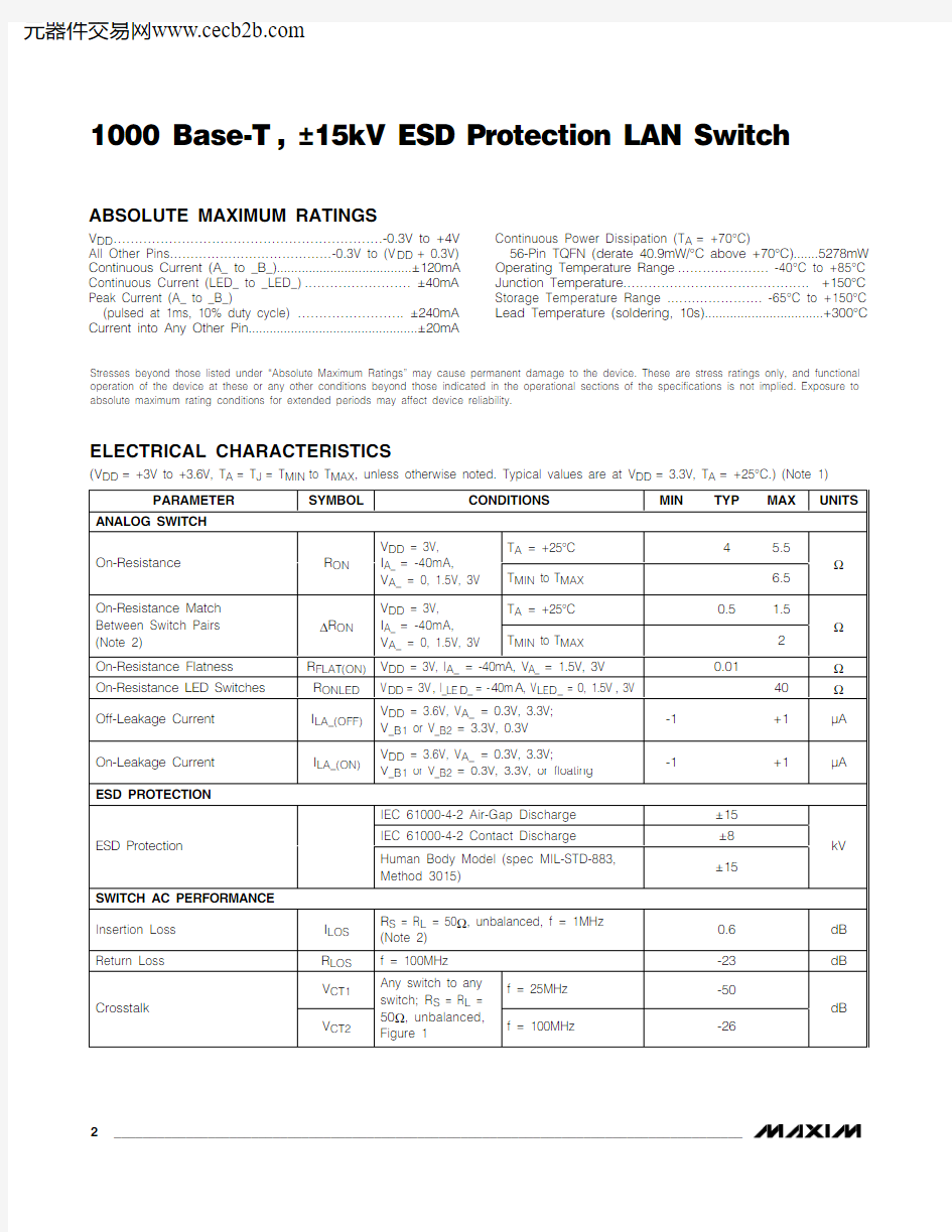
ABSOLUTE MAXIMUM RATINGS
Stresses beyond those listed under “Absolute Maximum Ratings” may cause permanent damage to the device. These are stress ratings only, and functional operation of the device at these or any other conditions beyond those indicated in the operational sections of the specifications is not implied. Exposure to absolute maximum rating conditions for extended periods may affect device reliability.
V DD ………………………………………………………-0.3V to +4V All Other Pins…………………………………-0.3V to (V DD + 0.3V)Continuous Current (A_ to _B_)......................................±120mA Continuous Current (LED_ to _LED_).…………………… ±40mA Peak Current (A_ to _B_)
(pulsed at 1ms, 10% duty cycle) ……………………. ±240mA Current into Any Other Pin................................................±20mA
Continuous Power Dissipation (T A = +70°C)
56-Pin TQFN (derate 40.9mW/°C above +70°C).......5278mW Operating Temperature Range …………………. -40°C to +85°C Junction Temperature.……………………………………. +150°C Storage Temperature Range .…………………. -65°C to +150°C Lead Temperature (soldering, 10s).................................+300°C
ELECTRICAL CHARACTERISTICS
(V DD = +3V to +3.6V, T A = T J = T MIN to T MAX , unless otherwise noted. Typical values are at V DD = 3.3V, T A = +25°C.) (Note 1)
MAX4927
1000 Base-T ±15kV ESD Protection LAN Switch
_______________________________________________________________________________________
3
ELECTRICAL CHARACTERISTICS (continued)
(V DD = +3V to +3.6V, T A = T J = T MIN to T MAX , unless otherwise noted. Typical values are at V DD = 3.3V, T A = +25°C.) (Note 1)
Figure 1. Single-Ended Bandwidth, Crosstalk, and Off-Isolation
M A X 4927
1000 Base-T , ±15kV ESD Protection LAN Switch 4_______________________________________________________________________________________
Figure 2. Turn-On and Turn-Off Times
Figure 3. Propagation Delay Times
Figure 4. Output Skew
MAX4927
1000 Base-T , ±15kV ESD Protection LAN Switch
_______________________________________________________________________________________5
0214
3560
1.0
2.0
3.0ON-RESISTANCE vs. V A_
V A_ (V)
R O N (Ω)
810121462416182220240 1.00.5 1.5 2.0 2.5 3.0
LED_ ON-RESISTANCE vs. V LED_
V LED_ (V)
R O N L E D (Ω)
0300
600
900
12001500
-40
10
-15
35
60
85
LEAKAGE CURRENT vs. TEMPERATURE
TEMPERATURE (°C)
L E A K A G E C U R R E N T (p A )
200
220240260280300320340
-40
-15
10
35
60
85
QUIESCENT SUPPLY CURRENT
vs. TEMPERATURE
TEMPERATURE (°C)
Q U I E S C E N T S U P P L Y C U R R E N T (μA )
SINGLE-ENDED INSERTION LOSS
vs. FREQUENCY
M A X 4927 t o c 05
FREQUENCY (MHz)
I N S E R T I O N L O S S (d B )
100
10
-7-8-9
-6-5-4-3-2-10
-10
1
1000
Typical Operating Characteristics
(V DD = 3.3V, T A = +25°C, unless otherwise noted.)
M A X 4927
1000 Base-T , ±15kV ESD Protection LAN Switch 6_______________________________________________________________________________________
MAX4927
1000 Base-T , ±15kV ESD Protection LAN Switch
_______________________________________________________________________________________7
Detailed Description
The MAX4927 is a high-speed analog switch targeted for 1000 Base-T applications. In a typical application,the MAX4927 switches the signals from two separate interface transformers and connects the signals to a single 1000 Base-T Ethernet PH Y (see the Typical Operating Circuit ). This configuration simplifies docking-station design by avoiding signal reflections associated with unterminated transmission lines in a T configura-tion. The MAX4927 is protected against ±15kV electro-static discharge (ESD) events. The MAX4927 also includes LED switches that allow the LED output sig-nals to be routed to a docking station along with the Ethernet signals. See the Functional Diagrams.
With its low resistance and capacitance, as well as high ESD protection, the MAX4927 can be used to switch most low-voltage differential signals, such as LVDS,SERDES, and LVPECL, as long as the signals do not exceed maximum ratings of the device.
The MAX4927switch provides an extremely low capac-itance and on-resistance to meet Ethernet insertion and return-loss specifications. The MAX4927 features three built-in LED switches.
The MAX4927incorporates a unique architecture design utilizing only n-channel switches within the main Ethernet switch, reducing I/O capacitance and channel resis-tance. An internal two-stage charge pump with a nomi-nal 7.5V output provides the high voltage needed to drive the gates of the n-channel switches while maintain-ing a consistently low R ON throughout the input signal range. An internal bandgap reference set to 1.23V and an internal oscillator running at 2.5MH z provide proper charge-pump operation. Unlike other charge-pump cir-cuits, the MAX4927 includes internal flyback capacitors,reducing design time, board space, and cost.
Digital Control Inputs
The MAX4927 provides a single digital control input,SEL. SEL controls the high-frequency switches as well as the LED switches as shown in Table 1.
Analog Signal Levels
The on-resistance of the MAX4927 is very low and sta-ble as the analog input signals are swept from ground to V DD (see the Typical Operating Characteristics ). The switches are bidirectional, allowing A_ and _B_ to be configured as either inputs or outputs.
±15kV ESD Protection
As with all Maxim devices, ESD-protection structures are incorporated on all pins to protect against electro-static discharges encountered during handling and assembly. All the high-frequency switch inputs (A_,_B_), LED switch inputs (LED_, _LED_), and SEL have high ESD protection against static electricity. Maxim’s engineers have developed state-of-the-art structures to protect these pins against ESD of ±15kV without dam-age. After an ESD event, the MAX4927 keeps working without latchup or damage.
ESD protection can be tested in various ways. All signal and control inputs of the MAX4927 are characterized for protection to the following limits:
?±15kV using the Human Body Model
?±8kV using the Contact Discharge Method specified
in IEC 61000-4-2
?±15kV using the Air-Gap Discharge Method specified
in IEC 61000-4-2ESD Test Conditions
ESD performance depends on a variety of conditions.Contact Maxim for a reliability report that documents test setup, test methodology, and test results.
M A X 4927
1000 Base-T , ±15kV ESD Protection LAN Switch 8_______________________________________________________________________________________
Human Body Model
Figure 5a shows the H uman Body Model. Figure 5b shows the current waveform it generates when dis-charged into a low impedance. This model consists of a 100pF capacitor charged to the ESD voltage of interest,which is then discharged into the test device through 1.5k Ωresistor.
IEC 61000-4-2
The IEC 61000-4-2 standard covers ESD testing and performance of finished equipment. H owever, it does not specifically refer to integrated circuits. The MAX4927helps equipment design to meet IEC 61000-4-2 without the need for additional ESD-protected components.
The major difference between tests done using the Human Body Model and IEC 61000-4-2 is higher peak current in IEC 61000-4-2 because series resistance is lower in the IEC 61000-4-2 model. Hence, the ESD with-stand voltage measured to IEC 61000-4-2 is generally lower than that measured using the H uman Body Model. Figure 5c shows the IEC 61000-4-2 model, and Figure 5d shows the current waveform for IEC 61000-4-2 ESD Contact Discharge test.
Machine Model
The machine model for ESD tests all pins using a 200pF storage capacitor and zero discharge resistance.
The objective is to emulate the stress caused when I/O pins are contacted by handling equipment during test and assembly.
The Air-Gap Discharge Method involves approaching the device with a charged probe. The Contact Discharge Method connects the probe to the device before the probe is energized.
Applications Information
Typical Operating Circuit
The Typical Operating Circuit shows the MAX4927 in a 1000 Base-T docking station application.
Power-Supply Sequencing and
Overvoltage Protection
Caution:Do not exceed the absolute maximum ratings.Stresses beyond the listed ratings may cause perma-nent damage to the device.
Proper power-supply sequencing is recommended for all CMOS devices. Always apply V DD before applying analog signals, especially if the analog signal is not current limited.
Power-Supply Bypassing
Bypass at least one V DD input to ground with a 0.1μF or larger ceramic capacitor as close to the device as pos-sible. Use the smallest physical size possible for optimal performance (0603 body size is recommended).It is also recommended to bypass more than one V DD input. A good strategy is to bypass one V DD input with a 0.1μF capacitor, and at least a second V DD input with a 10nF capacitor (use 0603 or smaller physical size ceramic capacitor).
Layout
H igh-speed switches require proper layout and design procedures for optimum performance. Keep design-con-trolled-impedance PCB traces as short as possible.Ensure that bypass capacitors are as close as possible to the device. Use large ground planes where possible.
Chip Information
PROCESS:BiCMOS
MAX4927
1000 Base-T , ±15kV ESD Protection LAN Switch
_______________________________________________________________________________________9
Figure 5a. Human Body ESD Test Model
Figure 5b. Human Body Current Waveform
Figure 5c. IEC 61000-4-2 ESD Test Model
Figure 5d. IEC 61000-4-2 ESD Generator Current Waveform
M A X 4927
1000 Base-T , ±15kV ESD Protection LAN Switch 10______________________________________________________________________________________
Typical Operating Circuit
MAX4927
1000 Base-T , ±15kV ESD Protection LAN Switch
______________________________________________________________________________________11
Functional Diagram
M A X 4927
1000 Base-T , ±15kV ESD Protection LAN Switch 12______________________________________________________________________________________
Package Information
(The package drawing(s) in this data sheet may not reflect the most current specifications. For the latest package outline information,go to https://www.360docs.net/doc/d22265042.html,/packages .)
MAX4927 1000 Base-T, ±15kV ESD Protection LAN Switch
Maxim cannot assume responsibility for use of any circuitry other than circuitry entirely embodied in a Maxim product. No circuit patent licenses are implied. Maxim reserves the right to change the circuitry and specifications without notice at any time.
Maxim Integrated Products, 120 San Gabriel Drive, Sunnyvale, CA 94086 408-737-7600 ____________________13
?2007 Maxim Integrated Products
is a registered trademark of Maxim Integrated Products, Inc. Package Information (continued)
(The package drawing(s) in this data sheet may not reflect the most current specifications. For the latest package outline information, go to https://www.360docs.net/doc/d22265042.html,/packages
.)
