1N5615GP-E354;1N5619GP-E354;1N5617GP-E354;1N5621GP-E354;1N5623GP-E354;中文规格书,Datasheet资料
Document Number: 88522For technical questions within your region, please contact one of the following:https://www.360docs.net/doc/de14240387.html, Glass Passivated Junction Fast Switching Rectifier
1N5615GP thru 1N5623GP
Vishay General Semiconductor
FEATURES
?Superectifier structure for high reliability condition
?Cavity-free glass-passivated junction ?Fast switching for high efficiency ?Low leakage current
?High forward surge capability
?Meets environmental standard MIL-S-19500?Solder dip 275 °C max. 10 s, per JESD 22-B106
?AEC-Q101 qualified
?Compliant to RoH S Directive 2002/95/EC and in accordance to WEEE 2002/96/EC
TYPICAL APPLICATIONS
For use in fast switching rectification of power supply,inverters, converters and freewheeling diodes for consumer,automotive and telecommunication.
MECHANICAL DATA
Case: DO-204AC, molded epoxy over glass body
Molding compound meets UL 94 V-0 flammability rating Base P/N-E3 - RoHS compliant, commercial grade Base P/NHE3 - RoHS compliant, AEC-Q101 qualified Terminals: Matte tin plated leads, solderable per J-STD-002 and JESD 22-B102
E3 suffix meets JESD 201 class 1A whisker test, HE3 suffix meets JESD 201 class 2 whisker test Polarity: Color band denotes cathode end
PRIMARY CHARACTERISTICS
I F(AV) 1.0 A V RRM 200 V to 1000 V
I FSM 50 A
t rr 150 ns, 250 ns, 300 ns, 500 ns
I R 0.5 μA V F 1.2 V T J max.
175 °C
DO-204AC (DO-15)
SUPERECTIFIER ?
MAXIMUM RATINGS (T A = 25°C unless otherwise noted)
PARAMETER
SYMBOL 1N5615GP
1N5617GP
1N5619GP
1N5621GP
1N5623GP UNIT Maximum repetitive peak reverse voltage V RRM 2004006008001000V Maximum RMS voltage V RMS 140280420560700V Maximum DC blocking voltage
V DC 200
400
600800
1000
A Maximum average forward rectified current 0.375" (9.5 mm) lead length at T A = 55 °C I F(AV) 1.0A Peak forward surge current 8.3 ms single half sine-wave superimposed on rated load I FSM 50A Operating junction and storage temperature range
T J , T STG
- 65 to + 175
°C
https://www.360docs.net/doc/de14240387.html, For technical questions within your region, please contact one of the following:Document Number: 885221N5615GP thru 1N5623GP
Vishay General Semiconductor
Note
(1)Thermal resistance from junction to ambient at 0.375" (9.5 mm) lead length, P.C.B. mounted
Note
(1)AEC-Q101 qualified
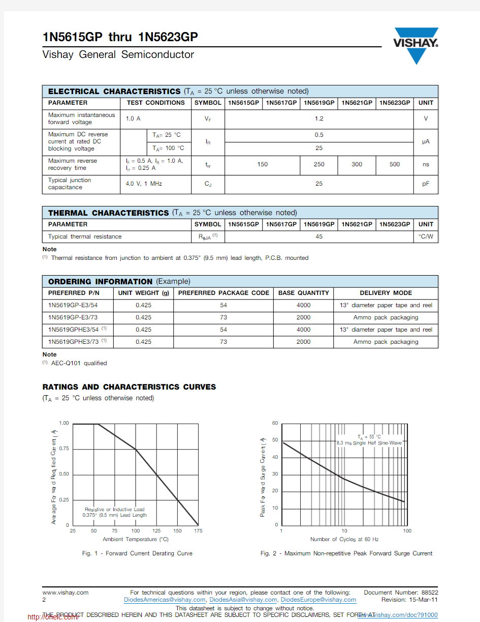
RATINGS AND CHARACTERISTICS CURVES
(T A = 25 °C unless otherwise noted)
Fig. 1 - Forward Current Derating Curve Fig. 2 - Maximum Non-repetitive Peak Forward Surge Current
ELECTRICAL CHARACTERISTICS (T A = 25°C unless otherwise noted)
PARAMETER
TEST CONDITIONS SYMBOL
1N5615GP
1N5617GP
1N5619GP
1N5621GP
1N5623GP
UNIT Maximum instantaneous forward voltage 1.0 A
V F 1.2V
Maximum DC reverse current at rated DC blocking voltage T A = 25 °C I R 0.5μA
T A = 100 °C
25Maximum reverse recovery time I F = 0.5 A, I R = 1.0 A,I rr = 0.25 A t rr 150
250300
500
ns Typical junction capacitance
4.0 V, 1 MHz
C J
25
pF
THERMAL CHARACTERISTICS (T A = 25°C unless otherwise noted)
PARAMETER
SYMBOL 1N5615GP
1N5617GP
1N5619GP
1N5621GP
1N5623GP
UNIT Typical thermal resistance
R JA (1)
45
°C/W
ORDERING INFORMATION (Example)
PREFERRED P/N UNIT WEIGHT (g)
PREFERRED PACKAGE CODE
BASE QUANTITY
DELIVERY MODE
1N5619GP-E3/540.42554400013" diameter paper tape and reel
1N5619GP-E3/730.425732000Ammo pack packaging 1N5619GPHE3/54 (1)0.42554400013" diameter paper tape and reel
1N5619GPHE3/73 (1)0.425
73
2000
Ammo pack packaging
Document Number: 88522For technical questions within your region, please contact one of the following:https://www.360docs.net/doc/de14240387.html, 1N5615GP thru 1N5623GP
Vishay General Semiconductor
Fig. 3 - Typical Instantaneous Forward Characteristics Fig. 4 - Typical Reverse Characteristics Fig. 5 - Typical Junction Capacitance
Fig. 6 - Typical Transient Thermal Impedance
PACKAGE OUTLINE DIMENSIONS
Legal Disclaimer Notice https://www.360docs.net/doc/de14240387.html, Vishay
Disclaimer
ALL PRODU CT, PRODU CT SPECIFICATIONS AND DATA ARE SU BJECT TO CHANGE WITHOU T NOTICE TO IMPROVE RELIABILITY, FUNCTION OR DESIGN OR OTHERWISE.
Vishay Intertechnology, Inc., its affiliates, agents, and employees, and all persons acting on its or their behalf (collectively,“Vishay”), disclaim any and all liability for any errors, inaccuracies or incompleteness contained in any datasheet or in any other disclosure relating to any product.
Vishay makes no warranty, representation or guarantee regarding the suitability of the products for any particular purpose or the continuing production of any product. To the maximum extent permitted by applicable law, Vishay disclaims (i) any and all liability arising out of the application or use of any product, (ii) any and all liability, including without limitation special, consequential or incidental damages, and (iii) any and all implied warranties, including warranties of fitness for particular purpose, non-infringement and merchantability.
Statements regarding the suitability of products for certain types of applications are based on Vishay’s knowledge of typical requirements that are often placed on Vishay products in generic applications. Such statements are not binding statements about the suitability of products for a particular application. It is the customer’s responsibility to validate that a particular product with the properties described in the product specification is suitable for use in a particular application. Parameters provided in datasheets and/or specifications may vary in different applications and performance may vary over time. All operating parameters, including typical parameters, must be validated for each customer application by the customer’s technical experts. Product specifications do not expand or otherwise modify Vishay’s terms and conditions of purchase, including but not limited to the warranty expressed therein.
Except as expressly indicated in writing, Vishay products are not designed for use in medical, life-saving, or life-sustaining applications or for any other application in which the failure of the Vishay product could result in personal injury or death. Customers using or selling Vishay products not expressly indicated for use in such applications do so at their own risk and agree to fully indemnify and hold Vishay and its distributors harmless from and against any and all claims, liabilities, expenses and damages arising or resulting in connection with such use or sale, including attorneys fees, even if such claim alleges that Vishay or its distributor was negligent regarding the design or manufacture of the part. Please contact authorized Vishay personnel to obtain written terms and conditions regarding products designed for such applications.
No license, express or implied, by estoppel or otherwise, to any intellectual property rights is granted by this document or by any conduct of Vishay. Product names and markings noted herein may be trademarks of their respective owners.
Material Category Policy
Vishay Intertechnology, Inc. hereb y certifies that all its products that are identified as RoHS-Compliant fulfill the definitions and restrictions defined under Directive 2011/65/EU of The European Parliament and of the Council of June 8, 2011 on the restriction of the use of certain hazardous substances in electrical and electronic equipment (EEE) - recast, unless otherwise specified as non-compliant.
Please note that some Vishay documentation may still make reference to RoHS Directive 2002/95/EC. We confirm that all the products identified as being compliant to Directive 2002/95/EC conform to Directive 2011/65/EU.
Revision: 12-Mar-121Document Number: 91000
分销商库存信息:
VISHAY-GENERAL-SEMICONDUCTOR
1N5615GP-E3/541N5619GP-E3/541N5617GP-E3/54 1N5621GP-E3/541N5623GP-E3/541N5617GP-E3/73 1N5621GP-E3/731N5615GPHE3/541N5617GPHE3/54 1N5619GPHE3/541N5621GPHE3/541N5623GPHE3/54