MAX3468ESA中文资料
General Description
The MAX3465–MAX3469 are high-speed differential bus transceivers for RS-485 and RS-422 communica-tions. They are designed to meet TIA/EIA-422-B,TIA/EIA-485-A, V.11, and X.27 standards. The trans-ceiver complies with the Profibus specification provid-ing +2.1V minimum output level with a 54?load,40Mbps data rate, and output skew less than 2ns. Each part contains one three-state differential line driver and one differential input line receiver. The devices operate from a +5V supply and feature true fail-safe circuitry,which guarantees a logic-high receiver output when the receiver inputs are open or shorted. This enables all receiver outputs on a terminated bus to output logic highs when all transmitters are disabled.
All devices feature a 1/4-standard-unit load receiver input impedance that allows 128 transceivers on the bus. Driver and receiver propagation delays are guar-anteed under 20ns for multidrop, clock distribution applications. Drivers are short-circuit current limited and are protected against excessive power dissipation by thermal-shutdown circuitry. The driver and receiver feature active-high and active-low enables, respective-ly, that can be connected together externally to serve as a direction control.
Applications
High-Speed RS-485 Communications High-Speed RS-422 Communications Level Translators
Industrial-Control Local Area Networks Profibus Applications
Features
?Recommended for Profibus Applications
?Up to 40Mbps Data Rate
?15ns Transmitter Propagation Delay ?20ns Receiver Propagation Delay ?2ns Transmitter and Receiver Skew
?High Differential Driver Output Level (2.1V on 54?)?Hot-Swap Versions
?1μA Shutdown Supply Current
?Low Supply Current Requirements (2.5mA, typ)?Allow Up to 128 Transceivers on the Bus
?True Fail-Safe Receiver while Maintaining EIA/TIA-485 Compatibility ?Designed for Multipoint Transmissions on Long or Noisy Bus Lines ?Full-Duplex and Half-Duplex Versions Available ?Phase Controls to Correct for Twisted-Pair Reversal for 14-Pin Versions ?Current-Limiting and Thermal Shutdown for Driver Overload Protection
MAX3465–MAX3469
+5V , Fail-Safe, 40Mbps, Profibus RS-485/
RS-422 Transceivers
Ordering Information
19-3038; Rev 1; 1/04
For pricing, delivery, and ordering information,please contact Maxim/Dallas Direct!at 1-888-629-4642, or visit Maxim’s website at https://www.360docs.net/doc/e3855955.html,.
Ordering Information continued at end of data sheet.Pin Configurations appear at end of data sheet.
M A X 3465–M A X 3469
+5V , Fail-Safe, 40Mbps, Profibus RS-485/RS-422 Transceivers 2_______________________________________________________________________________________
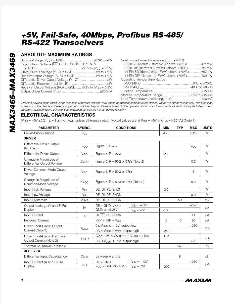
ABSOLUTE MAXIMUM RATINGS
ELECTRICAL CHARACTERISTICS
Stresses beyond those listed under “Absolute Maximum Ratings” may cause permanent damage to the device. These are stress ratings only, and functional operation of the device at these or any other conditions beyond those indicated in the operational sections of the specifications is not implied. Exposure to absolute maximum rating conditions for extended periods may affect device reliability.
Supply Voltage (V CC ) to GND..................................-0.3V to +6V Control Input Voltage (RE , DE, DI, SHDN, TXP, RXP)
to GND....................................................-0.3V to (V CC + 0.3V)Driver Output Voltage (Y, Z) to GND.........................-8V to +13V Receiver Input Voltage (A, B) to GND.......................-8V to +13V Differential Driver Output Voltage (Y - Z)...............................±8V Differential Receiver Input (A - B)..........................................±8V Receiver Output Voltage (RO) to GND.......-0.3V to (V CC + 0.3V)Output Driver Current (Y, Z)...........................................±250mA
Continuous Power Dissipation (T A = +70°C)
8-Pin SO (derate 5.88mW/°C above +70°C)................471mW 8-Pin DIP (derate 9.09mW/°C above +70°C)...............727mW 14-Pin SO (derate 8.33mW/°C above +70°C)..............667mW 14-Pin DIP (derate 10mW/°C above +70°C)................800mW Operating Temperature Range
MAX346_C__......................................................0°C to +70°C MAX346_E__....................................................-40°C to +85°C Junction Temperature......................................................+150°C Storage Temperature Range.............................-65°C to +150°C Lead Temperature (soldering, 10s).................................+300°C
MAX3465–MAX3469
+5V , Fail-Safe, 40Mbps, Profibus RS-485/
RS-422 Transceivers
_______________________________________________________________________________________3
ELECTRICAL CHARACTERISTICS (continued)
Note 2:?V OD and ?V OC are the changes in V OD and V OC , respectively, when the DI input changes state.
Note 3:The short-circuit output current applies to peak current just prior to foldback-current limiting; the short-circuit foldback output
current applies during current limiting to allow a recovery from bus contention.
Note 4:Capacitive load includes test probe and fixture capacitance.
Note 5:Shutdown is enabled by bringing RE high and DE low or by bringing SHDN high. If the enable inputs are in this state for less
than 50ns, the device is guaranteed not to enter shutdown. If the enable inputs are in this state for at least 800ns, the device is guaranteed to have entered shutdown.
M A X 3465–M A X 3469
+5V , Fail-Safe, 40Mbps, Profibus RS-485/RS-422 Transceivers 4_______________________________________________________________________________________
ELECTRICAL CHARACTERISTICS (continued)
(V CC = +5V ±5%, T A = T MIN to T MAX , unless otherwise noted. Typical values are at V CC = +5V and T A = +25°C.) (Note 1)
NO-LOAD SUPPLY CURRENT
vs. TEMPERATURE
TEMPERATURE (°C)
N O -L O A D S U P P L Y C U R R E N T (m A )
60
40
-20
20
2.152.202.252.302.352.402.452.502.10
-40
80
OUTPUT CURRENT
vs. RECEIVER OUTPUT LOW VOLTAGE
M A X 3465 t o c 02
OUTPUT LOW VOLTAGE (V)
O U T P U T C U R R E N T (m A )
4.54.03.53.02.52.01.51.00.510203*********
5.0
OUTPUT CURRENT
vs. RECEIVER OUTPUT HIGH VOLTAGE
M A X 3465 t o c 03
OUTPUT HIGH VOLTAGE (V)
O U T P U T C U R R E N T (m A )
43215101520253035
05
Typical Operating Characteristics
(V CC = +5V, T A = +25°C, unless otherwise noted.)
MAX3465–MAX3469
+5V , Fail-Safe, 40Mbps, Profibus RS-485/
RS-422 Transceivers
_______________________________________________________________________________________5
RECEIVER PROPAGATION DELAY
vs. TEMPERATURE
M A X 3465 t o c 07
TEMPERATURE (°C)
P R O P A G A T I O N D E L A Y (n s )
60
35
10
-15
12
14
16
18
2010-40
85
DRIVER PROPAGATION DELAY
vs. TEMPERATURE
TEMPERATURE (°C)
P R O P A G A T I O N D E L A Y (n s )
60
35
10
-15
6
8
10
12
4
-40
85
DRIVER DIFFERENTIAL OUTPUT VOLTAGE
vs. TEMPERATURE
TEMPERATURE (°C)
O U T P U T V O L T A G E (V )
60
35
10
-15
2.5
3.0
3.5
2.0-40
85
DRIVER OUTPUT CURRENT
vs. DIFFERENTIAL OUTPUT VOLTAGE
M A X 3465 t o c 10
DIFFERENTIAL OUTPUT VOLTAGE (V)
O U T P U T C U R R E N T (m A )
4
3
2
1
1
10
1000.1
5
OUTPUT CURRENT
vs. DRIVER OUTPUT LOW VOLTAGE
M A X 3465 t o c 11
OUTPUT LOW VOLTAGE (V)
O U T P U T C U R R E N T (m A )
9
6
3
40
80
120
16020000
12
-160
-120
-80
-40
0-7
-1
-5
-3
1
3
5
OUTPUT CURRENT
vs. DRIVER OUTPUT HIGH VOLTAGE
OUTPUT HIGH VOLTAGE (V)
O U T P U T C U R R E N T (m A )
Typical Operating Characteristics (continued)
(V CC = +5V, T A = +25°C, unless otherwise noted.)
SHUTDOWN SUPPLY CURRENT
vs. TEMPERATURE
M A X 3465 t o c 04
TEMPERATURE (°C)S H U T D O W N S U P P L Y C U R R E N T (n A )
60
35
10
-15
501001502002503000-40
85RECEIVER OUTPUT LOW VOLTAGE
vs. TEMPERATURE
TEMPERATURE (°C)R E C E I V E R O U T P U T L O W V O L T A G E (m V )
603510-157510012515017520050
-4085RECEIVER OUTPUT HIGH VOLTAGE
vs. TEMPERATURE
TEMPERATURE (°C)
R E C E I V E R O U T P U T H I G H V O L T A G E (m V )
603510-154.654.704.754.804.854.904.60
-4085
M A X 3465–M A X 3469
+5V , Fail-Safe, 40Mbps, Profibus RS-485/RS-422 Transceivers
Typical Operating Characteristics (continued)
(V CC = +5V, T A = +25°C, unless otherwise noted.)
DRIVER AND RECEIVER PROPAGATION DELAYS
MAX3465 toc13
10ns/div
5V/div 5V/div
2V/div
Y, Z DI RO R DIFF = 54?
DATA RATE = 20Mbps ENABLE RESPONSE TIME
MAX3465 toc14
20ns/div
5V/div 1V/div
Y, Z DE
R DIFF = 54?
EYE DIAGRAM
MAX3465 toc15
10ns/div
1V/div
Y, Z R DIFF = 54?
DATA RATE = 20Mbps
MAX3465–MAX3469
+5V , Fail-Safe, 40Mbps, Profibus RS-485/
RS-422 Transceivers
_______________________________________________________________________________________7
MAX3465/MAX3466
Function Tables
MAX3467
MAX3468/MAX3469
M A X 3465–M A X 3469
+5V , Fail-Safe, 40Mbps, Profibus RS-485/RS-422 Transceivers 8
_______________________________________________________________________________________
Pin Configurations and Typical Operating Circuit
Figure 1. MAX3465/MAX3466 Pin Configuration and Typical Full-Duplex Operating Circuit
Figure 2. MAX3467 Pin Configuration and Typical Full-Duplex Operating Circuit
Figure 3. MAX3468/MAX3469 Pin Configuration and Typical Full-Duplex Operating Circuit
MAX3465–MAX3469
+5V , Fail-Safe, 40Mbps, Profibus RS-485/
RS-422 Transceivers
_______________________________________________________________________________________9
Detailed Description
The MAX3465–MAX3469 high-speed transceivers for RS-485/RS-422 communication contain one driver and one receiver. These devices feature true fail-safe cir-cuitry, which guarantees a logic-high receiver output when the receiver inputs are open or shorted, or when they are connected to a terminated transmission line with all drivers disabled (see the True Fail-Safe sec-tion). The MAX3465–MAX3469’s driver slew rates allow transmit speeds up to 40Mbps.
The MAX3468 and MAX3469 are half-duplex trans-ceivers, while the MAX3465, MAX3466, and MAX3467are full-duplex transceivers. All of these parts operate from a single +5V supply. Drivers are output short-cir-cuit current limited. Thermal-shutdown circuitry protects drivers against excessive power dissipation. When acti-vated, the thermal-shutdown circuitry places the driver outputs into a high-impedance state. The MAX3465and MAX3468 devices have a hot-swap input structure that prevents disturbances on the differential signal lines when a circuit board is plugged into a hot back-plane (see the Hot-Swap Capability section). All devices have output levels that are compatible with Profibus standards.
True Fail-Safe
The MAX3465–MAX3469 guarantee a logic-high receiv-er output when the receiver inputs are shorted or open,or when they are connected to a terminated transmis-sion line with all drivers disabled. This is done by set-ting the receiver threshold between -50mV and -200mV. If the differential receiver input voltage (A - B)is greater than or equal to -50mV, RO is logic high. If A - B is less than or equal to -200mV, RO is logic low. In the case of a terminated bus with all transmitters dis-abled, the receiver’s differential input voltage is pulled to 0V by the termination. With the receiver thresholds of the MAX3465–MAX3469, this results in a logic high with a 50mV minimum noise margin. Unlike previous true fail-safe devices, the -50mV to -200mV threshold com-plies with the ±200mV EIA/TIA-485 standard.
Hot-Swap Capability
Hot-Swap Inputs
When circuit boards are inserted into a “hot” or pow-ered backplane, disturbances to the enable and differ-ential receiver inputs can lead to data errors. Upon initial circuit board insertion, the processor undergoes its power-up sequence. During this period, the proces-sor output drivers are high impedance and are unable to drive the DE input of the MAX3465/MAX3468 to a
defined logic level. Leakage currents up to 10μA from the high-impedance output could cause DE to drift to an incorrect logic state. Additionally, parasitic circuit board capacitance could cause coupling of V CC or GND to DE.These factors could improperly enable the driver.
When V CC rises, an internal pulldown circuit holds DE low for around 15μs. After the initial power-up sequence, the pulldown circuit becomes transparent,resetting the hot-swap-tolerable input.
Hot-Swap Input Circuitry
The MAX3465/MAX3468 enable inputs feature hot-swap capability. At the input there are two NMOS devices, M1and M2 (Figure 4). When V CC ramps from 0, an internal 15μs timer turns on M2 and sets the SR latch, which also turns on M1. Transistors M2, a 2mA current sink,and M1, a 100μA current sink, pull DE to GND through a 5.6k ?resistor. M2 is designed to pull DE to the disabled state against an external parasitic capacitance up to 100pF that can drive DE high. After 15μs, the timer deactivates M2 while M1 remains on, holding DE low against three-state leakages that can drive DE high. M1remains on until an external source overcomes the required input current. At this time, the SR latch resets and M1 turns off. When M1 turns off, DE reverts to a standard, high-impedance CMOS input. Whenever V CC drops below 1V, the hot-swap input is reset.
For RE there is a complementary circuit employing two PMOS devices pulling to V CC .
Figure 4. Simplified Structure of the Driver Enable Pin (DE)
M A X 3465–M A X 3469
+5V , Fail-Safe, 40Mbps, Profibus RS-485/RS-422 Transceivers 10______________________________________________________________________________________
Figure 5. Driver DC Test Load
Figure 7. Driver Propagation Delays
Figure 9. Driver Enable and Disable Times
Figure 10. Receiver Propagation Delays
Figure 11. Receiver Enable and Disable Times
Figure 8. Enable/Disable Timing Test Load
MAX3465–MAX3469
+5V , Fail-Safe, 40Mbps, Profibus RS-485/
RS-422 Transceivers
______________________________________________________________________________________11
Applications Information
128 Transceivers on the Bus
The standard RS-485 receiver input impedance is 12k ?(one unit load), and the standard driver can drive up to 32 unit loads. The MAX3465–MAX3469 family of trans-ceivers has a 1/4-unit-load receiver input impedance (48k ?), allowing up to 128 transceivers to be connect-ed in parallel on one communication line. Any combina-tion of these devices and/or other RS-485 transceivers with a total of 32 unit loads or less can be connected to the line.
Low-Power Shutdown Mode
(Except MAX3467)
Low-power shutdown mode is initiated by bringing SHDN high (MAX3465/MAX3466), or both RE high and DE low. In shutdown, the devices typically draw only 1μA of supply current. RE and DE can be driven simul-taneously; the devices are guaranteed not to enter shut-down if RE is high and DE is low for less than 50ns. If the inputs are in this state for at least 800ns, the devices are guaranteed to enter shutdown.
Driver Output Protection
Two mechanisms prevent excessive output current and power dissipation caused by faults or by bus con-tention. The first, a foldback current limit on the output stage, provides immediate protection against short cir-cuits over the whole common-mode voltage range (see the Typical Operating Characteristics ). The second, a thermal-shutdown circuit, forces the driver outputs into a high-impedance state if the die temperature exceeds +140°C.
Propagation Delay
Many digital encoding schemes depend on the difference between the driver and receiver propagation delay times.Typical propagation delays are shown in the Typical Operating Characteristics . The difference in receiver delay times, |t PLH - t PHL |, is a maximum of 2ns. The driver skew time |t PLH - t PHL | is also a maximum of 2ns.
Typical Applications
The MAX3465–MAX3469 transceivers are designed for bidirectional data communications on multipoint bus transmission lines. Figures 13 and 14 show typical net-work applications circuits. To minimize reflections, the line should be terminated at both ends in its character-istic impedance, and stub lengths off the main line should be kept as short as possible.
Profibus Termination
The MAX3465–MAX3469 are designed for driving Profibus termination networks. With a worst-case load-ing of two termination networks with 220?termination impedance and 390?pullups and pulldowns, the dri-vers can drive V A-B > 2.1V output.
Chip Information
TRANSISTOR COUNT: 610PROCESS: BiCMOS
Figure 12. Receiver Propagation Delay Test Circuit
Ordering Information (continued)
M A X 3465–M A X 3469
+5V , Fail-Safe, 40Mbps, Profibus RS-485/RS-422 Transceivers 12______________________________________________________________________________________
Figure 13. Typical Half-Duplex RS-485 Network
Figure 14. Typical Full-Duplex RS-485 Network
MAX3465–MAX3469
+5V , Fail-Safe, 40Mbps, Profibus RS-485/
RS-422 Transceivers
______________________________________________________________________________________13
Package Information
(The package drawing(s) in this data sheet may not reflect the most current specifications. For the latest package outline information,go to https://www.360docs.net/doc/e3855955.html,/packages .)
M A X 3465–M A X 3469
+5V , Fail-Safe, 40Mbps, Profibus RS-485/RS-422 Transceivers Maxim cannot assume responsibility for use of any circuitry other than circuitry entirely embodied in a Maxim product. No circuit patent licenses are implied. Maxim reserves the right to change the circuitry and specifications without notice at any time.
14____________________Maxim Integrated Products, 120 San Gabriel Drive, Sunnyvale, CA 94086 408-737-7600?2004 Maxim Integrated Products
Printed USA
is a registered trademark of Maxim Integrated Products.
P D I P N .E P
S
Package Information (continued)
(The package drawing(s) in this data sheet may not reflect the most current specifications. For the latest package outline information,go to https://www.360docs.net/doc/e3855955.html,/packages .)