5SNA 1600N170100_1700_1600-ABB
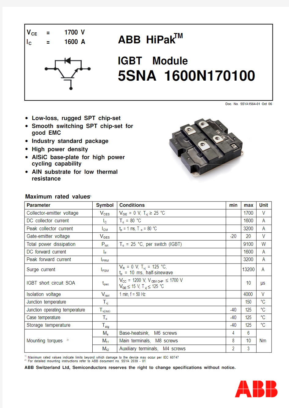
ABB Switzerland Ltd, Semiconductors reserves the right to change specifications without notice.
Doc. No. 5SYA1564-01 Oct 06
? Low-loss, rugged SPT chip-set ? Smooth switching SPT chip-set for good EMC
? Industry standard package ? High power density
? AlSiC base-plate for high power cycling capability
? AlN substrate for low thermal resistance
Maximum rated values 1)
Parameter
Symbol Conditions min max Unit Collector-emitter voltage V CES V GE = 0 V, T vj ≥ 25 °C 1700 V DC collector current I C T c = 80 °C 1600 A Peak collector current I CM t p = 1 ms, T c = 80 °C 3200 A Gate-emitter voltage V GES
-20 20 V Total power dissipation P tot T c = 25 °C, per switch (IGBT) 9100 W DC forward current I F 1600 A Peak forward current I FRM
3200
A
Surge current
I FSM V R = 0 V, T vj = 125 °C, t p = 10 ms, half-sinewave 13200 A IGBT short circuit SOA t psc V CC = 1200 V, V CEM CHIP ≤ 1700 V V GE ≤ 15 V, T vj ≤ 125 °C 10
μs
Isolation voltage V isol 1 min, f = 50 Hz 4000 V Junction temperature
T vj 150 °C Junction operating temperature T vj(op) -40 125 °C Case temperature T c -40 125 °C Storage temperature T stg
-40 125 °C
M s Base-heatsink, M6 screws 4 6 M t1 Main terminals, M8 screws 8 10 Mounting torques 2)
M t2
Auxiliary terminals, M4 screws
2
3
Nm
1)
Maximum rated values indicate limits beyond which damage to the device may occur per IEC 60747 2)
For detailed mounting instructions refer to ABB document no. 5SYA 2039 - 01
Parameter Symbol Conditions
min typ max Unit Collector (-emitter) breakdown voltage V (BR)CES V GE = 0 V, I C = 10 mA, T vj = 25 °C 1700 V T vj = 25 °C 2.0 2.3 2.6 V Collector-emitter 4) saturation voltage V CE sat I C = 1600 A, V GE = 15 V T vj = 125 °C 2.3 2.6 2.9 V T vj = 25 °C 8 mA Collector cut-off current I CES V CE = 1700 V, V GE = 0 V
T vj = 125 °C
80 mA Gate leakage current I GES V CE = 0 V, V GE = ±20 V, T vj = 125 °C -500 500 nA Gate-emitter threshold voltage V GE(TO) I C = 160 mA, V CE = V GE , T vj = 25 °C 4.5 6.5 V Gate charge Q ge I C = 1600 A, V CE = 900 V, V GE = -15 V .. 15 V
14.6 μC
Input capacitance C ies 152 Output capacitance
C oes 14.6 Reverse transfer capacitance C res V CE = 25 V, V GE = 0 V, f = 1 MHz, T vj = 25 °C
6.4 nF T vj = 25 °C 290 Turn-on delay time t d(on) T vj = 125 °C 300 ns T vj = 25 °C 175 Rise time
t r V CC = 900 V, I C = 1600 A, R G = 0.82 ?, V GE = ±15 V,
L σ = 50 nH, inductive load T vj = 125 °C 190 ns T vj = 25 °C 1050 Turn-off delay time t d(off) T vj = 125 °C 1140 ns T vj = 25 °C 150 Fall time
t f
V CC = 900 V, I C = 1600 A, R G = 0.82 ?, V GE = ±15 V,
L σ = 50 nH, inductive load T vj = 125 °C 170 ns T vj = 25 °C 380 Turn-on switching energy E on V CC = 900 V, I C = 1600 A, V GE = ±15 V, R G = 0.82 ?, L σ = 50 nH, inductive load T vj = 125 °C 530 mJ
T vj = 25 °C 460 Turn-off switching energy E off V CC = 900 V, I C = 1600 A, V GE = ±15 V, R G = 0.82 ?, L σ = 50 nH, inductive load
T vj = 125 °C
590 mJ Short circuit current I SC t psc ≤ 10 μs, V GE = 15 V, T vj = 125 °C, V CC = 1200 V, V CEM CHIP ≤ 1700 V 7200 A Module stray inductance L σ CE
15 nH T C = 25 °C 0.10 Resistance, terminal-chip
R CC’+EE’
T C = 125 °C
0.13
m ?
3) Characteristic values according to IEC 60747 – 9
4)
Collector-emitter saturation voltage is given at chip level
Parameter Symbol Conditions min
typ max Unit T vj = 25 °C 1.65 2.0 Forward voltage 6) V F I F = 1600 A
T vj = 125 °C 1.7 2.0 V T vj = 25 °C
1090 Reverse recovery current I rr T vj = 125 °C 1400 A T vj = 25 °C 390 Recovered charge Q rr T vj = 125 °C 690 μC T vj = 25 °C 620 Reverse recovery time t rr T vj = 125 °C 830 ns T vj = 25 °C 280 Reverse recovery energy
E rec
V CC = 900 V, I F = 1600 A, V GE = ±15 V, R G = 0.82 ? L σ = 50 nH inductive load
T vj = 125 °C
480
mJ
5) Characteristic values according to IEC 60747 – 2 6)
Forward voltage is given at chip level
Thermal properties 7)
Parameter
Symbol Conditions min typ max Unit IGBT thermal resistance junction to case
R th(j-c)IGBT
0.011 K/W
Diode thermal resistance junction to case
R th(j-c)DIODE
0.018 K/W IGBT thermal resistance 2) case to heatsink
R th(c-s)IGBT IGBT per switch, λ grease = 1W/m x K 0.012 K/W Diode thermal resistance 7) case to heatsink
R th(c-s)DIODE Diode per switch, λ grease = 1W/m x K
0.024
K/W
2)
For detailed mounting instructions refer to ABB document no. 5SYA 2039 - 01
Mechanical properties 7)
Parameter Symbol Conditions
min typ max Unit
Dimensions
L x W
x H Typical , see outline drawing
130 x 140 x 38
mm Term. to base: 19 Clearance distance in air d a according to IEC 60664-1 and EN 50124-1 Term. to term: 19 mm Term. to base: 32 Surface creepage distance d s according to IEC 60664-1 and EN 50124-1 Term. to term: 32 mm Mass
m
920
g
7)
Thermal and mechanical properties according to IEC 60747 – 15
Outline drawing 2)
Note: all dimensions are shown in mm 2)For detailed mounting instructions refer to ABB document no. 5SYA 2039 - 01
This is an electrostatic sensitive device, please observe the international standard IEC 60747-1, chap. IX. This product has been designed and qualified for industrial level.
Fig. 3 Fig. 4
vs collector current vs gate resistor
vs collector current vs gate resistor
vs collector-emitter voltage
vs forward current vs di/dt
ABB Switzerland Ltd, Semiconductors reserves the right to change specifications without notice.
ABB Switzerland Ltd Doc. No. 5SYA1564-01 Oct 06
Semiconductors Fabrikstrasse 3
CH-5600 Lenzburg, Switzerland
Telephone +41 (0)58 586 1419 Fax +41 (0)58 586 1306 Email abbsem@https://www.360docs.net/doc/e43541944.html, Internet https://www.360docs.net/doc/e43541944.html,/semiconductors
Analytical function for transient thermal
impedance:
)
e
-(1R = (t)Z n
1
i t/-i c)-(j th ∑=i
τ
i 1 2 3
4
R i (K/kW) 7.59 1.8 0.743 0.369 I G B T
τi (ms) 202 20.3 2.01 0.52 R i (K/kW) 12.6 2.89 1.3 1.26
D I O D E
τi (ms)
210
29.6
7.01
1.49
For detailed information refer to:
? 5SYA 2042-02 Failure rates of HiPak modules due to cosmic rays ? 5SYA 2043-01 Load – cycle capability of HiPaks
? 5SZK 9120-00 Specification of environmental class for HiPak (available upon request)