M368L6523BTM-CCC中文资料
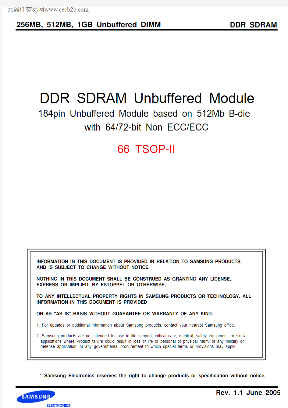

DDR SDRAM Unbuffered Module 184pin Unbuffered Module based on 512Mb B-die with 64/72-bit Non ECC/ECC
66 TSOP-II
INFORMATION IN THIS DOCUMENT IS PROVIDED IN RELATION TO SAMSUNG PRODUCTS, AND IS SUBJECT TO CHANGE WITHOUT NOTICE.
NOTHING IN THIS DOCUMENT SHALL BE CONSTRUED AS GRANTING ANY LICENSE, EXPRESS OR IMPLIED, BY ESTOPPEL OR OTHERWISE,
TO ANY INTELLECTUAL PROPERTY RIGHTS IN SAMSUNG PRODUCTS OR TECHNOLOGY. ALL INFORMATION IN THIS DOCUMENT IS PROVIDED
ON AS "AS IS" BASIS WITHOUT GUARANTEE OR WARRANTY OF ANY KIND.
1. For updates or additional information about Samsung products, contact your nearest Samsung office.
2. Samsung products are not intended for use in life support, critical care, medical, safety equipment, or similar applications where Product failure could result in loss of life or personal or physical harm, or any military or defense application, or any governmental procurement to which special terms or provisions may apply.
* Samsung Electronics reserves the right to change products or specification without notice.
Table of Contents
1.0 Ordering Information (4)
2.0 Operating Frequencies (4)
3.0 Feature (4)
4.0 Pin Configuration (Front side/back side) (5)
5.0 Pin Description (5)
6.0 Functional Block Diagram (6)
6.1 256MB, 32M x 64 Non ECC Module (M368L3324BT(U)) (6)
6.2 512MB, 64M x 64 Non ECC Module (M368L6523BT(U)) (7)
6.3 512MB, 64M x 72 ECC Module (M381L6523B(U)) (8)
6.4 1GB, 128M x 64 Non ECC Module (M368L2923BT(U)) (9)
6.5 1GB, 128M x 72 ECC Module (M381L2923BT(U)) (10)
7.0 Absolute Maximum Ratings (11)
8.0 DC Operating Conditions (11)
9.0 DDR SDRAM IDD spec table (12)
9.1 M368L3324BT(U) [ (32M x 16) * 4, 256MB Non ECC Module ] (12)
9.2 M368L6523BT(U) [ (64M x 8) * 8, 512MB Non ECC Module ] (12)
9.3 M381L6523BT(U) [ (64M x 8) * 9, 512MB ECC Module ] (13)
9.4 M368L2923BT(U) [ (64M x 8) * 16, 1GB Non ECC Module ] (13)
9.5 M381L2923BT(U) [ (64M x 8) * 18, 1GB ECC Module ] (14)
10.0 AC Operating Conditions (15)
11.0 Input/Output Capacitance (15)
12.0 AC Timming Parameters & Specifications (16)
13.0 System Characteristics for DDR SDRAM (17)
14.0 Component Notes (18)
15.0 System Notes (19)
16.0 Command Truth Table (20)
17.0 Physical Dimensions (21)
17.1 32M x 64 (M368L3324BT(U)) (21)
17.2 64Mx64 (M368L6523BT(U)) (22)
17.3 64Mx72 (M381L6523BT(U)) (23)
17.4 128Mx64 (M368L2923BT(U)) (24)
17.5 128Mx72 (M381L2923BT(U)) (25)
Revision History
Revision Month Year History
0.0February2003 - First version for internal review
1.0August2003 - Revision 1.0 spec release.
1.1June2005 - Deleted “B0, AA, A2” speed and changed master format.
CC(DDR400@CL=3)
B3(DDR333@CL=2.5)
Speed @CL2-133MHz Speed @CL2.5166MHz 166MHz
Speed @CL3200MHz -CL-tRCD-tRP
3-3-3
2.5-3-3
184Pin Unbuffered DIMM based on 512Mb B-die (x8, x16)
? VDD : 2.5V ± 0.2V, VDDQ : 2.5V ± 0.2V for DDR333 ? VDD : 2.6V ± 0.1V, VDDQ : 2.6V ± 0.1V for DDR400
? Double-data-rate architecture; two data transfers per clock cycle ? Bidirectional data strobe [DQ] (x4,x8) & [L(U)DQS] (x16) ? Differential clock inputs(CK and CK)
? DLL aligns DQ and DQS transition with CK transition
? Programmable Read latency : DDR333(2.5 Clock), DDR400(3 Clock)? Programmable Burst length (2, 4, 8)
? Programmable Burst type (sequential & interleave)? Edge aligned data output, center aligned data input
? Auto & Self refresh, 7.8us refresh interval(8K/64ms refresh) ? Serial presence detect with EEPROM
? PCB : Height 1,250 (mil) & single (256, 512MB), double (1GB) sided ? SSTL_2 Interface
? 66pin TSOP II (Leaded & Pb-Free(RoHS compliant)) package
1.0 Ordering Information
2.0 Operating Frequencies
Note : Leaded and Lead-free(Pb-free) can be discriminated by PKG P/N (T : 66 TSOP with Leaded, U : 66 TSOP with Lead-free)
Part Number
Density Organization Component Composition Height M368L3324BT(U)M-C(L)CC/B3256MB 32M x 64 32Mx16 (K4H511638B) * 4EA 1,250mil M368L6523BT(U)M-C(L)CC 512MB 64M x 64 64Mx8 (K4H510838B) * 8EA 1,250mil M368L6523BT(U)N-C(L)B3M381L6523BT(U)M-C(L)CC/B3512MB 64M x 72 64Mx8 (K4H510838B) * 9EA 1,250mil M368L2923BT(U)M-C(L)CC 1GB 128M x 64 64Mx8 (K4H510838B) * 16EA 1,250mil M368L2923BT(U)N-C(L)B3M381L2923BT(U)M-C(L)CC/B3
1GB
128M x 72
64Mx8 (K4H510838B) * 18EA
1,250mil
3.0 Feature
Note :
1. * : These pins are not used in this module.
2. Pins 44, 45, 47, 49, 51, 134, 135, 140, 142, 144 are used on x72 module ( M381~ ), and are not used on x64 module.
3. Pins 111, 158 are NC for 1row modules & used for 2row modules[ M368(81)L2923B ].
4. Pins 137, 138 are NC for x16 1Row module (M368L3324B).
Pin Front Pin Front Pin Front Pin Back Pin Back Pin Back 1VREF 32A562VDDQ 93VSS 124VSS 154RAS 2DQ033DQ2463WE 94DQ4125A6155DQ453VSS 34VSS 64DQ4195DQ5126DQ28156VDDQ 4DQ135DQ2565CAS 96VDDQ 127DQ29157CS05DQS036DQS366VSS 97DM0128VDDQ 158CS16DQ237A467DQS598DQ6129DM3159DM57VDD 38VDD 68DQ4299DQ7130A3160VSS 8DQ339DQ2669DQ43100VSS 131DQ30161DQ469NC 40DQ2770VDD 101NC 132VSS 162DQ4710NC 41A271*CS2102NC 133DQ31163*CS311VSS 42VSS 72DQ48103NC 134CB4164VDDQ 12DQ843A173DQ49104VDDQ 135CB5165DQ5213DQ944CB074VSS 105DQ12136VDDQ 166DQ5314DQS145CB175*CK2106DQ13137CK0167*A1315VDDQ 46VDD 76*CK2107DM1138CK0168VDD 16CK147DQS877VDDQ 108VDD 139VSS 169DM617CK148A078DQS6109DQ14140DM8170DQ5418VSS 49CB279DQ50110DQ15141A10171DQ5519DQ1050VSS 80DQ51111CKE1142CB6172VDDQ 20DQ1151CB381VSS 112VDDQ 143VDDQ 173NC 21CKE052BA182VDDID 113*BA2144CB7174DQ6022VDDQ KEY
83DQ56114DQ20KEY
175DQ6123DQ1653DQ3284DQ57115A12145VSS 176VSS 24DQ1754VDDQ 85VDD 116VSS 146DQ36177DM725DQS255DQ3386DQS7117DQ21147DQ37178DQ6226VSS 56DQS487DQ58118A11148VDD 179DQ6327A957DQ3488DQ59119DM2149DM4180VDDQ 28DQ1858VSS 89VSS 120VDD 150DQ38181SA029A759BA090NC 121DQ22151DQ39182SA130VDDQ 60DQ3591SDA 122A8152VSS 183SA231
DQ19
61
DQ40
92
SCL
123
DQ23
153
DQ44
184
VDDSPD
Note : VDDID defines relationship of VDD and VDDQ, and the default status of it is open (VDD=VDDQ)
Pin Name
Function
Pin Name Function A0 ~ A12Address input (Multiplexed)DM0 ~7,8(for ECC)Data - in mask
BA0 ~ BA1A Bank Select Address VDD
Power supply
(2.5V for DDR333, 2.6V for DDR400)DQ0 ~ DQ63
Data input/output
VDDQ
Power Supply for DQS
(2.5V for DDR333, 2.6V for DDR400)
DQS0 ~ DQS8
Data Strobe input/output VSS Ground CK0,CK0 ~ CK2, CK2
Clock input
VREF Power supply for reference CKE0, CKE1(for double banks)Clock enable input VDDSPD Serial EEPROM Power/Supply ( 2.3V to 3.6V )CS0, CS1(for double banks)Chip select input SDA Serial data I/O RAS Row address strobe SCL Serial clock CAS Column address strobe SA0 ~ 2Address in EEPROM WE
Write enable
VDDID VDD, VDDQ level detection CB0 ~ CB7(for x72 module)
Check bit(Data-in/data-out)
NC No connection
5.0 Pin Description
4.0 Pin Configuration (Front side/back side)
(Populated as 1 bank of x16 DDR SDRAM Module)
6.1 256MB, 32M x 64 Non ECC Module (M368L3324BT(U))
6.0 Functional Block Diagram
DM1
DQS1DM0
DQS0A0 - A12A0-A12: DDR SDRAMs D0 - D3BA0 - BA1BA0-BA1: DDR SDRAMs D0 - D3RAS RAS: DDR SDRAMs D0 - D3CAS CAS: DDR SDRAMs D0 - D3CKE: DDR SDRAMs D0 - D3 Clock Wiring CK0/CK0
Clock
Input DDR SDRAMs CK1/CK1NC
2 DDR SDRAMs 2 DDR SDRAMs
CK2/CK2
V SS
V DD /V VREF V SPD Notes:
1. DQ-to-I/O wiring is shown as recomended but may be changed.
2. DQ/DQS/DM/CKE/CS relationships must be maintained as shown.
3. DQ, DQS, DM/DQS resistors: 22 Ohms + 5%.
4. BAx, Ax, RAS, CAS, WE resistors: 7.5 Ohms + 5%
DM3
DQS3DM0
DQS0
(Populated as 1 bank of x8 DDR SDRAM Module)
6.2 512MB, 64M x 64 Non ECC Module (M368L6523BT(U))
CS0DQS0DM0
DM/
CS
DQS
DQ0DQ1DQ2DQ3DQ4DQ5DQ6DQ7
D0
DQS1DM1
DM/CS DQS DQ8DQ9DQ10DQ11DQ12DQ13DQ14DQ15
D1
DQS2DM2
DM/CS DQS
DQ16DQ17DQ18DQ19DQ20DQ21DQ22DQ23
D2
DQS3DM3
DM/CS DQS
DQ24DQ25DQ26DQ27DQ28DQ29DQ30DQ31D3
DQS4DM4
DM/
CS
DQS
DQ32DQ33DQ34DQ35DQ36DQ37DQ38DQ39
D4
DQS5DM5
DM/CS DQS
DQ40DQ41DQ42DQ43DQ44DQ45DQ46DQ47
D5
DQS6DM6
DM/
CS
DQS
DQ48DQ49DQ50DQ51DQ52DQ53DQ54DQ55
D6
DQS7DM7
DM/
CS
DQS
DQ56DQ57DQ58DQ59DQ60DQ61DQ62DQ63D7
I/O 6I/O 4I/O 2I/O 0I/O 7I/O 5I/O 3I/O 1
I/O 7I/O 5I/O 1I/O 0I/O 6I/O 4I/O 3I/O 2
I/O 6I/O 5I/O 3I/O 0I/O 7I/O 4I/O 2I/O 1
I/O 7I/O 4I/O 2I/O 1I/O 6I/O 5I/O 3I/O 0
I/O 7I/O 4I/O 1I/O 3I/O 6I/O 5I/O 0I/O 2
I/O 6I/O 4I/O 3I/O 1I/O 7I/O 5I/O 2I/O 0
I/O 7I/O 5I/O 1I/O 0I/O 6I/O 4I/O 3I/O 2
I/O 5I/O 4I/O 1I/O 0I/O 7I/O 6I/O 3I/O 2
A0 - A12
A0-A12 : DDR SDRAMs D0 - D7RAS RAS : DDR SDRAMs D0 - D7CAS CAS : DDR SDRAMs D0 - D7WE
WE : DDR SDRAMs D0 - D7
CKE0CKE : DDR SDRAMs D0 - D7BA0 - BA1BA0-BA1 : DDR SDRAMs D0 - D7V SS
D0 - D7
V DD /V DDQ
D0 - D7D0 - D7VREF V DDSPD SPD D0 - D7
*Clock Net Wiring
* Clock Wiring Clock Input DDR SDRAMs *CK0/CK0*CK1/CK1*CK2/CK2
2 DDR SDRAMs
3 DDR SDRAMs 3 DDR SDRAMs
Card
Edge
D3/D0/D5
Cap/Cap/Cap
Cap/D1/D6 Cap/Cap/Cap D4/D2/C7
Cap/Cap/Cap
R=120?
CK0/1/2
Notes :
1. DQ-to-I/O wiring is shown as recommended but may be changed.
maintained as shown.
3. DQ, DQS, DM/DQS resistors: 22 Ohms + 5%.
4. BAx, Ax, RAS, CAS, WE resistors:
5.1 Ohms + 5%
Cap
(Populated as 1 bank of x8 DDR SDRAM Module)
6.3 512MB, 64M x 72 ECC Module (M381L6523BT(U))
A0 - A12
A0-A12 : DDR SDRAMs D0 - D8RAS RAS : DDR SDRAMs D0 - D8CAS CAS : DDR SDRAMs D0 - D8WE
WE : DDR SDRAMs D0 - D8
CKE0CKE : DDR SDRAMs D0 - D8BA0 - BA1BA0-BA1 : DDR SDRAMs D0 - D8V SS
D0 - D8
V DD /V DDQ
D0 - D8D0 - D8VREF V DDSPD SPD D0 - D8
*Clock Net Wiring
* Clock Wiring Clock Input DDR SDRAMs *CK0/CK0*CK1/CK1*CK2/CK2
3 DDR SDRAMs 3 DDR SDRAMs 3 DDR SDRAMs
CS0DQS0DM0
DM/
CS
DQS
DQ0DQ1DQ2DQ3DQ4DQ5DQ6DQ7
D0
DQS1DM1
DM/CS DQS DQ8DQ9DQ10DQ11DQ12DQ13DQ14DQ15
D1
DQS2DM2
DM/CS DQS
DQ16DQ17DQ18DQ19DQ20DQ21DQ22DQ23
D2
DQS3DM3
DM/CS DQS DQ24DQ25DQ26DQ27DQ28DQ29DQ30DQ31
D3
DQS4DM4
DM/
CS
DQS
DQ32DQ33DQ34DQ35DQ36DQ37DQ38DQ39
D4
DQS5DM5
DM/CS DQS
DQ40DQ41DQ42DQ43DQ44DQ45DQ46DQ47
D5
DQS6DM6
DM/
CS
DQS
DQ48DQ49DQ50DQ51DQ52DQ53DQ54DQ55
D6
DQS7DM7
DM/CS DQS
DQ56DQ57DQ58DQ59DQ60DQ61DQ62DQ63D7
I/O 6I/O 4I/O 2I/O 0I/O 7I/O 5I/O 3I/O 1
I/O 7I/O 5I/O 1I/O 0I/O 6I/O 4I/O 3I/O 2
I/O 6I/O 5I/O 3I/O 0I/O 7I/O 4I/O 2I/O 1
I/O 7I/O 4I/O 3I/O 1I/O 6I/O 5I/O 2I/O 0
I/O 7I/O 4I/O 3I/O 0I/O 6I/O 5I/O 2I/O 1
I/O 6I/O 4I/O 3I/O 2I/O 7I/O 5I/O 1I/O 0
I/O 7I/O 6I/O 1I/O 0I/O 5I/O 4I/O 3I/O 2
I/O 5I/O 4I/O 1I/O 0I/O 7I/O 6I/O 3I/O 2
DQS8DM8
DM/CS DQS
CB0CB1CB2CB3CB4CB5CB6CB7D8
I/O 5I/O 4I/O 3I/O 1I/O 7I/O 6I/O 2I/O 0
Card
Edge
D3/D0/D6
Cap/Cap/Cap
D4/D1/D7 Cap/Cap/Cap D5/D2/D8Cap/Cap/Cap
R=120?
CK0/1/2
Notes :
1. DQ-to-I/O wiring is shown as recommended but may be changed.
2. DQ/DQS/DM/CKE/CS relationships must be maintained as shown.
3. DQ, DQS, DM/DQS resistors: 22 Ohms + 5%.
4. BAx, Ax, RAS, CAS, WE resistors:
5.1 Ohms + 5%
(Populated as 2 bank of x8 DDR SDRAM Module)
6.4 1GB, 128M x 64 Non ECC Module (M368L2923BT(U))
CS0
DQS0
DM0
DM/CS DQS
DQ0
DQ1
DQ2
DQ3
DQ4
DQ5
DQ6
DQ7
D0
DQS1
DM1
DM/CS DQS
DQ8
DQ9
DQ10
DQ11
DQ12
DQ13
DQ14
DQ15
D1
DQS2
DM2
DM/CS DQS
DQ16
DQ17
DQ18
DQ19
DQ20
DQ21
DQ22
DQ23
D2
DQS3
DM3
DM/CS DQS
DQ24
DQ25 DQ26 DQ27 DQ28 DQ29 DQ30 DQ31D3
DQS4
DM4
DM/CS DQS
DQ32
DQ33
DQ34
DQ35
DQ36
DQ37
DQ38
DQ39
D4
DQS5
DM5
DM/CS DQS
DQ40
DQ41
DQ42
DQ43
DQ44
DQ45
DQ46
DQ47
D5
DQS6
DM6
DM/CS DQS
DQ48
DQ49
DQ50
DQ51
DQ52
DQ53
DQ54
DQ55
D6
DQS7
DM7
DM/CS DQS
DQ56
DQ57
DQ58
DQ59
DQ60
DQ61
DQ62
DQ63
D7
I/O 7
I/O 6
I/O 1
I/O 0
I/O 5
I/O 4
I/O 3
I/O 2
I/O 5
I/O 6
I/O 1
I/O 0
I/O 7
I/O 4
I/O 3
I/O 2
I/O 5
I/O 4
I/O 1
I/O 0
I/O 7
I/O 6
I/O 3
I/O 2
I/O 5
I/O 6
I/O 1
I/O 0
I/O 7
I/O 4
I/O 3
I/O 2
I/O 7
I/O 6
I/O 1
I/O 2
I/O 5
I/O 4
I/O 3
I/O 0
I/O 7
I/O 6
I/O 1
I/O 0
I/O 5
I/O 4
I/O 3
I/O 2
I/O 7
I/O 6
I/O 1
I/O 2
I/O 5
I/O 4
I/O 3
I/O 0
I/O 7
I/O 6
I/O 1
I/O 0
I/O 5
I/O 4
I/O 3
I/O 2
DM/CS DQS
D8
DM/CS DQS
D9
DM/CS DQS
D10
DM/CS DQS
D11
I/O 0
I/O 1
I/O 6
I/O 7
I/O 2
I/O 3
I/O 4
I/O 5
DM/CS DQS
D12
DM/CS DQS
D13
DM/CS DQS
D14
DM/CS DQS
D15
CS1
I/O 2
I/O 1
I/O 6
I/O 7
I/O 0
I/O 3
I/O 4
I/O 5
I/O 2
I/O 3
I/O 6
I/O 7
I/O 0
I/O 1
I/O 4
I/O 5
I/O 2
I/O 1
I/O 6
I/O 7
I/O 0
I/O 3
I/O 4
I/O 5
I/O 0
I/O 1
I/O 6
I/O 5
I/O 2
I/O 3
I/O 4
I/O 7
I/O 0
I/O 1
I/O 6
I/O 7
I/O 2
I/O 3
I/O 4
I/O 5
I/O 0
I/O 1
I/O 6
I/O 5
I/O 2
I/O 3
I/O 4
I/O 7
I/O 0
I/O 1
I/O 6
I/O 7
I/O 2
I/O 3
I/O 4
I/O 5
A0 - A12A0-A12: DDR SDRAMs D0 - D15
BA0 - BA1BA0-BA1 : DDR SDRAMs D0 - D15
V SS D0 - D15
V DD/V DDQ D0 - D15
D0 - D15
VREF
V DDSPD SPD
D0 - D15
*Clock Net Wiring
* Clock Wiring
Clock
Input
DDR SDRAMs
*CK0/CK0
*CK1/CK1
*CK2/CK2
4 DDR SDRAMs
6 DDR SDRAMs
6 DDR SDRAMs
Card
Edge
D3/D0/D5
D11/D8/D13
Cap/D1/D6
Cap/D9/D14
D4/D2/D7
D12/D10/D15
R=120?
CK0/1/2
*
*
CKE 0/1CKE : DDR SDRAMs D0 - D15
CK0/1/2
Notes :
1. DQ-to-I/O wiring is shown as recommended
but may be changed.
maintained as shown.
3. DQ, DQS, DM/DQS resistors: 22 Ohms + 5%.
4. BAx, Ax, RAS, CAS, WE resistors: 3 Ohms +
5%
(Populated as 2 bank of x8 DDR SDRAM Module)
6.5 1GB, 128M x 72 ECC Module (M381L2923BT(U))
CS0DQS0DM0
DM/
CS
DQS
DQ0DQ1DQ2DQ3DQ4DQ5DQ6DQ7
D0
DQS1DM1
DM/CS DQS DQ8DQ9DQ10DQ11DQ12DQ13DQ14DQ15
D1
DQS2DM2
DM/CS DQS DQ16DQ17DQ18DQ19DQ20DQ21DQ22DQ23
D2
DQS3DM3
DM/CS DQS DQ24DQ25DQ26DQ27DQ28DQ29DQ30DQ31
D3
DQS4DM4
DM/
CS
DQS
DQ32DQ33DQ34DQ35DQ36DQ37DQ38DQ39
D4
DQS5DM5
DM/CS DQS DQ40DQ41DQ42DQ43DQ44DQ45DQ46DQ47
D5
DQS6DM6
DM/CS DQS DQ48DQ49DQ50DQ51DQ52DQ53DQ54DQ55
D6
DQS7DM7
DM/CS DQS DQ56DQ57DQ58DQ59DQ60DQ61DQ62DQ63D7
I/O 7I/O 6I/O 1I/O 0I/O 5I/O 4I/O 3I/O 2
I/O 7I/O 6I/O 1I/O 0I/O 5I/O 4I/O 3I/O 2
I/O 7I/O 6I/O 1I/O 0I/O 5I/O 4I/O 3I/O 2
I/O 7I/O 6I/O 1I/O 0I/O 5I/O 4I/O 3I/O 2
I/O 7I/O 6I/O 1I/O 0I/O 5I/O 4I/O 3I/O 2
I/O 7I/O 6I/O 1I/O 0I/O 5I/O 4I/O 3I/O 2
I/O 7I/O 6I/O 1I/O 0I/O 5I/O 4I/O 3I/O 2
I/O 7I/O 6I/O 1I/O 0I/O 5I/O 4I/O 3I/O 2
DM/
CS
DQS
D9
DM/CS DQS D10
DM/CS DQS D11
DM/CS DQS D12
I/O 0I/O 1I/O 6I/O 7I/O 2I/O 3I/O 4I/O 5
DM/
CS
DQS
D13
DM/CS DQS
D14
DM/CS DQS
D15
DM/CS DQS
D16
CS1I/O 0I/O 1I/O 6I/O 7I/O 2I/O 3I/O 4I/O 5
I/O 0I/O 1I/O 6I/O 7I/O 2I/O 3I/O 4I/O 5
I/O 0I/O 1I/O 6I/O 7I/O 2I/O 3I/O 4I/O 5
I/O 0I/O 1I/O 6I/O 7I/O 2I/O 3I/O 4I/O 5
I/O 0I/O 1I/O 6I/O 7I/O 2I/O 3I/O 4I/O 5
I/O 0I/O 1I/O 6I/O 7I/O 2I/O 3I/O 4I/O 5
I/O 0I/O 1I/O 6I/O 7I/O 2I/O 3I/O 4I/O 5
A0 - A12
A0-A12 : DDR SDRAMs D0 - D17RAS RAS : DDR SDRAMs D0 - D17WE
WE : DDR SDRAMs D0 - D17
BA0 - BA1BA0-BA1 : DDR SDRAMs D0 - D17V SS
D0 - D17
V DD /V DDQ
D0 - D17D0 - D17VREF V DDSPD
SPD D0 - D17
*Clock Net Wiring
* Clock Wiring Clock Input DDR SDRAMs *CK0/CK0*CK1/CK1*CK2/CK2
6 DDR SDRAMs 6 DDR SDRAMs 6 DDR SDRAMs
A0Serial PD
A1A2SA0
SA1
SA2
SCL SDA
WP
Card Edge
D3/D0/D5D12/D9/D14
D8/D1/D6 D17/D10/D15D4/D2/D7D13/D11/D16
R=120?
CK0/1/2
CKE0/1
CKE : DDR SDRAMs D0 - D17DQS8DM8
DM/CS DQS D8
I/O 7I/O 6I/O 1I/O 0I/O 5I/O 4I/O 3I/O 2
DM/CS DQS
D17
I/O 0I/O 1I/O 6I/O 7I/O 2I/O 3I/O 4I/O 5
CB0CB1CB2CB3CB4CB5CB6CB7Notes :
1. DQ-to-I/O wiring is shown as recommended but may be changed.
2. DQ/DQS/DM/CKE/CS relationships must be maintained as shown.
3. DQ, DQS, DM/DQS resistors: 22 Ohms + 5%.
4. BAx, Ax, RAS, CAS, WE resistors:3 Ohms + 5%
7.0 Absolute Maximum Ratings
Parameter Symbol Value Unit Voltage on any pin relative to V SS V IN,V OUT-0.5 ~ 3.6V Voltage on V DD & V DDQ supply relative to V SS V DD,V DDQ-1.0 ~ 3.6V Storage temperature T STG-55 ~ +150°C Power dissipation P D 1.5 * # of component W
Short circuit current I OS50mA
Note :
Permanent device damage may occur if ABSOLUTE MAXIMUM RATINGS are exceeded.
Functional operation should be restricted to recommended operating condition.
Exposure to higher than recommended voltage for extended periods of time could affect device reliability.
8.0 DC Operating Conditions
Recommended operating conditions(Voltage referenced to V SS=0V, T A=0 to 70°C)
Parameter Symbol Min Max Unit Note Supply voltage(for device with a nominal V DD of 2.5V for DDR333)V DD 2.3 2.7V
Supply voltage(for device with a nominal V DD of 2.6V for DDR400)V DD 2.5 2.7V
I/O Supply voltage(for device with a nominal V DD of 2.5V for DDR333)V DDQ 2.3 2.7V
I/O Supply voltage(for device with a nominal V DD of 2.6V for DDR400)V DDQ 2.5 2.7V
I/O Reference voltage V REF0.49*VDDQ0.51*VDDQ V1
I/O Termination voltage(system)V TT V REF-0.04V REF+0.04V2 Input logic high voltage V IH(DC)V REF+0.15V DDQ+0.3V
Input logic low voltage V IL(DC)-0.3V REF-0.15V
Input Voltage Level, CK and CK inputs V IN(DC)-0.3V DDQ+0.3V
Input Differential Voltage, CK and CK inputs V ID(DC)0.36V DDQ+0.6V3
V-I Matching: Pullup to Pulldown Current Ratio VI(Ratio)0.71 1.4-4 Input leakage current I I-22uA
Output leakage current I OZ-55uA
Output High Current(Normal strengh driver) ;V OUT = V TT + 0.84V I OH-16.8mA
Output High Current(Normal strengh driver) ;V OUT = V TT - 0.84V I OL16.8mA
Output High Current(Half strengh driver) ;V OUT = V TT + 0.45V I OH-9mA
Output High Current(Half strengh driver) ;V OUT = V TT - 0.45V I OL9mA
Note :
1. V REF is expected to be equal to 0.5*V DDQ of the transmitting device, and to track variations in the dc level of same. Peak-to peak noise on V REF may
not exceed +/-2% of the dc value.
2. V TT is not applied directly to the device. V TT is a system supply for signal termination resistors, is expected to be set equal to V REF, and must track
variations in the DC level of V REF.
3. V ID is the magnitude of the difference between the input level on CK and the input level on CK.
4. The ratio of the pullup current to the pulldown current is specified for the same temperature and voltage, over the entire temperature and voltage range,
for device drain to source voltages from 0.25V to 1.0V. For a given output, it represents the maximum difference between pullup and pulldown drivers due to process variation. The full variation in the ratio of the maximum to minimum pullup and pulldown current will not exceed 1.7 for device drain to source voltages from 0.1 to 1.0.
(V DD =2.7V, T = 10°C)
* Module IDD was calculated on the basis of component IDD and can be differently measured according to DQ loading cap.
Symbol CC(DDR400@CL=3)
B3(DDR333@CL=2.5)
Unit Notes
IDD0660500mA IDD1760620mA IDD2P 2020mA IDD2F 120120mA IDD2Q 100100mA IDD3P 220120mA IDD3N 400200mA IDD4R 920780mA IDD4W 1,120860mA IDD5
1,0601,000mA IDD6
Normal 2020mA Low power 1212mA Optional IDD7A
1,800
1,620
mA
(V DD =2.7V, T = 10°C)
* Module IDD was calculated on the basis of component IDD and can be differently measured according to DQ loading cap.
Symbol CC(DDR400@CL=3)
B3(DDR333@CL=2.5)
Unit Notes
IDD01,3201,000mA IDD11,4801,200mA IDD2P 4040mA IDD2F 240240mA IDD2Q 200200mA IDD3P 440240mA IDD3N 760400mA IDD4R 1,6001,320mA IDD4W 1,9201,520mA IDD5
2,1202,000mA IDD6
Normal 4040mA Low power 2424mA Optional IDD7A
3,440
3,200
mA
9.1 M368L3324BT(U) [ (32M x 16) * 4, 256MB Non ECC Module ]
9.2 M368L6523BT(U) [ (64M x 8) * 8, 512MB Non ECC Module ]
9.0 DDR SDRAM IDD spec table
(V DD =2.7V, T = 10°C)
* Module IDD was calculated on the basis of component IDD and can be differently measured according to DQ loading cap.
Symbol CC(DDR400@CL=3)
B0(DDR333@CL=2.5)
Unit Notes
IDD01,4851,130mA IDD11,6651,350mA IDD2P 4545mA IDD2F 270270mA IDD2Q 225230mA IDD3P 500270mA IDD3N 855450mA IDD4R 1,8001,490mA IDD4W 2,1601,710mA IDD5
2,3852,250mA IDD6
Normal 4545mA Low power 2727mA Optional IDD7A
3,870
3,600
mA
(V DD =2.7V, T = 10°C)
* Module IDD was calculated on the basis of component IDD and can be differently measured according to DQ loading cap.
Symbol CC(DDR400@CL=3)
B0(DDR333@CL=2.5)
Unit Notes
IDD02,0801,400mA IDD12,2401,600mA IDD2P 8080mA IDD2F 480480mA IDD2Q 400400mA IDD3P 880480mA IDD3N 1,520800mA IDD4R 2,3601,720mA IDD4W 2,6801,920mA IDD5
2,8802,400mA IDD6
Normal 8080mA Low power 4848mA Optional IDD7A
4,200
3,600
mA
9.4 M368L2923BT(U) [ (64M x 8) * 16, 1GB Non ECC Module ]
9.3 M381L6523BT(U) [ (64M x 8) * 9, 512MB ECC Module ]
(V DD =2.7V, T = 10°C)
* Module IDD was calculated on the basis of component IDD and can be differently measured according to DQ loading cap.
Symbol CC (DDR400@CL=3)
B3 (DDR333@CL=2.5)
Unit Notes
IDD02,3401,580mA IDD12,5201,800mA IDD2P 9090mA IDD2F 540540mA IDD2Q 450450mA IDD3P 990540mA IDD3N 1,710900mA IDD4R 2,6551,940mA IDD4W 3,0152,160mA IDD5
3,2402,700mA IDD6
Normal 9090mA Low power 5454mA Optional IDD7A
4,725
4,050
mA
9.5 M381L2923BT(U) [ (64M x 8) * 18, 1GB ECC Module ]
Output Load Circuit (SSTL_2)
Output
Z0=50?C LOAD =30pF
V REF
=0.5*V DDQ
R T =50?
V tt =0.5*V DDQ
(VDD=2.5V, VDDQ=2.5V, TA= 25°C, f=1MHz)
Parameter
Symbol M368L3324BT(U)M368L6523BT(U)M381L6523BT(U)Unit Min Max Min Max Min Max Input capacitance(A0 ~ A12, BA0 ~ BA1,RAS,CAS,WE
)CIN1414549575160pF Input capacitance(CKE0)CIN2343842504453pF Input capacitance( CS0)
CIN3343842504453pF Input capacitance( CLK0, CLK1,CLK2)CIN4253025302530pF Input capacitance(DM0~DM7, DM8(for
ECC))CIN5676767pF Data & DQS input/output
capacitance(DQ0~DQ63)Cout1676767pF Data input/output capacitance (CB0~CB7)Cout2
----6
7
pF
Parameter
Symbol M368L2923BT(U)M381L2923BT(U)Unit Min Max Min Max Input capacitance(A0 ~ A12, BA0 ~ BA1,RAS,CAS,WE )CIN165816987pF Input capacitance(CKE0,CKE1)CIN242504453pF Input capacitance( CS0, CS1)CIN342504453pF Input capacitance( CLK0, CLK1,CLK2)CIN428342834pF Input capacitance(DM0~DM7, DM8(for ECC))CIN510121012pF Data & DQS input/output capacitance(DQ0~DQ63)Cout110121012pF Data input/output capacitance (CB0~CB7)
Cout2
--10
12
pF
Note :
1. VID is the magnitude of the difference between the input level on CK and the input on CK.
2. The value of V IX is expected to equal 0.5*V DDQ of the transmitting device and must track variations in the DC level of the same.
3. These parameters should be tested at the pim on actual components and may be checked at either the pin or the pad in simulation. the AC and DC input specificatims are refation to a Vref envelope that has been bandwidth limited 20MHz.
Parameter/Condition
Symbol Min Max
Unit Note Input High (Logic 1) Voltage, DQ, DQS and DM signals VIH(AC)VREF + 0.31
V 3Input Low (Logic 0) Voltage, DQ, DQS and DM signals.
VIL(AC)VREF - 0.31V 3Input Differential Voltage, CK and CK inputs VID(AC)0.7VDDQ+0.6V 1Input Crossing Point Voltage, CK and CK inputs
VIX(AC)
0.5*VDDQ-0.2
0.5*VDDQ+0.2
V
2
11.0 Input/Output Capacitance
10.0 AC Operating Conditions
Parameter Symbol
CC
(DDR400@CL=3.0)
B3
(DDR333@CL=2.5)Unit Note Min Max Min Max
Row cycle time tRC5560ns Refresh row cycle time tRFC7072ns Row active time tRAS4070K4270K ns RAS to CAS delay tRCD1518ns Row precharge time tRP1518ns Row active to Row active delay tRRD1012ns Write recovery time tWR1515ns Last data in to Read command tWTR21tCK
Clock cycle time CL=2.0
tCK
--7.512ns CL=2.5612612ns CL=3.0510--
Clock high level width tCH0.450.550.450.55tCK
Clock low level width tCL0.450.550.450.55tCK
DQS-out access time from CK/CK tDQSCK-0.55+0.55-0.6+0.6ns
Output data access time from CK/CK tAC-0.65+0.65-0.7+0.7ns
Data strobe edge to ouput data edge tDQSQ-0.4-0.45ns22 Read Preamble tRPRE0.9 1.10.9 1.1tCK
Read Postamble tRPST0.40.60.40.6tCK
CK to valid DQS-in tDQSS0.72 1.280.75 1.25tCK
DQS-in setup time tWPRES00ns13 DQS-in hold time tWPRE0.250.25tCK
DQS falling edge to CK rising-setup time tDSS0.20.2tCK
DQS falling edge from CK rising-hold time tDSH0.20.2tCK
DQS-in high level width tDQSH0.35 0.35 tCK
DQS-in low level width tDQSL0.35 0.35 tCK
Address and Control Input setup time(fast)tIS0.60.75ns15, 17~19 Address and Control Input hold time(fast)tIH0.60.75ns15, 17~19 Address and Control Input setup time(slow)tIS0.70.8ns16~19 Address and Control Input hold time(slow)tIH0.70.8ns16~19 Data-out high impedence time from CK/CK tHZ-0.65+0.65-0.7+0.7ns11 Data-out low impedence time from CK/CK tLZ-0.65+0.65-0.7+0.7ns11 Mode register set cycle time tMRD1012ns
DQ & DM setup time to DQS tDS0.40.45ns j, k DQ & DM hold time to DQS tDH0.40.45ns j, k Control & Address input pulse width tIPW 2.2 2.2ns18 DQ & DM input pulse width tDIPW 1.75 1.75ns18 Exit self refresh to non-Read command tXSNR7575ns
Exit self refresh to read command tXSRD200200tCK
Refresh interval time tREFI7.87.8us14
Output DQS valid window tQH
tHP
-tQHS
-
tHP
-tQHS
-ns21
Clock half period tHP
tCLmin
or tCHmin
-
tCLmin
or tCHmin
-ns20, 21
Data hold skew factor tQHS0.50.55ns21 DQS write postamble time tWPST0.40.60.40.6tCK12 Active to Read with Auto precharge
command
tRAP15 18
Autoprecharge write recovery + Precharge time tDAL
(tWR/tCK)
+
(tRP/tCK)
(tWR/tCK)
+
(tRP/tCK)
tCK23
12.0 AC Timming Parameters & Specifications
The following specification parameters are required in systems using DDR333 devices to ensure proper system performance. these characteristics are for system simulation purposes and are guaranteed by design.Table 1 : Input Slew Rate for DQ, DQS, and DM
Table 2 : Input Setup & Hold Time Derating for Slew Rate
Table 3 : Input/Output Setup & Hold Time Derating for Slew Rate
Table 4 : Input/Output Setup & Hold Derating for Rise/Fall Delta Slew Rate
Table 5 : Output Slew Rate Characteristice (X4, X8 Devices only)
Table 6 : Output Slew Rate Characteristice (X16 Devices only)
Table 7 : Output Slew Rate Matching Ratio Characteristics
AC CHARACTERISTICS
DDR400DDR333PARAMETER
SYMBOL MIN MAX MIN MAX Units Notes DQ/DM/DQS input slew rate measured between VIH(DC), VIL(DC) and VIL(DC), VIH(DC)
DCSLEW
TBD
TBD
TBD
TBD
V/ns
a, m
Input Slew Rate
?tIS ?tIH Units Notes 0.5 V/ns 00ps i 0.4 V/ns +500ps i 0.3 V/ns
+100
ps
i
Input Slew Rate
?tDS ?tDH Units Notes 0.5 V/ns 00ps k 0.4 V/ns +75+75ps k 0.3 V/ns
+150
+150
ps
k
Delta Slew Rate ?tDS ?tDH Units Notes +/- 0.0 V/ns 00ps j +/- 0.25 V/ns +50+50ps j +/- 0.5 V/ns
+100
+100
ps
j
Slew Rate Characteristic
Typical Range
(V/ns)Minimum (V/ns)Maximum (V/ns)
Notes Pullup Slew Rate 1.2 ~ 2.5 1.0 4.5a,c,d,f,g,h Pulldown slew
1.2 ~
2.5
1.0
4.5
b,c,d,f,g,h
Slew Rate Characteristic
Typical Range
(V/ns)Minimum (V/ns)Maximum (V/ns)
Notes Pullup Slew Rate 1.2 ~ 2.50.7 5.0a,c,d,f,g,h Pulldown slew
1.2 ~
2.5
0.7
5.0
b,c,d,f,g,h
AC CHARACTERISTICS
DDR400DDR333PARAMETER
MIN MAX MIN MAX Notes Output Slew Rate Matching Ratio (Pullup to Pulldown)
TBD
TBD
TBD
TBD
e,m
13.0 System Characteristics for DDR SDRAM
1. All voltages referenced to Vss.
2. Tests for ac timing, IDD, and electrical, ac and dc characteristics, may be conducted at nominal reference/supply voltage levels, but the related speci-fications and device operation are guaranteed for the full voltage range specified.
3. Figure 1 represents the timing reference load used in defining the relevant timing parameters of the part. It is not intended to be either a precise rep-resentation of the typical system environment nor a depiction of the actual load presented by a production tester. System designers will use IBIS or other simulation tools to correlate the timing reference load to a system environment. Manufacturers will correlate to their production test conditions (generally a coaxial transmission line terminated at the tester electronics).
4. AC timing and IDD tests may use a VIL to VIH swing of up to 1.5 V in the test environment, but input timing is still referenced to VREF (or to the cross-ing point for CK/CK), and parameter specifications are guaranteed for the specified ac input levels under normal use conditions. The minimum slew rate for the input signals is 1 V/ns in the range between VIL(ac) and VIH(ac).
5. The ac and dc input level specifications are as defined in the SSTL_2 Standard (i.e., the receiver will effectively switch as a result of the signal crossing the ac input level and will remain in that state as long as the signal does not ring back above (below) the dc input LOW (HIGH) level.
6. Inputs are not recognized as valid until VREF stabilizes. Exception: during the period before VREF stabilizes, CKE ≤ 0.2VDDQ is recognized as LOW.
7. Enables on.chip refresh and address counters.
8. IDD specifications are tested after the device is properly initialized.
9. The CK/CK input reference level (for timing referenced to CK/CK) is the point at which CK and CK cross; the input reference level for signals other than CK/CK, is VREF.
10. The output timing reference voltage level is VTT.
11. tHZ and tLZ transitions occur in the same access time windows as valid data transitions. These parameters are not referenced to a specific voltage level but specify when the device output is no longer driving (HZ), or begins driving (LZ).
12. The maximum limit for this parameter is not a device limit. The device will operate with a greater value for this parameter, but sys tem performance (bus turnaround) will degrade accordingly.
13. The specific requirement is that DQS be valid (HIGH, LOW, or at some point on a valid transition) on or before this CK edge. A valid transition is defined as monotonic and meeting the input slew rate specifications of the device. when no writes were previ ously in progress on the bus, DQS will be tran sitioning from High- Z to logic LOW. If a previous write was in progress, DQS could be HIGH, LOW, or transitioning from HIGH to LOW at this time, depending on tDQSS.
14. A maximum of eight AUTO REFRESH commands can be posted to any given DDR SDRAM device.15. For command/address input slew rate ≥ 1.0 V/ns
16. For command/address input slew rate ≥ 0.5 V/ns and < 1.0 V/ns 17. For CK & CK slew rate ≥ 1.0 V/ns
18. These parameters guarantee device timing, but they are not necessarily tested on each device. They may be guaranteed by device design or tester correlation.
19. Slew Rate is measured between VOH(ac) and VOL(ac).
20. Min (tCL, tCH) refers to the smaller of the actual clock low time and the actual clock high time as provided to the device (i.e. this value can be greater than the minimum specification limits for tCL and tCH).....For example, tCL and tCH are = 50% of the period, less the half period jitter (tJIT(HP)) of the clock source, and less the half period jitter due to crosstalk (tJIT(crosstalk)) into the clock traces.21. tQH = tHP - tQHS, where:
tHP = minimum half clock period for any given cycle and is defined by clock high or clock low (tCH, tCL). tQHS accounts for 1) The pulse duration dis-tortion of on-chip clock circuits; and 2) The worst case push-out of DQS on one tansition followed by the worst case pull-in of DQ on the next transi-tion, both of which are, separately, due to data pin skew and output pattern effects, and p channel to n-channel variation of the output drivers.22. tDQSQ - Consists of data pin skew and output pattern effects, and p-channel to n-channel variation of the output drivers for any given cycle.23. tDAL = (tWR/tCK) + (tRP/tCK)
For each of the terms above, if not already an integer, round to the next highest integer. Example: For DDR266B at CL=2.5 and tCK=7.5ns tDAL = (15 ns / 7.5 ns) + (20 ns/ 7.5ns) = (2) + (3) tDAL = 5 clocks
Output VDDQ
50?
30pF
(Vout)
Figure 1 : Timing Reference Load
14.0 Component Notes
b. Pulldown slew rate is measured under the test conditions shown in Figure 3.
Output
Test point
VDDQ
50?
Figure 3 : Pulldown slew rate test load
c. Pullup slew rate is measured between (VDDQ/2 - 320 mV +/- 250 mV) Pulldown slew rate is measured between (VDDQ/2 + 320 mV +/- 250 mV)
Pullup and Pulldown slew rate conditions are to be met for any pattern of data, including all outputs switching and only one output switching. Example : For typical slew rate, DQ0 is switching For minmum slew rate, all DQ bits are switching from either high to low, or low to high.
The remaining DQ bits remain the same as for previous state.d. Evaluation conditions
Typical : 25 °C (T Ambient), VDDQ = 2.5V(for DDR266/333) and 2.6V(for DDR400), typical process
Minimum : 70 °C (T Ambient), VDDQ = 2.3V(for DDR266/333) and 2.5V(for DDR400), slow - slow process Maximum : 0 °C (T Ambient), VDDQ = 2.7V(for DDR266/333) and 2.7V(for DDR400), fast - fast process
e. The ratio of pullup slew rate to pulldown slew rate is specified for the same temperature and voltage, over the entire temperature and voltage range. For a given output, it represents the maximum difference between pullup and pulldown drivers due to process variation.
f. Verified under typical conditions for qualification purposes.
g. TSOPII package divices only.
h. Only intended for operation up to 266 Mbps per pin.
i. A derating factor will be used to increase tIS and tIH in the case where the input slew rate is below 0.5V/ns as shown in Table 2. The Input slew rate is based on the lesser of the slew rates detemined by either VIH(AC) to VIL(AC) or VIH(DC) to VIL(DC), similarly for rising transitions.j. A derating factor will be used to increase tDS and tDH in the case where DQ, DM, and DQS slew rates differ, as shown in Tables 3 & 4. Input slew rate is based on the larger of AC-AC delta rise, fall rate and DC-DC delta rise, Input slew rate is based on the lesser of the slew rates determined by either VIH(AC) to VIL(AC) or VIH(DC) to VIL(DC), similarly for rising transitions. The delta rise/fall rate is calculated as: {1/(Slew Rate1)} - {1/(Slew Rate2)} For example : If Slew Rate 1 is 0.5 V/ns and slew Rate 2 is 0.4 V/ns, then the delta rise, fall rate is - 0.5ns/V . Using the table given, this would result in the need for an increase in tDS and tDH of 100 ps.
k. Table 3 is used to increase tDS and tDH in the case where the I/O slew rate is below 0.5 V/ns. The I/O slew rate is based on the lesser on the lesser of the AC - AC slew rate and the DC- DC slew rate. The inut slew rate is based on the lesser of the slew rates deter mined by either VIH(ac) to VIL(ac) or VIH(DC) to VIL(DC), and similarly for rising transitions.m. DQS, DM, and DQ input slew rate is specified to prevent double clocking of data and preserve setup and hold times. Signal transi tions through the DC region must be monotonic.
a. Pullup slew rate is characteristized under the test conditions as shown in Figure 2.
Output
Test point
VSSQ
50?Figure 2 : Pullup slew rate test load
15.0 System Notes:
(V=Valid, X=Don ′t Care, H=Logic High, L=Logic Low)
Note :
1. OP Code : Operand Code. A 0 ~ A 12 & BA 0 ~ BA 1 : Program keys. (@EMRS/MRS)
2. EMRS/ MRS can be issued only at all banks precharge state. A new command can be issued 2 clock cycles after EMRS or MRS.
3. Auto refresh functions are same as the CBR refresh of DRAM.
The automatical precharge without row precharge command is meant by "Auto". Auto/self refresh can be issued only at all banks precharge state.4. BA 0 ~ BA 1 : Bank select addresses.
If both BA 0 and BA 1 are "Low" at read, write, row active and precharge, bank A is selected. If BA 0 is "High" and BA 1 is "Low" at read, write, row active and precharge, bank B is selected. If BA 0 is "Low" and BA 1 is "High" at read, write, row active and precharge, bank C is selected. If both BA 0 and BA 1 are "High" at read, write, row active and precharge, bank D is selected.5. If A 10/AP is "High" at row precharge, BA 0 and BA 1 are ignored and all banks are selected.6. During burst write with auto precharge, new read/write command can not be issued. Another bank read/write command can be issued after the end of burst.
New row active of the associated bank can be issued at t RP after the end of burst.7. Burst stop command is valid at every burst length.
8. DM sampled at the rising and falling edges of the DQS and Data-in are masked at the both edges (Write DM latency is 0). 9. This combination is not defined for any function, which means "No Operation(NOP)" in DDR SDRAM.
COMMAND
CKEn-1CKEn CS RAS CAS WE BA0,1A10/AP A0 ~ A9A11, A12
Note Register Extended MRS H X L L L L OP CODE 1, 2Register
Mode Register Set H X L L L L OP CODE
1, 2Refresh
Auto Refresh
H H L L L H X 3Self
Refresh
Entry L 3Exit
L H L H H H X
3H X X X 3
Bank Active & Row Addr.
H X L L H H V Row Address (A0~A9, A11,A12)Read &
Column Address Auto Precharge Disable H X L H L H V L Column Address 4Auto Precharge Enable H 4Write &
Column Address
Auto Precharge Disable H X L H L L V
L Column Address
4Auto Precharge Enable
H 4, 6Burst Stop
H
X L H H L X
7Precharge
Bank Selection
H X L L H L V L X All Banks
X
H
5
Active Power Down
Entry H L H X X X X
L V V V Exit L H X X X X Precharge Power Down Mode
Entry
H
L
H X X X X L H H H Exit
L H
H X X X L
V V
V
DM
H X X 8No operation (NOP) : Not defined
H
X
H X X X X
9L
H
H
H
9
16.0 Command Truth Table