Converting Oscillator Phase Noise to Time Jitter
MT-008
TUTORIAL Converting Oscillator Phase Noise to Time Jitter
by Walt Kester
INTRODUCTION
A low aperture jitter specification of an ADC is critical to achieving high levels of signal-to-noise ratios (SNR). (See References 1, 2, and 3). ADCs are available with aperture jitter specifications as low as 60-fs rms (AD9445 14-bits @ 125 MSPS and AD9446 16-bits @ 100 MSPS). Extremely low jitter sampling clocks must therefore be utilized so that the ADC performance is not degraded, because the total jitter is the root-sum-square of the internal converter aperture jitter and the external sampling clock jitter. However, oscillators used for sampling clock generation are more often specified in terms of phase noise rather than time jitter. The purpose of this discussion is to develop a simple method for converting oscillator phase noise into time jitter.
PHASE NOISE DEFINED
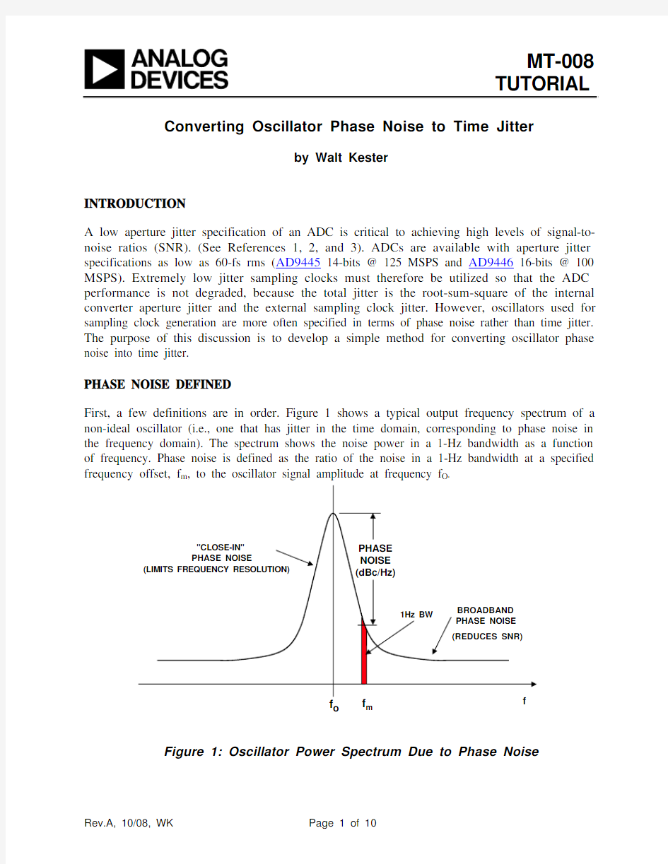
First, a few definitions are in order. Figure 1 shows a typical output frequency spectrum of a non-ideal oscillator (i.e., one that has jitter in the time domain, corresponding to phase noise in the frequency domain). The spectrum shows the noise power in a 1-Hz bandwidth as a function of frequency. Phase noise is defined as the ratio of the noise in a 1-Hz bandwidth at a specified frequency offset, f m, to the oscillator signal amplitude at frequency f O.
o m
Figure 1: Oscillator Power Spectrum Due to Phase Noise
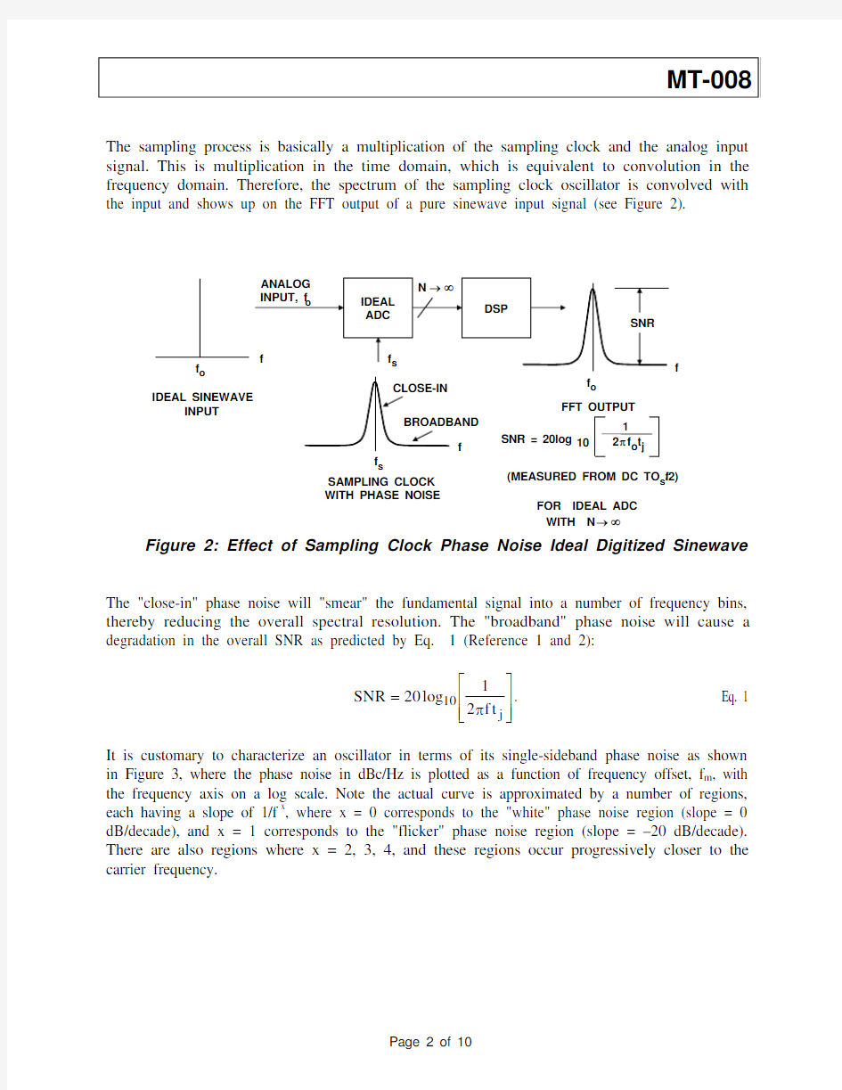
The sampling process is basically a multiplication of the sampling clock and the analog input signal. This is multiplication in the time domain, which is equivalent to convolution in the frequency domain. Therefore, the spectrum of the sampling clock oscillator is convolved with the input and shows up on the FFT output of a pure sinewave input signal (see Figure 2).
f o
f s
f o
IDEAL SINEWAVE
INPUT SAMPLING CLOCK WITH PHASE NOISE
FFT OUTPUT FOR IDEAL ADC WITH N →∞(MEASURED FROM DC TO f s /2)SNR = 20log 101
2πf o t j f f
Figure 2: Effect of Sampling Clock Phase Noise Ideal Digitized Sinewave
The "close-in" phase noise will "smear" the fundamental signal into a number of frequency bins, thereby reducing the overall spectral resolution. The "broadband" phase noise will cause a degradation in the overall SNR as predicted by Eq. 1 (Reference 1 and 2):
???
?
????π=j 10t f 21log 20SNR .
Eq. 1
It is customary to characterize an oscillator in terms of its single-sideband phase noise as shown in Figure 3, where the phase noise in dBc/Hz is plotted as a function of frequency offset, f m , with the frequency axis on a log scale. Note the actual curve is approximated by a number of regions, each having a slope of 1/f x , where x = 0 corresponds to the "white" phase noise region (slope = 0 dB/decade), and x = 1 corresponds to the "flicker" phase noise region (slope = –20 dB/decade). There are also regions where x = 2, 3, 4, and these regions occur progressively closer to the carrier frequency.
PHASE NOISE (dBc/Hz)
FREQUENCY OFFSET, f m , (LOG SCALE)
Figure 3: Oscillator Phase Noise in dBc/Hz vs. Frequency Offset
Note that the phase noise curve is somewhat analogous to the input voltage noise spectral density of an amplifier. Like amplifier voltage noise, low 1/f corner frequencies are highly desirable in an oscillator.
We have seen that oscillators are typically specified in terms of phase noise, but in order to relate phase noise to ADC performance, the phase noise must be converted into jitter. In order to make the graph relevant to modern ADC applications, the oscillator frequency (sampling frequency) is chosen to be 100 MHz for discussion purposes, and a typical graph is shown in Figure 4. Notice that the phase noise curve is approximated by a number of individual line segments, and the end points of each segment are defined by data points.
FREQUENCY OFFSET (Hz)PHASE
NOISE
(dBc/Hz)f m
Figure 4: Calculating Jitter from Phase Noise
CONVERTING PHASE NOISE TO JITTER
The first step in calculating the equivalent rms jitter is to obtain the integrated phase noise power assuming there is no filtering between the oscillator and the ADC input. This approximates the bandwidth of the ADC sampling clock input.
Selecting the lower frequency for the integration also requires some judgment. In theory, it should be as low as possible to get the true rms jitter. In practice, however, the oscillator specifications generally will not be given for offset frequencies less than 10 Hz, or so—however, this will certainly give accurate enough results in the calculations. A lower frequency of integration of 100 Hz is reasonable in most cases, if that specification is available. Otherwise, use either the 1-kHz or 10-kHz data point.
One should also consider that the "close-in" phase noise affects the spectral resolution of the system, while the broadband noise affects the overall system SNR. Probably the wisest approach is to integrate each area separately as explained below and examine the magnitude of the jitter contribution of each area. The low frequency contributions may be negligible compared to the broadband contribution if a crystal oscillator is used. Other types of oscillators may have significant jitter contributions in the low frequency area, and a decision must be made regarding their importance to the overall system frequency resolution.
The integration of each individual area yields individual power ratios. The individual power ratios are then summed and converted back into dBc. Once the integrated phase noise power is known, the rms phase jitter in radians is given by the equation (see References 3-7 for further details, derivations, etc.),
10/A 102)radians (Jitter Phase RMS ?=,
Eq. 2
and dividing by 2πf O converts the jitter in radians to jitter in seconds:
O
10
/A f 2102)onds (sec Jitter Phase RMS π?=
.
Eq. 3
It should be noted that computer programs and spreadsheets are available online to perform the integration by segments and calculate the rms jitter, thereby greatly simplifying the process (References 8, 9).
Figure 5 shows a sample calculation which assumes only broadband phase noise. The broadband phase noise chosen of –150 dBc/Hz represents a reasonably good signal generator specification, so the jitter number obtained represents a practical situation. The phase noise of –150 dBc/Hz (expressed as a ratio) is multiplied by the bandwidth of integration (200 MHz) to obtain the integrated phase noise of –67 dBc. Note that this multiplication is equivalent to adding the
quantity 10 log 10[200 MHz – 0.01 MHz] to the phase noise in dBc/Hz. In practice, the lower frequency limit of 0.01 MHz can be dropped from the calculation, as it does not affect the final result significantly. A total rms jitter of approximately 1 ps is obtained using Eq. 3.
10k
100k
1M
10M
100M
1G
FREQUENCY OFFSET (Hz)
PHASE NOISE (dBc/Hz)
f m
–150
RMS PHASE JITTER (radians) ≈2?10 = 6.32×10⁻⁴radians
A/10
RMS JITTER (seconds) =
RMS PHASE JITTER (radians)
2 πf O
A = –150dBc + 10 log 10
200×106–0.01×106
= –150dBc + 83dB = –67dBc
= 1ps
Figure 5: Sample Jitter Calculation Assuming Broadband Phase Noise
Crystal oscillators generally offer the lowest possible phase noise and jitter, and some examples are shown for comparison in Figure 6. All the oscillators shown have a typical 1/f corner frequency of 20 kHz, and the phase noise therefore represents the white phase noise level. The two Wenzel oscillators are fixed-frequency and represent excellent performance (Reference 9). It is difficult to achieve this level of performance with variable frequency signal generators, as shown by the –150 dBc specification for a relatively high quality generator.
Wenzel ULN Series*–174dBc/Hz @ 10kHz+
Wenzel Sprinter Series,–165dBc/Hz @ 10kHz+ High Quality Signal Generator –150dBc/Hz @ 10kHz+ z Thermal noise floor of resistive source in a matched system @ +25°C = –174dBm/Hz z 0dBm = 1mW = 632mV p-p into 50Ωz * An oscillator with an output of +13dBm (2.82V p-p) into 50Ωwith a phase noise of –174dBc/Hz has a noise floor of
+13dBm –174dBc = –161dBm, 13dB above the thermal noise floor (Wenzel ULN and Sprinter Series Specifications and Pricing Used with Permission of Wenzel Associates)
Figure 6: 100-MHz Oscillator Broadband Phase Noise Floor Comparisons (Wenzel ULN
and Sprinter Series Specifications and Pricing used with Permission of Wenzel
Associates)
At this point, it should be noted that there is a theoretical limit to the noise floor of an oscillator determined by the thermal noise of a matched source: –174 dBm/Hz at +25°C. Therefore, an oscillator with a +13-dBm output into 50 Ω (2.82-V p-p) with a phase noise of –174 dBc/Hz has a noise floor of –174 dBc + 13 dBm = –161 dBm. This is the case for the Wenzel ULN series as shown in Figure 6.
Figure 7 shows the jitter calculations from the two Wenzel crystal oscillators. In each case, the data points were taken directly for the manufacturer's data sheet. Because of the low 1/f corner frequency, the majority of the jitter is due to the "white" phase noise area. The calculated values of 64 fs (ULN-Series) and 180 fs represent extremely low jitter. For informational purposes, the individual jitter contributions of each area have been labeled separately. The total jitter is the root-sum-square of the individual jitter contributors.
1001k 10k 100k 1M 10M
PHASE
NOISE (dBc/Hz)
100
1k
10k
100k
1M
10M
PHASE
NOISE (dBc/Hz)
100M
100M
Figure 7: Jitter Calculations for Low Noise 100-MHz Crystal Oscillators
(Phase Noise Data used with Permission of Wenzel Associates)
In system designs requiring low jitter sampling clocks, the costs of low noise dedicated crystal oscillators is generally prohibitive. An alternative solution is to use a phase-locked-loop (PLL) in conjunction with a voltage-controlled oscillator to "clean up" a noisy system clock as shown in Figure 8. There are many good references on PLL design (see References 10-13, for example), and we will not pursue that topic further, other than to state that using a narrow bandwidth loop filter in conjunction with a voltage-controlled crystal oscillator (VCXO) typically gives the lowest phase noise. As shown in Figure 8, the PLL tends to reduce the "close-in" phase noise while at the same time, reducing the overall phase noise floor. Further reduction in the white noise floor can be obtained by following the PLL output with an appropriate bandpass filter.
f s
Figure 8: Using a Phase-Locked Loop (PLL) and Bandpass
Filter to Condition a Noisy Clock Source
The effect of enclosing a free-running VCO within a PLL is shown in Figure 9. Notice that the "close-in" phase noise is reduced significantly by the action of the PLL.
Figure 9: Phase Noise for a Free-Running VCO and a PLL-Connected VCO
Analog Devices offers a wide portfolio of frequency synthesis products, including DDS systems, N, and fractional-N PLLs. For example, the ADF4360 family are fully integrated PLLs complete with an internal VCO. With a 10-kHz bandwidth loop filter, the phase noise of the ADF4360-1 2.25-GHz PLL is shown in Figure 10, and the line-segment approximation and jitter calculations shown in Figure 11. Note that the rms jitter is only 1.57 ps, even with a non-crystal VCO.
PHASE NOISE (dBc/Hz)
Figure 10: Phase Noise for ADF4360-1 2.25-GHz PLL
with Loop Filter BW = 10 kHz
100
1k
10k
100k
1M 10M 100M 1G
4.5G
PHASE NOISE (dBc/Hz)
FREQUENCY OFFSET (Hz)
Figure 11: Line Segment Approximation to ADF4360-1, 2.25-GHz
PLL Phase Noise Showing Jitter
Historically, PLL design relied heavily on textbooks and application notes to assist in the design of the loop filter, etc. Now, with Analog Devices free downloadable ADIsimPLL? software, PLL design is much easier. To start, choose a circuit by entering the desired output frequency range, and select a PLL, VCO, and a crystal reference. Once the loop filter configuration has been selected, the circuit can be analyzed and optimized for phase noise, phase margin, gain, spur levels, lock time, etc., in both the frequency and time domain. The program also performs the rms jitter calculation based on the PLL phase noise, thereby allowing the evaluation of the final PLL output as a sampling clock.
SUMMARY
Sampling clock jitter can be disastrous to the SNR performance of high performance ADCs. Although the relationship between SNR and jitter is well known, most oscillators are specified in terms of their phase noise. This article has shown how to convert phase noise into jitter so that the SNR degradation can be easily calculated.
Although not as good as relatively expensive stand alone crystal oscillators, modern PLLs using crystal VCOs (along with suitable filtering) can achieve jitter performance suitable for all but the most demanding requirements.
The entire problem of clock distribution has become much more critical because of low jitter requirements. Analog Devices is now offering a line of clock distribution ICs to serve these needs (https://www.360docs.net/doc/e35413113.html,/clocks).
REFERENCES
1.Brad Brannon, "Aperture Uncertainty and ADC System Performance," Application Note AN-501, Analog
Devices, download at https://www.360docs.net/doc/e35413113.html,.
2.Bar-Giora Goldberg, "The Effects of Clock Jitter on Data Conversion Devices," RF Design, August 2002,
pp. 26-32, https://www.360docs.net/doc/e35413113.html,.
3.Ulrich L. Rohde, Digital PLL Frequency Synthesizers, Theory and Design, Prentice-Hall, 1983, ISBN 0-
13-214239-2, all of Chapter 2 and pp. 411-418 for computer analysis.
4.Joseph V. Adler, "Clock-Source Jitter: A Clear Understanding Aids Oscillator Selection," EDN, February
18, 1999, pp. 79-86, https://www.360docs.net/doc/e35413113.html,.
5.Neil Roberts, "Phase Noise and Jitter – A Primer for Digital Designers," EEdesign, July 14, 2003,
https://www.360docs.net/doc/e35413113.html,.
6.Boris Drakhlis, "Calculate Oscillator Jitter by using Phase-Noise Analysis Part 1," Microwaves and RF,
January 2001, p. 82, https://www.360docs.net/doc/e35413113.html,.
7.Boris Drakhlis, "Calculate Oscillator Jitter by using Phase-Noise Analysis Part 2," Microwaves and RF,
February 2001, p. 109, https://www.360docs.net/doc/e35413113.html,.
8.Raltron Electronics Corporation, 10651 Northwest 19th Street, Miami, Florida 33172, Tel: (305) 593-
6033, https://www.360docs.net/doc/e35413113.html,. (see "Convert SSB Phase Noise to Jitter" under "Engineering Design Tools").
9.Wenzel Associates, Inc., 2215 Kramer Lane, Austin, Texas 78758, Tel: (512) 835-2038,
https://www.360docs.net/doc/e35413113.html, (see "Allan Variance from Phase Noise" under "Spreadsheets").
10.Mike Curtin and Paul O'Brien, "Phase-Locked Loops for High-Frequency Receivers and Transmitters, Part
1, Analog Dialogue 33-3, 1999, https://www.360docs.net/doc/e35413113.html,.
11.Mike Curtin and Paul O'Brien, "Phase-Locked Loops for High-Frequency Receivers and Transmitters, Part
2, Analog Dialogue 33-5, 1999, https://www.360docs.net/doc/e35413113.html,.
12.R. E. Best, Phase-Locked Loops: Theory, Design and Applications, Fourth Edition, McGraw-Hill, 1999,
ISBN 0071349030.
13. F. M. Gardner, Phaselock Techniques, Second Edition, John Wiley, 1979, ISBN 0471042943.
Copyright 2009, Analog Devices, Inc. All rights reserved. Analog Devices assumes no responsibility for customer product design or the use or application of customers’ products or for any infringements of patents or rights of others which may result from Analog Devices assistance. All trademarks and logos are property of their respective holders. Information furnished by Analog Devices applications and development tools engineers is believed to be accurate and reliable, however no responsibility is assumed by Analog Devices regarding technical accuracy and topicality of the content provided in Analog Devices Tutorials.
古代晋灵公不君、齐晋鞌之战原文及译文
晋灵公不君(宣公二年) 原文: 晋灵公不君。厚敛以雕墙。从台上弹人,而观其辟丸也。宰夫胹熊蹯不熟,杀之,寘诸畚,使妇人载以过朝。赵盾、士季见其手,问其故而患之。将谏,士季曰:“谏而不入,则莫之继也。会请先,不入,则子继之。”三进及溜,而后视之,曰:“吾知所过矣,将改之。”稽首而对曰:“人谁无过?过而能改,善莫大焉。诗曰:‘靡不有初,鲜克有终。’夫如是,则能补过者鲜矣。君能有终,则社稷之固也,岂惟群臣赖之。又曰:‘衮职有阙,惟仲山甫补之。’能补过也。君能补过,衮不废矣。” 犹不改。宣子骤谏,公患之,使鉏麑贼之。晨往,寝门辟矣,盛服将朝。尚早,坐而假寐。麑退,叹而言曰:“不忘恭敬,民之主也。贼民之主,不忠;弃君之命,不信。有一于此,不如死也!”触槐而死。 秋九月,晋侯饮赵盾酒,伏甲将攻之。其右提弥明知之,趋登曰:“臣侍君宴,过三爵,非礼也。”遂扶以下。公嗾夫獒焉。明搏而杀之。盾曰:“弃人用犬,虽猛何为!”斗且出。提弥明死之。 初,宣子田于首山,舍于翳桑。见灵辄饿,问其病。曰:“不食三日矣!”食之,舍其半。问之,曰:“宦三年矣,未知母之存否。今近焉,请以遗之。”使尽之,而为之箪食与肉,寘诸橐以与之。既而与为公介,倒戟以御公徒,而免之。问何故,对曰:“翳桑之饿人也。”问其名居,不告而退。——遂自亡也。 乙丑,赵穿①攻灵公于桃园。宣子未出山而复。大史书曰:“赵盾弑其君。”以示于朝。宣子曰:“不然。”对曰:“子为正卿,亡不越竟,反不讨贼,非子而谁?”宣子曰:“呜呼!‘我之怀矣,自诒伊戚。’其我之谓矣。” 孔子曰:“董狐,古之良史也,书法不隐。赵宣子,古之良大夫也,为法受恶。惜也,越竞乃免。” 译文: 晋灵公不行君王之道。他向人民收取沉重的税赋以雕饰宫墙。他从高台上用弹弓弹人,然后观赏他们躲避弹丸的样子。他的厨子做熊掌,没有炖熟,晋灵公就把他杀了,把他的尸体装在草筐中,让宫女用车载着经过朝廷。赵盾和士季看到露出来的手臂,询问原由后感到很忧虑。他们准备向晋灵公进谏,士季说:“如果您去进谏而君王不听,那就没有人能够再接着进谏了。还请让我先来吧,不行的话,您再接着来。”士季往前走了三回,行了三回礼,一直到屋檐下,晋灵公才抬头看他。晋灵公说:“我知道我的过错了,我会改过的。”士季叩头回答道:“谁能没有过错呢?有过错而能改掉,这就是最大的善事了。《诗经》说:‘没有人向善没有一个开始的,但却很少有坚持到底的。’如果是这样,那么能弥补过失的人是很少的。您如能坚持向善,那么江山就稳固了,不只是大臣们有所依靠啊。
如何翻译古文
如何翻译古文 学习古代汉语,需要经常把古文译成现代汉语。因为古文今译的过程是加深理解和全面运用古汉语知识解决实际问题的过程,也是综合考察古代汉语水平的过程。学习古代汉语,应该重视古文翻译的训练。 古文翻译的要求一般归纳为信、达、雅三项。“信”是指译文要准确地反映原作的含义,避免曲解原文内容。“达”是指译文应该通顺、晓畅,符合现代汉语语法规范。“信”和“达”是紧密相关的。脱离了“信”而求“达”,不能称为翻译;只求“信”而不顾“达”,也不是好的译文。因此“信”和“达”是文言文翻译的基本要求。“雅”是指译文不仅准确、通顺,而且生动、优美,能再现原作的风格神韵。这是很高的要求,在目前学习阶段,我们只要能做到“信”和“达”就可以了。 做好古文翻译,重要的问题是准确地理解古文,这是翻译的基础。但翻译方法也很重要。这里主要谈谈翻译方法方面的问题。 一、直译和意译 直译和意译是古文今译的两大类型,也是两种不同的今译方法。 1.关于直译。所谓直译,是指紧扣原文,按原文的字词和句子进行对等翻译的今译方法。它要求忠实于原文,一丝不苟,确切表达原意,保持原文的本来面貌。例如: 原文:樊迟请学稼,子曰:“吾不如老农。”请学为圃。子曰:“吾不如老圃。”(《论语?子路》) 译文:樊迟请求学种庄稼。孔子道:“我不如老农民。”又请求学种菜蔬。孔子道:“我不如老菜农。”(杨伯峻《论语译注》) 原文:齐宣王问曰:“汤放桀,武王伐纣,有诸?”(《孟子?梁惠王下》) 译文:齐宣王问道:“商汤流放夏桀,武王讨伐殷纣,真有这回事吗?(杨伯峻《孟子译注》) 上面两段译文紧扣原文,字词落实,句法结构基本上与原文对等,属于直译。 但对直译又不能作简单化理解。由于古今汉语在文字、词汇、语法等方面的差异,今译时对原文作一些适当的调整,是必要的,并不破坏直译。例如: 原文:逐之,三周华不注。(《齐晋鞌之战》) 译文:〔晋军〕追赶齐军,围着华不注山绕了三圈。
环型振荡器(ring oscillator)的抖动(jitter)分析
Jitter and Phase Noise in Ring Oscillators Ali Hajimiri,Sotirios Limotyrakis,and Thomas H.Lee,Member,IEEE Abstract—A companion analysis of clock jitter and phase noise of single-ended and differential ring oscillators is presented.The impulse sensitivity functions are used to derive expressions for the jitter and phase noise of ring oscillators.The effect of the number of stages,power dissipation,frequency of oscillation,and short-channel effects on the jitter and phase noise of ring oscillators is analyzed.Jitter and phase noise due to substrate and supply noise is discussed,and the effect of symmetry on the upconversion of 1/f noise is demonstrated.Several new design insights are given for low jitter/phase-noise design.Good agreement between theory and measurements is observed. Index Terms—Design methodology,jitter,noise measurement, oscillator noise,oscillator stability,phase jitter,phase-locked loops,phase noise,ring oscillators,voltage-controlled oscillators. I.I NTRODUCTION D U E to their integrated nature,ring oscillators have be- come an essential building block in many digital and communication systems.They are used as voltage-controlled oscillators(VCO’s)in applications such as clock recovery circuits for serial data communications[1]–[4],disk-drive read channels[5],[6],on-chip clock distribution[7]–[10],and integrated frequency synthesizers[10],[11].Although they have not found many applications in radio frequency(RF), they can be used for some low-tier RF systems. Recently,there has been some work on modeling jitter and phase noise in ring oscillators.References[12]and[13] develop models for the clock jitter based on time-domain treatments for MOS and bipolar differential ring oscillators, respectively.Reference[14]proposes a frequency-domain approach to?nd the phase noise based on an linear time-invariant model for differential ring oscillators with a small number of stages. In this paper,we develop a parallel treatment of frequency-domain phase noise[15]and time-domain clock jitter for ring oscillators.We apply the phase-noise model presented in[16] to obtain general expressions for jitter and phase noise of the ring oscillators. The next section brie?y reviews the phase-noise model presented in[16].In Section III,we apply the model to timing jitter and develop an expression for the timing jitter of oscilla-tors,while Section IV provides the derivation of a closed-form expression to calculate the rms value of the impulse sensitivity function(ISF).Section V introduces expressions for jitter and phase noise in single-ended and differential ring oscillators Manuscript received April8,1998;revised November2,1998. A.Hajimiri is with the California Institute of Technology,Pasadena,CA 91125USA. S.Limotyrakis and T.H.Lee are with the Center for Integrated Systems, Stanford University,Stanford,CA94305USA. Publisher Item Identi?er S0018-9200(99)04200-6.in long-and short-channel regimes of operation.Section VI describes the effect of substrate and supply noise as well as the noise due to the tail-current source in differential struc-tures.Section VII explains the design insights obtained from this treatment for low jitter/phase-noise design.Section VIII summarizes the measurement results. II.P HASE N OISE The output of a practical oscillator can be written as is periodic in 2 model?uctuations in amplitude and phase due to internal and external noise sources.The amplitude?uctuations are signi?cantly attenuated by the amplitude limiting mechanism, which is present in any practical stable oscillator and is particularly strong in ring oscillators.Therefore,we will focus on phase variations,which are not quenched by such a restoring mechanism. As an example,consider the single-ended ring oscillator with a single current source on one of the nodes shown in Fig.1.Suppose that the current source consists of an impulse of current with area is proportional to the injected charge (3) where is the voltage swing across the capacitor and thus represents the sensitivity of every point of the waveform to a perturbation,
齐晋鞌之战原文和译文
鞌之战选自《左传》又名《鞍之战》原文:楚癸酉,师陈于鞌(1)。邴夏御侯,逢丑父为右②。晋解张御克,郑丘缓为右(3)。侯日:“余姑翦灭此而朝食(4)”。不介马而驰之⑤。克伤于矢,流血及屦2 未尽∧6),曰:“余病矣(7)!”张侯曰:“自始合(8),而矢贯余手及肘(9),余折以御,左轮朱殷(10),岂敢言病吾子忍之!”缓曰:“自始合,苟有险,余必下推车,子岂_识之(11)然子病矣!”张侯曰:“师之耳目,在吾旗鼓,进退从之。此车一人殿之(12),可以集事(13),若之何其以病败君之大事也擐甲执兵(14),固即死也(15);病未及死,吾子勉之(16)!”左并辔(17) ,右援拐鼓(18)。马逸不能止(19),师从之,师败绩。逐之,三周华不注(20) 韩厥梦子舆谓己曰:“旦辟左右!”故中御而从齐侯。邴夏曰:“射其御者,君子也。”公曰:“谓之君子而射之,非礼也。”射其左,越于车下;射其右,毙于车中。綦毋张丧车,从韩厥,曰:“请寓乘。”从左右,皆肘之,使立于后。韩厥俛,定其右。逢丑父与公易位。将及华泉,骖絓于木而止。丑父寝于轏中,蛇出于其下,以肱击之,伤而匿之,故不能推车而及。韩厥执絷马前,再拜稽首,奉觞加璧以进,曰:“寡君使群臣为鲁、卫请,曰:‘无令舆师陷入君地。’下臣不幸,属当戎行,无所逃隐。且惧奔辟而忝两君,臣辱戎士,敢告不敏,摄官承乏。” 丑父使公下,如华泉取饮。郑周父御佐车,宛茷为右,载齐侯以免。韩厥献丑父,郤献子将戮之。呼曰:“自今无有代其君任患者,有一于此,将为戮乎”郤子曰:“人不难以死免其君,我戮之不祥。赦之,以劝事君者。”乃免之。译文1:在癸酉这天,双方的军队在鞌这个地方摆开了阵势。齐国一方是邴夏为齐侯赶车,逢丑父当车右。晋军一方是解张为主帅郤克赶车,郑丘缓当车右。齐侯说:“我姑且消灭了这些人再吃早饭。”不给马披甲就冲向了晋军。郤克被箭射伤,血流到了鞋上,但是仍不停止擂鼓继续指挥战斗。他说:“我受重伤了。”解张说:“从一开始接战,一只箭就射穿了我的手和肘,左边的车轮都被我的血染成了黑红色,我哪敢说受伤您忍着点吧!”郑丘缓说:“从一开始接战,如果遇到道路不平的地方,我必定(冒着生命危险)下去推车,您难道了解这些吗不过,您真是受重伤了。”daier 解张说:“军队的耳朵和眼睛,都集中在我们的战旗和鼓声,前进后退都要听从它。这辆车上还有一个人镇守住它,战事就可以成功。为什么为了伤痛而败坏国君的大事呢身披盔甲,手执武器,本来就是去走向死亡,伤痛还没到死的地步,您还是尽力而为吧。”一边说,一边用左手把右手的缰绳攥在一起,用空出的右手抓过郤克手中的鼓棰就擂起鼓来。(由于一手控马,)马飞快奔跑而不能停止,晋军队伍跟着指挥车冲上去,把齐军打得打败。晋军随即追赶齐军,三次围绕着华不注山奔跑。韩厥梦见他去世的父亲对他说:“明天早晨作战时要避开战车左边和右边的位置。”因此韩厥就站在中间担任赶车的来追赶齐侯的战车。邴夏说:“射那个赶车的,他是个君子。”齐侯说: “称他为君子却又去射他,这不合于礼。”daier 于是射车左,车左中箭掉下了车。又射右边的,车右也中箭倒在了车里。(晋军的)将军綦毋张损坏了自己的战车,跟在韩厥的车后说: “请允许我搭乗你的战车。”他上车后,无论是站在车的左边,还是站在车的右边,韩厥都用肘推他,让他站在自己身后——战车的中间。韩厥又低下头安定了一下受伤倒在车中的那位自己的车右。于是逢丑父和齐侯(乘韩厥低头之机)互相调换了位置。将要到达华泉时,齐侯战车的骖马被树木绊住而不能继续逃跑而停了下来。(头天晚上)逢丑父睡在栈车里,有一条蛇从他身子底下爬出来,他用小臂去打蛇,小臂受伤,但他(为了能当车右)隐瞒了这件事。由于这样,他不能用臂推车前进,因而被韩厥追上了。韩厥拿着拴马绳走到齐侯的马前,两次下拜并行稽首礼,捧着一杯酒并加上一块玉璧给齐侯送上去,
技术指标学习——Stochastic Oscillator (随机摆动指标)(翻译 整理)
技术指标学习——Stochastic Oscillator (随机摆动指标)(翻译 +整理) Stochastics指标用于帮助我们判断一个趋势是否结束。它定义为:一个Stochastic指标是一个振动器用于衡量市场中的超买、超卖的情况。其中的两条线类似于MACD中的线条,一条比另一条快速。 如何使用Stochastics指标 像我们早先所说的,Stochastics指标告诉我们何时市场出现超买或者超卖。Stochastics指标的值按比例从0到100。当Stochastics线条超越70(上图中红色点线处),则说明市场处于超买状态。当Stochastics线条低于30(蓝色点线处),说明市场处于超卖状态。作为一个经验法则,我们在市场处于超卖时买入,在市场处于超买时卖出。 看看上图,你会发现Stochastics指标在相当长的一段时间内显示出超买状况。基于以上的这些信息,你能猜到价格的走势吗? 如果你说价格将下跌,那你就对了!因为市场长时间处于超
买状态,扭转是必然会发生的。 这是最基本的Stochastics指标。许多交易者以不同的方式利用Stochastics指标,但这个指标的主要目的是为了告诉我们当前的市场何时是超买超卖。随着时间的推移,你将学会把Stochastics指标融入你自己的个人交易风格中。 原文(https://www.360docs.net/doc/e35413113.html,/school/stochastics.html)Stochastics指标又名KDJ 指标,是由George Lane 首创的,最早用于期货市场。Stochastics指标在图表上采用%K和%D 两条线,在设计中综合了动量观念、强弱指标与移动平均线的优点,在计算过程中主要研究高低价位与收市价的关系,反映价格走势的强弱和超买超卖现象。它的主要理论依据是:当价格上涨时,收市价倾向于接近当日价格区间的上端;相反,在下降趋势中收市价趋向于接近当日价格区间的下端。在股市和期市中,因为市场趋势上升而未转向前,每日多数都会偏向于高价位收市,而下跌时收市价就常会偏于低位。随机指数在设计中充分考虑价格波动的随机振幅与中短期波动的测算,使其短期测市功能比移动平均线更加准确有效,在市场短期超买超卖的预测方面又比强弱指数敏感,因此,这一指标被投资者广泛采用。 Stochastics指标对比给定的一段时期里,价格的范围同价格收市价(close)的相关情况。该振荡指标以双线来显示。主线被称为%K线。第二根线被称为%D线,它的数值是主线%K
《鞌之战》阅读答案(附翻译)原文及翻译
《鞌之战》阅读答案(附翻译)原文及翻 译 鞌之战[1] 选自《左传成公二年(即公元前589年)》 【原文】 癸酉,师陈于鞌[2]。邴夏御齐侯[3],逢丑父为右[4]。晋解张御郤克,郑丘缓为右[5]。齐侯曰:余姑翦灭此而朝食[6]。不介马而驰之[7]。郤克伤于矢,流血及屦,未绝鼓音[8],曰:余病[9]矣!张侯[10]曰:自始合,而矢贯余手及肘[11],余折以御,左轮朱殷[12],岂敢言病。吾子[13]忍之!缓曰:自始合,苟有险[14],余必下推车,子岂识之[15]?然子病矣!张侯曰:师之耳目,在吾旗鼓,进退从之[16]。此车一人殿之[17],可以集事[18],若之何其以病败君之大事也[19]?擐甲执兵,固即死也[20]。病未及死,吾子勉之[21]!左并辔[22],右援枹而鼓[23],马逸不能止[24],师从之。齐师败绩[25]。逐之,三周华不注[26]。 【注释】 [1]鞌之战:春秋时期的著名战役之一。战争的实质是齐、晋争霸。由于齐侯骄傲轻敌,而晋军同仇敌忾、士气旺盛,战役以齐败晋胜而告终。鞌:通鞍,齐国地名,在今山东济南西北。 [2]癸酉:成公二年的六月十七日。师,指齐晋两国军队。陈,
列阵,摆开阵势。 [3]邴夏:齐国大夫。御,动词,驾车。御齐侯,给齐侯驾车。齐侯,齐国国君,指齐顷公。 [4]逢丑父:齐国大夫。右:车右。 [5]解张、郑丘缓:都是晋臣,郑丘是复姓。郤(x )克,晋国大夫,是这次战争中晋军的主帅。又称郤献子、郤子等。 [6]姑:副词,姑且。翦灭:消灭,灭掉。朝食:早饭。这里是吃早饭的意思。这句话是成语灭此朝食的出处。 [7]不介马:不给马披甲。介:甲。这里用作动词,披甲。驰之:驱马追击敌人。之:代词,指晋军。 [8] 未绝鼓音:鼓声不断。古代车战,主帅居中,亲掌旗鼓,指挥军队。兵以鼓进,击鼓是进军的号令。 [9] 病:负伤。 [10]张侯,即解张。张是字,侯是名,人名、字连用,先字后名。 [11]合:交战。贯:穿。肘:胳膊。 [12]朱:大红色。殷:深红色、黑红色。 [13]吾子:您,尊敬。比说子更亲切。 [14]苟:连词,表示假设。险:险阻,指难走的路。 [15]识:知道。之,代词,代苟有险,余必下推车这件事,可不译。 [16]师之耳目:军队的耳、目(指注意力)。在吾旗鼓:在我们
《鞌之战》阅读答案附翻译
《鞌之战》阅读答案(附翻译) 《鞌之战》阅读答案(附翻译) 鞌之战[1] 选自《左传·成公二年(即公元前589年)》 【原文】 癸酉,师陈于鞌[2]。邴夏御齐侯[3],逢丑父为右[4]。晋解张御郤克,郑丘缓为右[5]。齐侯曰:“余姑 翦灭此而朝食[6]。”不介马而驰之[7]。郤克伤于矢, 流血及屦,未绝鼓音[8],曰:“余病[9]矣!”张侯[10]曰:“自始合,而矢贯余手及肘[11],余折以御,左轮 朱殷[12],岂敢言病。吾子[13]忍之!”缓曰:“自始合,苟有险[14],余必下推车,子岂识之[15]?——然 子病矣!”张侯曰:“师之耳目,在吾旗鼓,进退从之[16]。此车一人殿之[17],可以集事[18],若之何其以 病败君之大事也[19]?擐甲执兵,固即死也[20]。病未 及死,吾子勉之[21]!”左并辔[22],右援枹而鼓[23],马逸不能止[24],师从之。齐师败绩[25]。逐之,三周 华不注[26]。 【注释】 [1]鞌之战:春秋时期的著名战役之一。战争的实质是齐、晋争霸。由于齐侯骄傲轻敌,而晋军同仇敌忾、 士气旺盛,战役以齐败晋胜而告终。鞌:通“鞍”,齐
国地名,在今山东济南西北。 [2]癸酉:成公二年的六月十七日。师,指齐晋两国军队。陈,列阵,摆开阵势。 [3]邴夏:齐国大夫。御,动词,驾车。御齐侯,给齐侯驾车。齐侯,齐国国君,指齐顷公。 [4]逢丑父:齐国大夫。右:车右。 [5]解张、郑丘缓:都是晋臣,“郑丘”是复姓。郤(xì)克,晋国大夫,是这次战争中晋军的主帅。又称郤献子、郤子等。 [6]姑:副词,姑且。翦灭:消灭,灭掉。朝食:早饭。这里是“吃早饭”的意思。这句话是成语“灭此朝食”的出处。 [7]不介马:不给马披甲。介:甲。这里用作动词,披甲。驰之:驱马追击敌人。之:代词,指晋军。 [8]未绝鼓音:鼓声不断。古代车战,主帅居中,亲掌旗鼓,指挥军队。“兵以鼓进”,击鼓是进军的号令。 [9]病:负伤。 [10]张侯,即解张。“张”是字,“侯”是名,人名、字连用,先字后名。 [11]合:交战。贯:穿。肘:胳膊。 [12]朱:大红色。殷:深红色、黑红色。 [13]吾子:您,尊敬。比说“子”更亲切。
振荡器(Crystal Oscillator)与谐振器(Resonator)的比较
振荡器(Crystal Oscillator)与谐振器(Resonator) 两者区别: 振荡器是有源元件,将直流信号转换为交流信号,其等效电路是一个电容与一个电阻并联,再与一个电容串联,该电路有两个谐振点。 谐振器是无源元件,需要外围电路,驱动,其原理是压电效应。 相比较之下,振荡器输出信号质量好,但是信号电平单一,且价格高,用于高精度要求的场合。 元件化的振荡器有晶体振荡器和硅振荡器等;谐振器有晶体谐振器与陶瓷谐振器。 以下为摘录。 晶体谐振器 石英晶体俗称水晶,成分SIO2,是重要的压电材料,其主要特征是其原子或分子有规律排列,反映在宏观上是外形的对称性。在电场的作用下,晶体内部产生应力而形变,从而产生机械振动,获得特定的频率,利用它的这种逆压电效应特性来制造石英晶体谐振器。石英由于具备天然的高品质因子“Q”,这使得晶体能在整个工作温度和电压范围内都保持很高的精确度和频率稳定性。 优点:信号电平是可变的,也就是说是根据起振电路来决定的,同样的晶体可以适用于多种电压,可用于多种不同时钟信号电压要求的片子,而且价格通常也较低。晶体谐振器的精度为1PPM(百万分之一)至100PPM。 缺点:晶体谐振器是有2个引脚的无极性元件,需要借助于时钟电路才能产生振荡信号,自身无法振荡起来。晶体谐振器相对于晶体振荡器而言其缺陷是信号质量较差,通常需要精确匹配外围电路(用于信号匹配的电容、电感、电阻等),更换不同频率的晶体时周边配置电路需要做相应的调整。 晶体谐振器有一些等效参数,不同的使用环境可能会有不同的要求,选用时还要考虑环境温度、负载电容、频率精度等要求,这就要求外围振荡电路的参数要加一些控制才能输出稳定的频率。 陶瓷谐振器 陶瓷谐振器是一种用于在特定频率产生振荡的压电式陶瓷设备。制造这种设备所用的材料在生产过程期间会激发谐振特性。由于这种谐振特性是处于生产误差范围内的,并且它的品质因数远远低于石英的品质因数,因此陶瓷谐振器所能提供的频率稳定性不如晶体谐振器。通常陶瓷谐振器用于对成本较低且对性能要求不高的场合。 优点:同晶体相比,陶瓷谐振器的成本只有晶体的一半并且尺寸较小。 缺点:同晶体相比,欠缺频率和温度稳定性。其精度较差,大概在1%至0.1%之间。 综述:陶瓷谐振器的典型初始精度在0.5%至0.1%范围内,老化或温度变化所致的漂移可能改变这一精度范围。廉价陶瓷谐振器的公差只有±1.1%,较高端的汽车精度则分别为±0.25%和±0.3%。未来的应用在于汽车CAN(控制器局域网络)总线应用,工作温度为-40°C 至+125°C。频率为200 KHZ至约1 GHZ的低成本陶瓷谐振器适用于对时序要求不严格的嵌入系统。陶瓷器件起动较快,一般体积小于石英器件。它们也更能承受冲击与振动。 晶体振荡器 优点:晶体振荡器信号质量好,比较稳定,而且连接方式相对简单(主要是做好电源滤波,通常使用一个电容和电感构成的PI型滤波网络,输出端用一个小阻值的电阻过滤信号即可),不需要复杂的配置电路。对于时序要求敏感的应用,晶体振荡器的性能相对较好。 缺点:相对于晶体谐振器,晶体振荡器的缺陷是其信号电平是固定的,需要选择好合适
左传《齐晋鞌之战》原文+翻译+注释
左传《齐晋鞌之战》原文+翻译+注释 楚癸酉,师陈于鞌(1)。邴夏御侯,逢丑父为右②。晋解张御克,郑丘缓 为右(3)。侯日:“余姑翦灭此而朝食(4)”。不介马而驰之⑤。克伤于矢, 流血及屦2未尽∧?6),曰:“余病矣(7)!”张侯曰:“自始合(8),而矢贯余手 及肘(9),余折以御,左轮朱殷(10),岂敢言病?吾子忍之!”缓曰:“自始合,苟有险,余必下推车,子岂_识之(11)?然子病矣!”张侯曰:“师之耳目,在 吾旗鼓,进退从之。此车一人殿之(12),可以集事(13),若之何其以病败君之大事也?擐甲执兵(14),固即死也(15);病未及死,吾子勉之(16)!”左并辔(17) ,右援拐?鼓(18)。马逸不能止(19),师从之,师败绩。逐之,三周华不注(20) 韩厥梦子舆谓己曰:“旦辟左右!”故中御而从齐侯。邴夏曰:“射其御者,君子也。”公曰:“谓之君子而射之,非礼也。”射其左,越于车下;射其右,毙于车中。綦毋张丧车,从韩厥,曰:“请寓乘。”从左右,皆肘之,使立于后。韩厥俛,定其右。逢丑父与公易位。将及华泉,骖絓于木而止。丑父寝于轏中,蛇出于其下,以肱击之,伤而匿之,故不能推车而及。韩厥执絷马前,再拜稽首,奉觞加璧以进,曰:“寡君使群臣为鲁、卫请,曰:‘无令舆师陷入君地。’下臣不幸,属当戎行,无所逃隐。且惧奔辟而忝两君,臣辱戎士,敢告不敏,摄官承乏。”丑父使公下,如华泉取饮。郑周父御佐车,宛茷为右,载齐侯以免。韩厥献丑父,郤献子将戮之。呼曰:“自今无有代其君任患者,有一于此,将为戮乎?”郤子曰:“人不难以死免其君,我戮之不祥。赦之,以劝事君者。”乃免之。 在癸酉这天,双方的军队在鞌这个地方摆开了阵势。齐国一方是邴夏为齐侯赶车,逢丑父当车右。晋军一方是解张为主帅郤克赶车,郑丘缓当车右。齐侯说:“我姑且消灭了这些人再吃早饭。”不给马披甲就冲向了晋军。郤克被箭射伤,血流到了鞋上,但是仍不停止擂鼓继续指挥战斗。他说:“我受重伤了。”解张说:“从一开始接战,一只箭就射穿了我的手和肘,左边的车轮都被我的血染成了黑红色,我哪敢说受伤?您忍着点吧!”郑丘缓说:“从一开始接战,如果遇到道路不平的地方,我必定(冒着生命危险)下去推车,您难道了解这些吗?不过,您真是受重伤了。”daier解张说:“军队的耳朵和眼睛,都集中在我们的战旗和鼓声,前进后退都要听从它。这辆车上还有一个人镇守住它,战事就可以成功。为什么为了伤痛而败坏国君的大事呢?身披盔甲,手执武器,本来就是去走向死亡,伤痛还没到死的地步,您还是尽力而为吧。”一边说,一边用左手把右手的缰绳攥在一起,用空出的右手抓过郤克手中的鼓棰就擂起鼓来。(由于一手控马,)马飞快奔跑而不能停止,晋军队伍跟着指挥车冲上去,把齐军打得打败。晋军随即追赶齐军,三次围绕着华不注山奔跑。
7050SMD HCSL Crystal Oscillator
OT Type 7.0 x 5.0 mm SMD HCSL Crystal Oscillator Specifications subject to change without notice Rev(2)12/2012 FEATURE - Typical 7.0 x 5.0 x 1.5 mm hermetically sealed ceramic package. - Very low jitter performance :Max. 0.5 pS RMS from 12k-20MHz. - Tight symmetry (45 to 55%) available. - Tri-state enable/disable. - High-speed current steering logic (HCSL) output. TYPICAL APPLICATION - PCI-Express RoHS Compliant Standard ELECTRICAL SPECIFICATION HCSL 3.3V 2.5V Parameter Min. Max. Min. Max. Unit Supply Voltage Variation (V DD ) 5% 3.135 3.465 2.375 2.625 V Frequency Range 90 125 90 125 Standard Frequency 100 MHz Supply Current 90MHz ≦ F0 ≦ 125MHz - 30 - 30 mA Output Level Output High (Logic “1”) 0.6 - 0.58 - Output Low (Logic “0”) - 0.15 - 0.15 V Transition Time:Rise/Fall Time+ - 0.5 - 0.5 nSec Start Time - 3 - 3 mSec Tri-State(Input to Pin 2 or Pin 1) Enable 0.7V DD - 0.7V DD - Disable - 0.3V DD - 0.3V DD V RMS Phase Jitter (integrated 12KHz ~ 20MHz) 90MHz ≦ F0 ≦ 125MHz - 0.5 - 0.5 pSec Aging - ±3 - ±3 ppm Storage Temp. Range -55 125 -55 125 ℃ Standard frequencies are frequencies which the crystal has been designed and does not imply a stock position +Transition times are measured between 20% and 80% of V DD Packing: Tape & Reel, 1000/3000pcs per Reel * O: Standard △:Available (case by case) X: Not available *Inclusive of calibration @ 25℃, operating temperature range, input voltage variation, 深圳捷比信--高品质精密元件供应商 www.jepsun.com
AO动能技术指标震荡指标Awesome OScillator
震荡指标 AO动能技术指标是(AO)34段简单移动平均线,其轨迹通过柱形中间点(H-L)/2,这一点是从五段简单移动平均线中扣除的,它建立在横跨(H-L)/2柱形中间的那点上,并且向我们清楚的显示了当前市场趋势的一个状况。 购买的信号 茶托 T只有当柱形图高于零点线时,唯一的购买信号才会到来。我们必须牢记: ?当柱形图由下降的趋势变化为上升时,才产生“茶托”购买信号。第二栏比第一栏低,并且第二栏是红色。 ?第三栏比第二栏高,而且第三栏是绿色的。 请记住:为了能使用“茶托”信号,所有的AO动能指标都应超过零点线。 零点线相交 当柱形图由负值的区域向正值的区域过度时,会产生购买的信号。当柱形图通过零点线以后,购买信号也随之而来。关于这个信号: ?为了使信号产生,我们只需要两栏; ?第一栏应该低于零点线,第二栏应该穿过它。(从负值转化为正值); ?购买信号和卖出信号同时产生是不可能的。 两个箭头 当柱形图的价值低于零点线,唯一的购买信号才会产生。关于这个信号,我们请牢记: ?当你有一个向下的箭头(最小值),并且这一点低于零点线,还有一个方向同时往下的尖头紧随其后,它的位置比上一个箭头稍高一点。其绝对值比较小(因此离开零点更近一些),在这种情况下,购买信号才会产生?柱形图低于两个箭头之间的零点线。如果柱形图穿过两个箭头之间的部分,购买的信号不会起作用。当然,与零点线相交时,购买信号会产生。 ?柱形图的每一个新的箭头(一个接近零点线并且绝对值比较小的那个负数)其数值高于前一个箭头。
如果形成了另外一个数值较高的箭头(接近零点线),并且柱形图没有穿过零点,那么会产生一个额外的购买信号。 卖出信号 AO动量指标的卖出信号和购买信号相同。“茶拖”信号则相反,而且其低于零点线,穿过零点线的机会会减小——第一栏高于零点线,第二栏低于零点线。两个箭头的信号高于零点线也可低于零点线。 计算方法 AO34段简单移动平均线,其轨迹通过柱形中间点(H-L)/2,这一点是从五段简单移动平均线中扣除的,它建立在横跨(H+L)/2柱形中间的那点上。 MEDIAN PRICE = (HIGH+LOW)/2 AO = SMA(MEDIAN PRICE, 5)-SMA(MEDIAN PRICE, 34) 注解: SMA —简单移动平均值..
《鞌之战》阅读答案(附翻译)
鞌之战[1]选自《左传·成公二年(即公元前589年)》【原文】癸酉,师陈于鞌[2]。邴夏御齐侯[3],逢丑父为右[4]。晋解张御郤克,郑丘缓为右[5]。齐侯曰:“余姑翦灭此而朝食[6]。”不介马而驰之[7]。郤克伤于矢,流血及屦,未绝鼓音[8],曰:“余病[9]矣!”张侯[10]曰:“自始合,而矢贯余手及肘[11],余折以御,左轮朱殷[12],岂敢言病。吾子[13]忍之!”缓曰:“自始合,苟有险[14],余必下推车,子岂识之[15]?——然子病矣!”张侯曰:“师之耳目,在吾旗鼓,进退从之[16]。此车一人殿之[17],可以集事[18],若之何其以病败君之大事也[19]?擐甲执兵,固即死也[20]。病未及死,吾子勉之[21]!”左并辔[22],右援枹而鼓[23],马逸不能止[24],师从之。齐师败绩[25]。逐之,三周华不注[26]。【注释】 [1]鞌之战:春秋时期的著名战役之一。战争的实质是齐、晋争霸。由于齐侯骄傲轻敌,而晋军同仇敌忾、士气旺盛,战役以齐败晋胜而告终。鞌:通“鞍”,齐国地名,在今山东济南西北。 [2]癸酉:成公二年的六月十七日。师,指齐晋两国军队。陈,列阵,摆开阵势。 [3]邴夏:齐国大夫。御,动词,驾车。御齐侯,给齐侯驾车。齐侯,齐国国君,指齐顷公。 [4]逢丑父:齐国大夫。右:车右。 [5]解张、郑丘缓:都是晋臣,“郑丘”是复姓。郤(xì)克,晋国大夫,是这次战争中晋军的主帅。又称郤献子、郤子等。 [6]姑:副词,姑且。翦灭:消灭,灭掉。朝食:早饭。这里是“吃早饭”的意思。这句话是成语“灭此朝食”的出处。 [7]不介马:不给马披甲。介:甲。这里用作动词,披甲。驰之:驱马追击敌人。之:代词,指晋军。 [8] 未绝鼓音:鼓声不断。古代车战,主帅居中,亲掌旗鼓,指挥军队。“兵以鼓进”,击鼓是进军的号令。 [9] 病:负伤。 [10]张侯,即解张。“张”是字,“侯”是名,人名、字连用,先字后名。 [11]合:交战。贯:穿。肘:胳膊。 [12]朱:大红色。殷:深红色、黑红色。 [13]吾子:您,尊敬。比说“子”更亲切。 [14]苟:连词,表示假设。险:险阻,指难走的路。 [15]识:知道。之,代词,代“苟有险,余必下推车”这件事,可不译。 [16]师之耳目:军队的耳、目(指注意力)。在吾旗鼓:在我们的旗子和鼓声上。进退从之:前进、后退都听从它们。 [17]殿之:镇守它。殿:镇守。 [18]可以集事:可以(之)集事,可以靠它(主帅的车)成事。集事:成事,指战事成功。 [19]若之何:固定格式,一般相当于“对……怎么办”“怎么办”。这里是和语助词“其”配合,放在谓语动词前加强反问,相当于“怎么”“怎么能”。以,介词,因为。败,坏,毁坏。君,国君。大事,感情。古代国家大事有两件:祭祀与战争。这里指战争。 [20]擐:穿上。执兵,拿起武器。 [21]勉,努力。 [22]并,动词,合并。辔(pèi):马缰绳。古代一般是四匹马拉一车,共八条马缰绳,两边的两条系在车上,六条在御者手中,御者双手执之。“左并辔”是说解张把马缰绳全合并到左手里握着。 [23]援:拿过来。枹(fú):击鼓槌。鼓:动词,敲鼓。 [24]逸:奔跑,狂奔。 [25] 败绩:大败。 [26] 周:环绕。华不注:山名,在今山东济南东北。【译文】六月十七日,齐晋两军在鞌地摆开阵势。邴夏为齐侯驾车,逢丑父担任车右做齐侯的护卫。晋军解张替郤克驾车,郑丘缓做了郤克的护卫。齐侯说:“我姑且消灭了晋军再吃早饭!”齐军没有给马披甲就驱车进击晋军。郤克被箭射伤,血一直流到鞋上,但他一直没有停止击鼓进。并说:“我受重伤了!”解张说:“从开始交战,箭就射穿了我的手和胳膊肘,我折断箭杆继续驾车,左边的车轮被血染得深红色,哪里敢说受了重伤?您还是忍住吧。”郑丘缓说:“从开始交战,只要遇到险峻难走的路,我必定要下去推车,您哪里知道这种情况呢?——不过您确实受重伤了!”解张说:“我们的旗帜和战鼓是军队的耳目,或进或退都听从旗鼓指挥。这辆战车只要一人镇守,就可以凭它成事。怎么能因为受伤而败坏国君的大事呢?穿上铠甲,拿起武器,本来就抱定了必死的决心。您虽然受了重伤还没有到死的地步,您就尽最大的努力啊!”于是左手把马缰绳全部握在一起,右手取过鼓槌来击鼓。战马狂奔不止,晋军跟着主帅的车前进。齐军大败,晋军追击齐军,绕着华不注山追了三圈。
Oscillator Phase Noise A Tutorial
Oscillator Phase Noise:A Tutorial Thomas H.Lee,Member,IEEE,and Ali Hajimiri,Member,IEEE Abstract—Linear time-invariant(LTI)phase noise theories provide important qualitative design insights but are limited in their quantitative predictive power.Part of the difficulty is that device noise undergoes multiple frequency translations to become oscillator phase noise.A quantitative understanding of this process requires abandoning the principle of time invariance assumed in most older theories of phase noise.Fortunately,the noise-to-phase transfer function of oscillators is still linear,despite the existence of the nonlinearities necessary for amplitude stabilization.In addi- tion to providing a quantitative reconciliation between theory and measurement,the time-varying phase-noise model presented in this tutorial identifies the importance of symmetry in suppressing the upconversion of1