LTC6910-1CTS8中文资料
1
2
6910123fa
Total Supply Voltage (V+ to V–)............................. 11V Input Current ..................................................... ±25mA Operating Temperature Range (Note 2)
LTC6910-1C, -2C, -3C........................–40°C to 85°C LTC6910-1I, -2I, -3I ...........................–40°C to 85°C LTC6910-1H, -2H, -3H .................... –40°C to 125°C Specified Temperature Range (Note 3)
LTC6910-1C, -2C, -3C........................–40°C to 85°C LTC6910-1I, -2I, -3I ...........................–40°C to 85°C LTC6910-1H, -2H, -3H .................... –40°C to 125°C Storage Temperature Range.................–65°C to 150°C Lead Temperature (Soldering, 10 sec)..................300°C
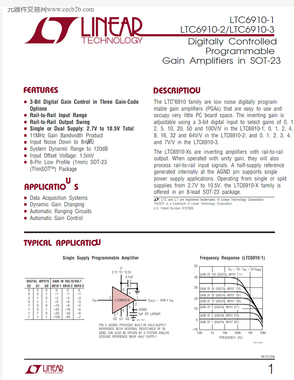
ORDER PART NUMBER
T JMAX = 150°C, θJA = 230°C/W
LTC6910-1CTS8LTC6910-1ITS8LTC6910-1HTS8LTC6910-2CTS8LTC6910-2ITS8LTC6910-2HTS8LTC6910-3CTS8LTC6910-3ITS8LTC6910-3HTS8(Note 1)
TS8 PART MARKING*LTB5 (6910-1)LTACQ (6910-2)LTACS (6910-3)
ABSOLUTE AXI U RATI GS
W
W W
U PACKAGE/ORDER I FOR ATIO
U U W
Consult LTC Marketing for parts specified with wider operating temperature ranges.*The temperature grades are identified by a label on the shipping container.
OUT 1AGND 2IN 3V – 4
8 V +7 G26 G15 G0
TOP VIEW
TS8 PACKAGE
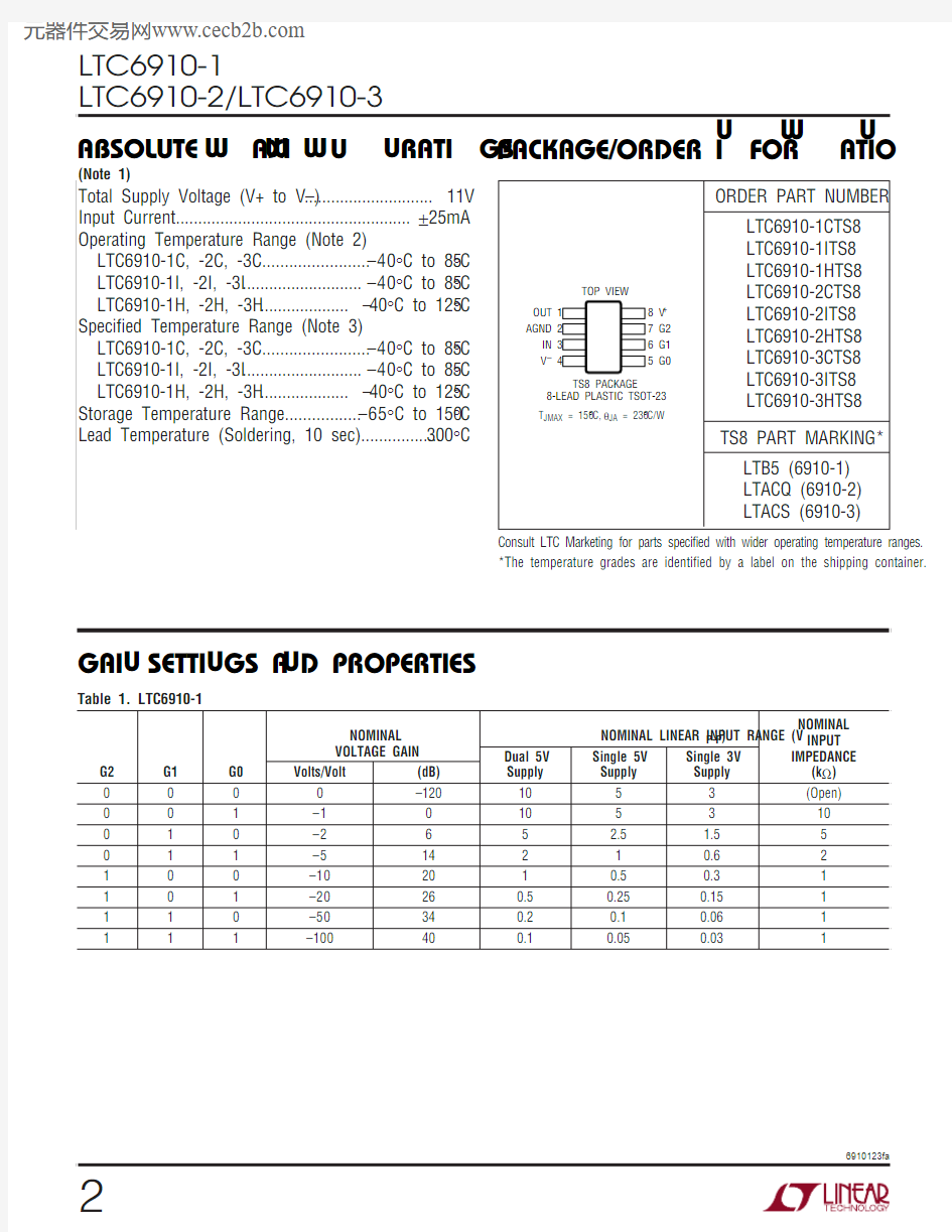
8-LEAD PLASTIC TSOT-23Table 1. LTC6910-1
NOMINAL
NOMINAL NOMINAL LINEAR INPUT RANGE (V P-P )INPUT VOLTAGE GAIN Dual 5V Single 5V Single 3V IMPEDANCE G2G1G0Volts/Volt (dB)Supply Supply Supply
(k ?)0000–1201053(Open)001–10105310010–265 2.5 1.55011–514210.62100–102010.50.31101–20260.50.250.151110–50340.20.10.061111
–100400.10.050.03
1
GAI SETTI GS A D PROPERTIES
U U
U
3
6910123fa
Table 2. LTC6910-2
NOMINAL
NOMINAL NOMINAL LINEAR INPUT RANGE (V P-P )INPUT VOLTAGE GAIN Dual 5V Single 5V Single 3V IMPEDANCE G2G1G0Volts/Volt (dB)Supply Supply Supply
(k ?)0000–1201053(Open)001–10105310010–265 2.5 1.55011–412 2.5 1.250.75 2.5100–818.1 1.250.6250.375 1.25101–1624.10.6250.3130.188 1.25110–3230.10.3130.1560.094 1.25111
–6436.10.1560.0780.047
1.25
GAI SETTI GS A D PROPERTIES
U U U
Table 3. LTC6910-3
NOMINAL
NOMINAL NOMINAL LINEAR INPUT RANGE (V P-P )INPUT VOLTAGE GAIN Dual 5V Single 5V Single 3V IMPEDANCE G2G1G0Volts/Volt (dB)Supply Supply Supply
(k ?)0000–1201053(Open)001–10105310010–265 2.5 1.55011–39.5 3.33 1.671 3.3100–412 2.5 1.250.75 2.5101–514210.62110–615.6 1.670.830.5 1.7111
–716.9 1.430.710.43
1.4
4
5
6
7
8
9
10
11
12
13
14
15
16
6910123fa
V –, V + (Pins 4, 8): Power Supply Pins. The V + and V – pins should be bypassed with 0.1μF capacitors to an adequate analog ground plane using the shortest possible wiring.Electrically clean supplies and a low impedance ground are important for the high dynamic range available from the LTC6910-X (see further details under AGND). Low noise linear power supplies are recommended. Switching power supplies require special care to prevent switching noise coupling into the signal path, reducing dynamic range.
G0, G1, G2 (Pins 5, 6, 7): CMOS-Level Digital Gain-Control Inputs. G2 is the most significant bit (MSB). These pins control the voltage gain from IN to OUT pins (see
U U U
PI FU CTIO S
Table 1, Table 2 and Table 3). Digital input code 000 causes a “zero” gain with very low output noise. In this “zero” gain state the IN pin is disconnected internally, but the OUT pin remains active and forced by the internal op amp to the voltage present on the AGND pin. Note that the voltage gain from IN to OUT is inverting: OUT and IN pins always swing on opposite sides of the AGND potential. The G pins are high impedance CMOS logic inputs and must be connected (they will float to unpredictable voltages if open circuited). No speed limitation is associated with the digital logic because it is memoryless and much faster than the analog signal path.
17
6910123fa
Functional Description
The LTC6910 family are small outline, wideband inverting DC amplifiers whose voltage gain is digitally program-mable. Each delivers a choice of eight voltage gains,controlled by the 3-bit digital inputs to the G pins, which accept CMOS logic levels. The gain code is always mono-tonic; an increase in the 3-bit binary number (G2 G1 G0)causes an increase in the gain. Table 1, Table 2 and Table?3list the nominal voltage gains for LTC6910-1, LTC6910-2and LTC6910-3 respectively. Gain control within each amplifier occurs by switching resistors from a matched array in or out of a closed-loop op amp circuit using MOS analog switches (Figure 4). Bandwidth depends on gain setting. Curves in the Typical Performance Characteristics section show measured frequency responses.Digital Control
Logic levels for the LTC6910-X digital gain control inputs (Pins 5, 6, 7) are nominally rail-to-rail CMOS. Logic 1 is V +,logic 0 is V – or alternatively 0V when using ±5V supplies.The part is tested with the values listed in the Electrical Characteristics table (Digital Input “High” and “Low” Volt-ages), which are 10% and 90% of full excursion on the inputs. That is, the tested logic levels are 0.27V and 2.43V with a 2.7V supply, 0.5V and 4.5V levels with 0V and 5V supply rails, and 0.5V and 4.5V logic levels at ±5V sup-plies. Do not attempt to drive the digital inputs with TTL logic levels (such as HCT or LS logic), which normally do not swing near +5V. TTL sources should be adapted with CMOS drivers or suitable pull-up resistors to 5V so that they will swing to the positive rail.Timing Constraints
Settling time in the CMOS gain-control logic is typically several nanoseconds and faster than the analog signal path. When amplifier gain changes, the limiting timing is analog, not digital, because the effects of digital input changes are observed only through the analog output (Figure 4). The LTC6910-X’s logic is static (not latched)and therefore lacks bus timing requirements. However, as with any programmable-gain amplifier, each gain change causes an output transient as the amplifier’s output moves,
with finite speed, toward a differently scaled version of the input signal. Varying the gain faster than the output can settle produces a garbled output signal. The LTC6910-X analog path settles with a characteristic time constant or time scale, τ, that is roughly the standard value for a first order band limited response:τ = 1 / (2 π f -3dB ),
where f -3dB is the –3dB bandwidth of the amplifier. For example, when the upper –3dB frequency is 1MHz, τ is about 160ns. The bandwidth, and therefore τ, varies with gain (see Frequency Response and –3dB Bandwidth curves in Typical Performance Characteristics). After a gain change it is the new gain value that determines the settling time constant. Exact settling timing depends on the gain change,the input signal and the possibility of slew limiting at the output. However as a basic guideline, the range of τ is 20ns to 1400ns for the LTC6910-1, 20ns to 900ns for the LTC6910-2 and 20ns to 120ns for the LTC6910-3. These numbers correspond to the ranges of –3dB Bandwidth in the plots of that title under Typical Performance Character-istics.
Offset Voltage vs Gain Setting
The electrical tables list DC offset (error) voltage at the inputs of the internal op-amp in Figure 4, V OS(OA), which is the source of DC offsets in the LTC6910-X. The tables also show the resulting, gain dependent offset voltage referred to the IN pin, V OS(IN). These two measures are related through the feedback/input resistor ratio, which equals the nominal gain-magnitude setting, G:V OS(IN) = (1 + 1/G) V OS(OA)
Offset voltages at any gain setting can be inferred from this relationship. For example, an internal offset V OS(OA) of 1mV will appear referred to the IN pin as 2mV at a gain setting G of 1, or 1.5mV at a gain setting of 2. At high gains,V OS(IN) approaches V OS(OA). (Offset voltage can be of either polarity; it is a statistical parameter centered on zero.) The MOS input circuitry of the internal op amp in Figure 4 draws negligible input currents (unlike some op amps), so only V OS(OA) and G affect the overall amplifier’s offset.
APPLICATIO S I FOR ATIO
W U
U
U
18
19
6910123fa
Analog Input and DC Levels
As described in Tables 1, 2 and 3 and under Pin Functions,the IN pin presents a variable input resistance returned internally to a potential equal to that at the AGND pin (within a small offset-voltage error). This input resistance varies with digital gain setting, becoming infinite (open circuit) at “zero” gain (digital input 000), and as low as 1k ?at high gain settings. It is important to allow for this input-resistance variation with gain, when driving the LTC6910-X from other circuitry. Also, as the gain in-creases above unity, the DC linear input-voltage range (corresponding to rail-to-rail swing at the OUT pin) shrinks toward the AGND potential. The output swings positive or negative around the AGND potential (in the opposite direction from the input, because the gain is inverting).AC-Coupled Operation
Adding a capacitor in series with the IN pin makes the LTC6910-X into an AC-coupled amplifier, suppressing the source’s DC level (and even minimizing the offset voltage from the LTC6910-X itself). No further components are required because the input of the LTC6910-X biases itself correctly when a series capacitor is added. The IN pin connects to an internal variable resistor (and floats when DC open-circuited to a well defined voltage equal to the AGND input voltage at nonzero gain settings). The value of this internal input resistor varies with gain setting over a total range of about 1k to 10k, depending on version (the rightmost columns of Table 1, Table 2 and Table 3).Therefore, with a series input capacitor the low frequency cutoff will also vary with gain. For example, for a low frequency corner of 1kHz or lower, use a series capacitor of 0.16μF or larger. A 0.16μF capacitor has a reactance of 1k ? at 1kHz, giving a 1kHz lower –3dB frequency for gain settings of 10V/V through 100V/V in the LTC6910-1. If the LTC6910-1 is operated at lower gain settings with an 0.16μF input capacitor, the higher input resistance will reduce the lower corner frequency down to 100Hz at a gain setting of 1V/V. These frequencies scale inversely with the value of the input capacitor.
Note that operating the LTC6910-X in zero gain mode (digital inputs 000) open circuits the IN pin and this
demands some care if employed with a series input capacitor. When the chip enters the zero gain mode, the opened IN pin tends to freeze the voltage across the capacitor to the value it held just before the zero gain state.This can place the IN pin at or near the DC potential of a supply rail (the IN pin may also drift to a supply potential in this state due to small junction leakage currents). To prevent driving the IN pin outside the supply limit and potentially damaging the chip, avoid AC input signals in the zero gain state with a series capacitor. Also, switching later to a nonzero gain value will cause a transient pulse at the output of the LTC6910-X (with a time constant set by the capacitor value and the new LTC6910-X input resis-tance value). This occurs because the IN pin returns to the AGND potential and transient current flows to charge the capacitor to a new DC drop.SNR and Dynamic Range
The term “dynamic range” is much used (and abused)with signal paths. Signal-to-noise ratio (SNR) is an unam-biguous comparison of signal and noise levels, measured in the same way and under the same operating conditions.In a variable gain amplifier, however, further characteriza-tion is useful because both noise and maximum signal level in the amplifier will vary with the gain setting, in general. In the LTC6910-X, maximum output signal is independent of gain (and is near the full power supply voltage, as detailed in the Swing sections of the Electrical Characteristics table). The maximum input level falls with increasing gain, and the input-referred noise falls as well (as listed also in the table). To summarize the useful signal range in such an amplifier, we define Dynamic Range (DR)as the ratio of maximum input (at unity gain) to minimum input-referred noise (at maximum gain). (These two num-bers are measured commensurately, in RMS Volts.For deterministic signals such as sinusoids, 1V RMS =2.828V P-P .) This DR has a physical interpretation as the range of signal levels that will experience an SNR above unity V/V or 0dB. At a 10V total power supply, DR in the LTC6910-1 (gains 0V to 100V/V) is typically 120dB (the ratio of a nominal 9.9V P-P , or 3.5V RMS , maximum input to the 3.4μV RMS high gain input noise). The corresponding DR for the LTC6910-2 (gains 0V to 64V) is also 120dB; for
APPLICATIO S I FOR ATIO
W U
U
U
20