GS8322V18GE-133中文资料
Preliminary
GS8322V18(B/E)/GS8322V36(B/E)/GS8322V72(C)
2M x 18, 1M x 36, 512K x 7236Mb S/DCD Sync Burst SRAMs
250 MHz –133 MHz
1.8 V V DD 1.8 V I/O
119-, 165-, & 209-Pin BGA Commercial Temp Industrial Temp Features
? FT pin for user-configurable flow through or pipeline operation ? Single/Dual Cycle Deselect selectable
? IEEE 1149.1 JTAG-compatible Boundary Scan
? ZQ mode pin for user-selectable high/low output drive ? 1.8 V +10%/–10% core power supply ? 1.8 V +10%/–10% core power supply ? 1.8 V I/O supply
? LBO pin for Linear or Interleaved Burst mode
? Internal input resistors on mode pins allow floating mode pins ? Default to SCD x18/x36 Interleaved Pipeline mode ? Byte Write (BW) and/or Global Write (GW) operation ? Internal self-timed write cycle
? Automatic power-down for portable applications
? JEDEC-standard 119-, 165-, and 209-bump BGA package ? Pb-Free packages available
Functional Description
Applications
The GS8322V18/36/72 is a 37,748,736-bit high performance synchronous SRAM with a 2-bit burst address counter. Although of a type originally developed for Level 2 Cache applications supporting high performance CPUs, the device now finds application in synchronous SRAM applications, ranging from DSP main store to networking chip set support.
Controls
Addresses, data I/Os, chip enable (E1), address burst control inputs (ADSP, ADSC, ADV), and write control inputs (Bx, BW, GW) are synchronous and are controlled by a positive-edge-triggered clock input (CK). Output enable (G) and power down control (ZZ) are asynchronous inputs. Burst cycles can be initiated with either ADSP or ADSC inputs. In Burst mode, subsequent burst addresses are generated internally and are controlled by ADV. The burst address counter may be configured to count in
either linear or interleave order with the Linear Burst Order (LBO) input. The Burst function need not be used. New addresses can be loaded on every cycle with no degradation of chip performance.
Flow Through/Pipeline Reads
The function of the Data Output register can be controlled by the user via the FT mode . Holding the FT mode pin low places the RAM in Flow Through mode, causing output data to bypass the Data Output Register. Holding FT high places the RAM in
Pipeline mode, activating the rising-edge-triggered Data Output Register.
SCD and DCD Pipelined Reads
The GS8322V18/36/72 is a SCD (Single Cycle Deselect) and DCD (Dual Cycle Deselect) pipelined synchronous SRAM. DCD SRAMs pipeline disable commands to the same degree as read commands. SCD SRAMs pipeline deselect commands one stage less than read commands. SCD RAMs begin turning off their outputs immediately after the deselect command has been captured in the input registers. DCD RAMs hold the deselect command for one full cycle and then begin turning off their outputs just after the second rising edge of clock. The user may configure this SRAM for either mode of operation using the SCD mode input.
Byte Write and Global Write
Byte write operation is performed by using Byte Write enable (BW) input combined with one or more individual byte write signals (Bx). In addition, Global Write (GW) is available for writing all bytes at one time, regardless of the Byte Write control inputs.
FLXDrive?
The ZQ pin allows selection between high drive strength (ZQ low) for multi-drop bus applications and normal drive strength (ZQ floating or high) point-to-point applications. See the Output Driver Characteristics chart for details.
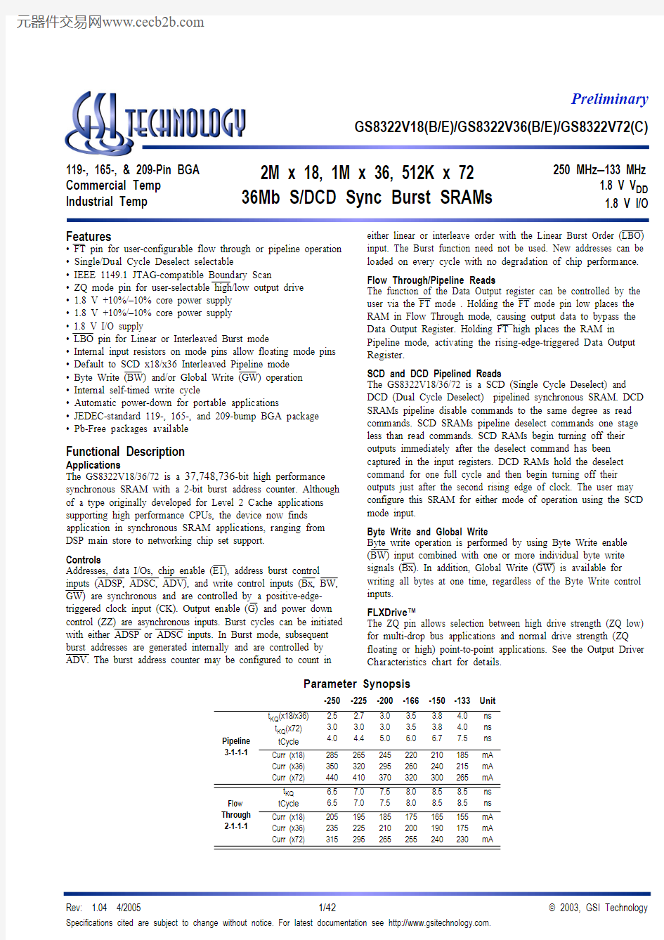
Parameter Synopsis
-250
-225-200-166-150-133Unit
Pipeline 3-1-1-1
KQ t KQ (x72)tCycle 3.04.0 3.04.4 3.05.0 3.56.0 3.86.7 4.07.5ns ns Curr (x18)Curr (x36)Curr (x72)285350440265320410245295370220260320210240300185215265mA mA mA Flow Through 2-1-1-1
t KQ tCycle 6.56.57.07.07.57.58.08.08.58.58.58.5ns ns Curr (x18)Curr (x36)Curr (x72)
205235315
195225295
185210265
175200255
165190240
155175230
mA mA mA
GS8322V18(B/E)/GS8322V36(B/E)/GS8322V72(C)
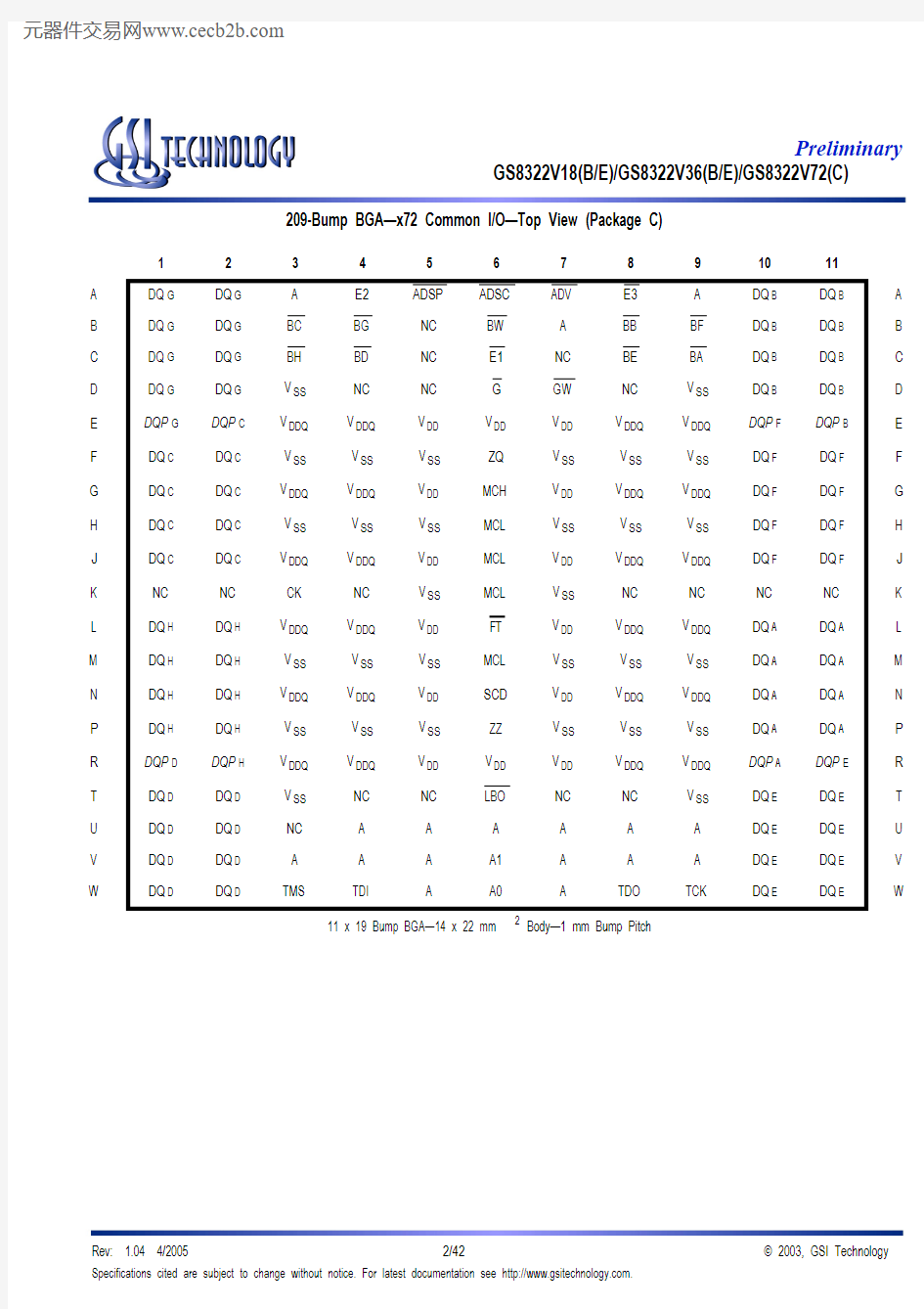
209-Bump BGA—x72 Common I/O—Top View (Package C)
1234567891011
A DQ G DQ G A E2ADSP ADSC ADV E3A DQ
B DQ B A
B DQ G DQ G B
C BG NC BW A BB BF DQ B DQ B B
C DQ G DQ G BH B
D NC E1NC B
E BA DQ B DQ B C
D DQ G DQ G V SS NC NC G GW NC V SS DQ B DQ B D
E DQP G DQP C V DDQ V DDQ V DD V DD V DD V DDQ V DDQ DQP
F DQP B E
F DQ C DQ C V SS V SS V SS ZQ V SS V SS V SS DQ F DQ F F
G DQ C DQ C V DDQ V DDQ V DD MCH V DD V DDQ V DDQ DQ F DQ F G
H DQ C DQ C V SS V SS V SS MCL V SS V SS V SS DQ F DQ F H J DQ C DQ C V DDQ V DDQ V DD MCL V DD V DDQ V DDQ DQ F DQ F J K NC NC CK NC V SS MCL V SS NC NC NC NC K L DQ H DQ H V DDQ V DDQ V DD FT V DD V DDQ V DDQ DQ A DQ A L M DQ H DQ H V SS V SS V SS MCL V SS V SS V SS DQ A DQ A M N DQ H DQ H V DDQ V DDQ V DD SCD V DD V DDQ V DDQ DQ A DQ A N P DQ H DQ H V SS V SS V SS ZZ V SS V SS V SS DQ A DQ A P R DQP D DQP H V DDQ V DDQ V DD V DD V DD V DDQ V DDQ DQP A DQP E R T DQ D DQ D V SS NC NC LBO NC NC V SS DQ E DQ E T U DQ D DQ D NC A A A A A A DQ E DQ E U V DQ D DQ D A A A A1A A A DQ E DQ E V W DQ D DQ D TMS TDI A A0A TDO TCK DQ E DQ E W
11 x 19 Bump BGA—14 x 22 mm2 Body—1 mm Bump Pitch
GS8322V18(B/E)/GS8322V36(B/E)/GS8322V72(C)
GS8322V72 209-Bump BGA Pin Description
Symbol
Type
Description
A 0, A 1I Address field LSBs and Address Counter Preset Inputs.
An I
Address Inputs
DQ A DQ B DQ C DQ D DQ E DQ F DQ G DQ H I/O Data Input and Output pins
B A , B B I Byte Write Enable for DQ A , DQ B I/Os; active low B
C ,B
D I Byte Write Enable for DQ C , DQ D I/Os; active low B
E , B
F , B
G ,B H
I Byte Write Enable for DQ E , DQ F , DQ G , DQ H I/Os; active low
NC —No Connect
CK I Clock Input Signal; active high
GW I Global Write Enable—Writes all bytes; active low
E 1I Chip Enable; active low E 3I Chip Enable; active low E 2I Chip Enable; active high G I Output Enable; active low
ADV I Burst address counter advance enable; active low ADSP, ADSC
I Address Strobe (Processor, Cache Controller); active low
ZZ I Sleep Mode control; active high FT I Flow Through or Pipeline mode; active low LBO I Linear Burst Order mode; active low
SCD I Single Cycle Deselect/Dual Cycle Deselect Mode Control
MCH I
Must Connect High MCL Must Connect Low BW I Byte Enable; active low
ZQ I FLXDrive Output Impedance Control
(Low = Low Impedance [High Drive], High = High Impedance [Low Drive])
TMS I Scan Test Mode Select TDI I Scan Test Data In TDO O Scan Test Data Out TCK
I
Scan Test Clock
GS8322V18(B/E)/GS8322V36(B/E)/GS8322V72(C)
V DD I Core power supply V SS I I/O and Core Ground V DDQ
I
Output driver power supply
GS8322V72 209-Bump BGA Pin Description (Continued)
Symbol
Type
Description
GS8322V18(B/E)/GS8322V36(B/E)/GS8322V72(C)
165-Bump BGA—x18 Commom I/O—Top View (Package E)
1234567891011
A NC A E1B
B N
C E3BW ADSC ADV A A A
B N
C A E2NC BA CK GW G ADSP A NC B
C NC NC V DDQ V SS V SS V SS V SS V SS V DDQ NC DQPA C
D NC DQB V DDQ V DD V SS V SS V SS V DD V DDQ NC DQA D
E NC DQB V DDQ V DD V SS V SS V SS V DD V DDQ NC DQA E
F NC DQB V DDQ V DD V SS V SS V SS V DD V DDQ NC DQA F
G NC DQB V DDQ V DD V SS V SS V SS V DD V DDQ NC DQA G
H FT MCL NC V DD V SS V SS V SS V DD NC ZQ ZZ H
J DQB NC V DDQ V DD V SS V SS V SS V DD V DDQ DQA NC J
K DQB NC V DDQ V DD V SS V SS V SS V DD V DDQ DQA NC K
L DQB NC V DDQ V DD V SS V SS V SS V DD V DDQ DQA NC L
M DQB NC V DDQ V DD V SS V SS V SS V DD V DDQ DQA NC M
N DQPB SCD V DDQ V SS NC A NC V SS V DDQ NC NC N
P NC NC A A TDI A1TDO A A A A P
R LBO A A A TMS A0TCK A A A A R
11 x 15 Bump BGA—15 mm x 17 mm Body—1.0 mm Bump Pitch
GS8322V18(B/E)/GS8322V36(B/E)/GS8322V72(C)
165-Bump BGA—x36 Common I/O—Top View 1
234567891011A NC A E1BC BB E3BW ADSC ADV A NC A B NC A E2BD BA CK GW G ADSP A NC B C DQPC NC V DDQ V SS V SS V SS V SS V SS V DDQ NC DQPB C D DQC DQC V DDQ V DD V SS V SS V SS V DD V DDQ DQB DQB D E DQC DQC V DDQ V DD V SS V SS V SS V DD V DDQ DQB DQB E F DQC DQC V DDQ V DD V SS V SS V SS V DD V DDQ DQB DQB F G DQC DQC V DDQ V DD V SS V SS V SS V DD V DDQ DQB DQB G H FT MCL NC V DD V SS V SS V SS V DD NC ZQ ZZ H J DQD DQD V DDQ V DD V SS V SS V SS V DD V DDQ DQA DQA J K DQD DQD V DDQ V DD V SS V SS V SS V DD V DDQ DQA DQA K L DQD DQD V DDQ V DD V SS V SS V SS V DD V DDQ DQA DQA L M DQD DQD V DDQ V DD V SS V SS V SS V DD V DDQ DQA DQA M N DQPD SCD V DDQ V SS NC A NC V SS V DDQ NC DQPA N P NC NC A A TDI A1TDO A A A A P R
LBO
A
A
A
TMS
A0
TCK
A
A
A
A
R
11 x 15 Bump BGA—15 mm x 17 mm Body—1.0 mm Bump Pitch
(Package E)
GS8322V18(B/E)/GS8322V36(B/E)/GS8322V72(C)
GS8322V18/36 165-Bump BGA Pin Description
Symbol
Type
Description
A 0, A 1I Address field LSBs and Address Counter Preset Inputs
An I Address Inputs DQ A DQ B DQ C DQ D I/O Data Input and Output pins
B A , B B , B
C , B D
I Byte Write Enable for DQ A , DQ B , DQ C , DQ D I/Os; active low (x36 Version)
NC —No Connect
CK I Clock Input Signal; active high
BW I Byte Write—Writes all enabled bytes; active low GW I Global Write Enable—Writes all bytes; active low
E 1I Chip Enable; active low E 3I Chip Enable; active low E 2I Chip Enable; active high G I Output Enable; active low
ADV I Burst address counter advance enable; active l0w ADSC, ADSP
I Address Strobe (Processor, Cache Controller); active low
ZZ I Sleep mode control; active high FT I Flow Through or Pipeline mode; active low LBO I Linear Burst Order mode; active low
ZQ I FLXDrive Output Impedance Control (Low = Low Impedance [High Drive], High = High Impedance [Low
Drive])
TMS I Scan Test Mode Select TDI I Scan Test Data In TDO O Scan Test Data Out TCK I Scan Test Clock MCL —Must Connect Low
SCD —Single Cycle Deselect/Dual Cyle Deselect Mode Control
V DD I Core power supply V SS I I/O and Core Ground V DDQ
I
Output driver power supply
GS8322V18(B/E)/GS8322V36(B/E)/GS8322V72(C)
119-Bump BGA—x36 Common I/O—Top View
1
234567A V DDQ A A ADSP A A V DDQ A B NC A A ADSC A A NC B C NC A A V DD A A NC C D DQ DQP V SS ZQ V SS DQP B DQ B D E DQ DQ V SS E1V SS DQ B DQ B E F V DDQ DQ V SS G V SS DQ B V DDQ F G DQ DQ BC ADV BB DQ B DQ B G H DQ DQ V SS GW V SS DQ B DQ B H J V DDQ V DD NC V DD NC V DD V DDQ J K DQ D DQ D V SS CK V SS DQ A DQ A K L DQ D DQ D BD SCD BA DQ A DQ A L M V DDQ DQ D V SS BW V SS DQ A V DDQ M N DQ D DQ D V SS A1V SS DQ A DQ A N P DQ D DQP D V SS A0V SS DQP A DQ A P R NC A LBO V DD FT A NC R T NC NC A A A A ZZ T U
V DDQ
TMS
TDI
TCK
TDO
NC
V DDQ
U
7 x 17 Bump BGA—14 x 22 mm 2 Body—1.27 mm Bump Pitch
C C C C C C2C C C
GS8322V18(B/E)/GS8322V36(B/E)/GS8322V72(C)
119-Bump BGA—x18 Common I/O—Top View
1234567
A V DDQ A A ADSP A A V DDQ A
B N
C A A ADSC A A NC B
C NC A A V D
D A A NC C
D DQ B NC V SS ZQ V SS DQP A NC D
E NC DQ B V SS E1V SS NC DQ A E
F V DDQ NC V SS
G V SS DQ A V DDQ F
G NC DQ B BB ADV NC NC DQ A G
H DQ B NC V SS GW V SS DQ A NC H
J V DDQ V DD NC V DD NC V DD V DDQ J
K NC DQ B V SS CK V SS NC DQ A K
L DQ B NC NC SCD BA DQ A NC L
M V DDQ DQ B V SS BW V SS NC V DDQ M
N DQ B NC V SS A1V SS DQ A NC N
P NC DQP B V SS A0V SS NC DQ A P
R NC A LBO V DD FT A NC R
T NC A A A A A ZZ T
U V DDQ TMS TDI TCK TDO NC V DDQ U
7 x 17 Bump BGA—14 x 22 mm2 Body—1.27 mm Bump Pitch
GS8322V18(B/E)/GS8322V36(B/E)/GS8322V72(C)
GS8322V18/36 119-Bump BGA Pin Description
Symbol
Type
Description
A 0, A 1I Address field LSBs and Address Counter Preset Inputs
An I Address Inputs DQ A DQ B DQ C DQ D I/O Data Input and Output pins
B A , B B , B
C , B D
I Byte Write Enable for DQ A , DQ B , DQ C , DQ D I/Os; active low
NC —No Connect
CK I Clock Input Signal; active high
BW I Byte Write—Writes all enabled bytes; active low GW I Global Write Enable—Writes all bytes; active low
E 1I Chip Enable; active low G I Output Enable; active low
ADV I Burst address counter advance enable; active low ADSP, ADSC
I Address Strobe (Processor, Cache Controller); active low
ZZ I Sleep mode control; active high FT I Flow Through or Pipeline mode; active low LBO I Linear Burst Order mode; active low
ZQ I FLXDrive Output Impedance Control (Low = Low Impedance [High Drive], High = High Impedance [Low
Drive])
SCD I Single Cycle Deselect/Dual Cyle Deselect Mode Control
TMS I Scan Test Mode Select TDI I Scan Test Data In TDO O Scan Test Data Out TCK I Scan Test Clock V DD I Core power supply V SS I I/O and Core Ground V SS I I/O and Core Ground V DDQ
I
Output driver power supply
GS8322V18(B/E)/GS8322V36(B/E)/GS8322V72(C)
A1
A0
A0A1
D0
D1Q1Q0
Counter Load
D Q
D
Q
Register
Register
D
Q
Register
D
Q
Register
D
Q
Register
D Q
Register
D Q
Register
D Q
Register
D
Q
R e g i s t e r
D
Q
Register
A0–An LBO ADV CK ADSC ADSP GW BW E 1
FT G
ZZ
Power Down Control
Memory Array
36
36
4
A
Q
D DQx1–DQx9
36
36
Note: Only x36 version shown for simplicity.
SCD
36
36
B A
B B
B C
B D
GS8322V18/36 Block Diagram
Mode Pin Functions
Mode Name
Pin Name
State
Function
Burst Order Control LBO L Linear Burst H Interleaved Burst Output Register Control FT L Flow Through H or NC Pipeline Power Down Control ZZ L or NC Active H Standby, I DD = I SB Single/Dual Cycle Deselect Control SCD L Dual Cycle Deselect H or NC Single Cycle Deselect FLXDrive Output Impedance Control
ZQ
L High Drive (Low Impedance)H or NC
Low Drive (High Impedance)
GS8322V18(B/E)/GS8322V36(B/E)/GS8322V72(C)
Note:
There are pull-up devices on the ZQ, SCD, and FT pins and a pull-down device on the ZZ pin, so those input pins can be unconnected and the chip will operate in the default states as specified in the above tables.
The burst counter wraps to initial state on the 5th clock.The burst counter wraps to initial state on the 5th clock.
Linear Burst Sequence
A[1:0]A[1:0]A[1:0]A[1:0]
1st address 000110112nd address 011011003rd address 101100014th address
11
00
01
10
I nterleaved Burst Sequence
A[1:0]A[1:0]A[1:0]A[1:0]
1st address 000110112nd address 010011103rd address 101100014th address
11
10
01
00
Burst Counter Sequences
BPR 1999.05.18
GS8322V18(B/E)/GS8322V36(B/E)/GS8322V72(C)
Byte Write Truth Table
Function
GW
BW
B A
B B
B C
B D
Notes
Read H H X X X X 1Read H L H H H H 1Write byte a H L L H H H 2, 3Write byte b H L H L H H 2, 3Write byte c H L H H L H 2, 3, 4Write byte d H L H H H L 2, 3, 4Write all bytes H L L L L L 2, 3, 4
Write all bytes
L
X
X
X
X
X
1.All byte outputs are active in read cycles regardless of the state of Byte Write Enable inputs.
2.Byte Write Enable inputs B A , B B , B C , and/or B D may be used in any combination with BW to write single or multiple bytes.
3.All byte I/Os remain High-Z during all write operations regardless of the state of Byte Write Enable inputs.
4.Bytes “C ” and “D ” are only available on the x36 version.
Synchronous Truth Table
Operation
Address Used
State Diagram Key 5
E 1
ADSP
ADSC
ADV
W 3
DQ 4
Deselect Cycle, Power Down None X H X L X X High-Z Read Cycle, Begin Burst External R L L X X X Q Read Cycle, Begin Burst External R L H L X F Q Write Cycle, Begin Burst External W L H L X T D Read Cycle, Continue Burst Next CR X H H L F Q Read Cycle, Continue Burst Next CR H X H L F Q Write Cycle, Continue Burst Next CW X H H L T D Write Cycle, Continue Burst Next CW
H X H L T D Read Cycle, Suspend Burst Current X H H H F Q Read Cycle, Suspend Burst Current H X H H F Q Write Cycle, Suspend Burst Current X H H H T D Write Cycle, Suspend Burst
Current
H
X
H
H
T
D
Notes:
1.X = Don’t Care, H = High, L = Low
2.W = T (True) and F (False) is defined in the Byte Write Truth Table preceding
3.G is an asynchronous input. G can be driven high at any time to disable active output drivers. G low can only enable active drivers (shown
as “Q” in the Truth Table above).
4.All input combinations shown above are tested and supported. Input combinations shown in gray boxes need not be used to accomplish
basic synchronous or synchronous burst operations and may be avoided for simplicity.
5.Tying ADSP high and ADSC low allows simple non-burst synchronous operations. See BOLD items above.
6.Tying ADSP high and ADV low while using ADSC to load new addresses allows simple burst operations. See ITALIC items above.
GS8322V18(B/E)/GS8322V36(B/E)/GS8322V72(C)
First Write
First Read
Burst Write
Burst Read
Deselect R W
CR
CW
X
X
W
R
R
W
R
X
X
X S i m p l e S y n c h r o n o u s O p e r a t i o n
S i m p l e B u r s t S y n c h r o n o u s O p e r a t i o n
CR R
CW
CR
CR
Notes:
1.The diagram shows only supported (tested) synchronous state transitions. The diagram presumes G is tied low.
2.The upper portion of the diagram assumes active use of only the Enable (E1) and Write (B A , B B , B C , B D , BW, and GW) control inputs, and
that ADSP is tied high and ADSC is tied low.
3.The upper and lower portions of the diagram together assume active use of only the Enable, Write, and ADSC control inputs and
assumes ADSP is tied high and ADV is tied low.
GS8322V18(B/E)/GS8322V36(B/E)/GS8322V72(C)
Simplified State Diagram
First Write
First Read
Burst Write
Burst Read
Deselect
R W
CR
CW
X
X
W
R
R
W
R
X
X
X CR
R CW CR
CR
W CW
W CW
Notes:
1.The diagram shows supported (tested) synchronous state transitions plus supported transitions that depend upon the use of G.
https://www.360docs.net/doc/e715673843.html,e of “Dummy Reads” (Read Cycles with G High) may be used to make the transition from read cycles to write cycles without passing
through a Deselect cycle. Dummy Read cycles increment the address counter just like normal read cycles.
3.Transitions shown in grey tone assume G has been pulsed high long enough to turn the RAM’s drivers off and for incoming data to meet
Data Input Set Up Time.
GS8322V18(B/E)/GS8322V36(B/E)/GS8322V72(C)
Simplified State Diagram with G
Absolute Maximum Ratings
(All voltages reference to V SS )
Symbol
Description
Value
Unit
V DD Voltage on V DD Pins –0.5 to 3.6V V DDQ Voltage in V DDQ Pins –0.5 to 3.6
V V I/O Voltage on I/O Pins –0.5 to V DDQ +0.5 (≤ 3.6 V max.)V V IN Voltage on Other Input Pins –0.5 to V DD +0.5 (≤ 3.6 V max.)
V I IN Input Current on Any Pin +/–20mA I OUT Output Current on Any I/O Pin +/–20mA P D Package Power Dissipation 1.5W
T STG Storage Temperature –55 to 125o C T BIAS
Temperature Under Bias
–55 to 125
o
C
GS8322V18(B/E)/GS8322V36(B/E)/GS8322V72(C)
Note:
Permanent damage to the device may occur if the Absolute Maximum Ratings are exceeded. Operation should be restricted to Recommended Operating Conditions. Exposure to conditions exceeding the Absolute Maximum Ratings, for an extended period of time, may affect reliability of this component. Power Supply Voltage Ranges
Parameter
Symbol
Min.
Typ.
Max.
Unit
Notes
1.8 V Supply Voltage V DD 1.6 1.8
2.0V 1.8 V V DDQ I/O Supply Voltage
V DDQ
1.6
1.8
2.0
V
Notes:
1.The part numbers of Industrial Temperature Range versions end the character “I”. Unless otherwise noted, all performance specifica-tions quoted are evaluated for worst case in the temperature range marked on the device.
2.Input Under/overshoot voltage must be –2 V > Vi < V DDn +2 V not to exceed
3.6 V maximum, with a pulse width not to exceed 20% tKC.
Recommended Operating Temperatures
Parameter
Symbol
Min.
Typ.
Max.
Unit
Notes
Ambient Temperature (Commercial Range Versions)T A 02570°C 2Ambient Temperature (Industrial Range Versions)
T A
–40
25
85
°C
2
Notes:
1.The part numbers of Industrial Temperature Range versions end the character “I”. Unless otherwise noted, all performance specifica-tions quoted are evaluated for worst case in the temperature range marked on the device.
2.Input Under/overshoot voltage must be –2 V > Vi < V DDn +2 V not to exceed 4.6 V maximum, with a pulse width not to exceed 20% tKC.
GS8322V18(B/E)/GS8322V36(B/E)/GS8322V72(C)
Logic Levels
Parameter
Symbol
Min.
Typ.
Max.
Unit
Notes
V DD Input High Voltage V IH 0.6*V DD —V DD + 0.3V 1V DD Input Low Voltage V IL –0.3—0.3*V DD V 1V DDQ I/O Input High Voltage V IHQ 0.6*V DD —V DDQ + 0.3V 1,3V DDQ I/O Input Low Voltage
V ILQ
–0.3
—
0.3*V DD
V
1,3
Notes:
1.The part numbers of Industrial Temperature Range versions end the character “I”. Unless otherwise noted, all performance specifica-tions quoted are evaluated for worst case in the temperature range marked on the device.
2.Input Under/overshoot voltage must be –2 V > Vi < V DDn +2 V not to exceed
3.6 V maximum, with a pulse width not to exceed 20% tKC.3.V IHQ (max) is voltage on V DDQ pins plus 0.3 V.
20% tKC
V SS – 2.0 V
50%V SS V IH
Undershoot Measurement and Timing
Overshoot Measurement and Timing
20% tKC
V DD + 2.0 V
50%V DD
V IL
Capacitance
o C, f = 1 MH Z , V DD Parameter
Symbol
Test conditions
Typ.
Max.
Unit
Input Capacitance C IN V IN = 0 V 45pF Input/Output Capacitance C I/O
V OUT = 0 V
6
7
pF
Note:
These parameters are sample tested.
(T A = 25= 2.5 V)
AC Test Conditions
Parameter
Conditions
Input high level V DD – 0.2 V Input low level 0.2 V Input slew rate 1 V/ns Input reference level V DD /2Output reference level
V DDQ /2Output load
Fig. 1
1.Include scope and jig capacitance.
2.Test conditions as specified with output loading as shown in Fig. 1
unless otherwise noted.
3.Device is deselected as defined by the Truth Table. GS8322V18(B/E)/GS8322V36(B/E)/GS8322V72(C)
DQ
V DDQ/2
50?30pF *
Output Load 1
* Distributed Test Jig Capacitance
DC Electrical Characteristics
Parameter
Symbol
Test Conditions
Min
Max
Input Leakage Current (except mode pins)I IL V IN = 0 to V DD –1 uA 1 uA ZZ Input Current I IN1V DD ≥ V IN ≥ V IH 0 V ≤ V IN ≤ V IH –1 uA –1 uA 1 uA 100 uA FT, SCD, and ZQ Input Current I IN2V DD ≥ V IN ≥ V IL 0 V ≤ V IN ≤ V IL
–100 uA –1 uA 1 uA 1 uA Output Leakage Current I OL Output Disable, V OUT = 0 to V DD –1 uA 1 uA Output High Voltage V OH1I OH = –4 mA, V DDQ = 1.6 V V DDQ – 0.4 V
—Output Low Voltage
V OL1
I OL = 4 mA, V DD = 1.6 V
—
0.4 V
GS8322V18(B/E)/GS8322V36(B/E)/GS8322V72(C)
r a t i n g C u r r e n t s
a m e t e r T e s t C o n d i t i o n s M o d e
S y m b o l -250
-225
-200-166-150-133
U n i t
0t o 70°C –40 t o 85°C
0t o 70°C
–40 t o 85°C 0t o 70°C –40t o 85°C 0 t o 70°C –40t o 85°C 0 t o 70°C –40t o 85°C 0 t o 70°C –40t o 85°C e r a t i n g u r r e n t
D e v i c e S e l e c t e d ; A l l o t h e r i n p u t s ≥V I H o r ≤ V I L
O u t p u t o p e n
(x 72)
P i p e l i n e
I D D
I D D Q
38060
40060
35060
370603205034050280403004026040280402353025530
m A
F l o w T h r o u g h
I D D
I D D Q
27540
28540
25540
265402353024530225302353021030220302102022020
m A
(x 36)
P i p e l i n e
I D D
I D D Q
30050
32050
27545
295452554027540225352453521030230301902521025
m A
F l o w T h r o u g h
I D D
I D D Q
21025
22025
20025
2102519020200201802019020170201802016015
17015
m A
(x 18)
P i p e l i n e
I D D
I D D Q
26025
28025
24025
26025225202452020020220201902021020
17015
19015
m A
F l o w T h r o u g h
I D D
I D D Q
19015
20015
18015
190151701518015160151701515015
16015
14015
15015
m A
t a n d b y u r r e n t
Z Z ≥ V D D – 0.2 V
—
P i p e l i n e
I S B 60
80
60
8060806080
60
80
60
80
m A
F l o w T h r o u g h
I S B
60
80
60
80608060
80
60
80
60
80
m A
s e l e c t u r r e n t
D e v i c e D e s e l e c t e d ; A l l o t h e r i n p u t s ≥ V I H o r ≤ V I L
—
P i p e l i n e
I D D
100
115
95
11090105
85
100
85
100
80
95
m A
F l o w T h r o u g h
I D D
85
100
851008095
80
95
75
90
70
85
m A
s : I D D a n d I D D Q a p p l y t o a n y c o m b i n a t i o n o f V D D 3, V D D 2, V D D Q 3, a n d V D D Q 2 o p e r a t i o n .A l l p a r a m e t e r s l i s t e d a r e w o r s t c a s e s c e n a r i o .