DTS3402进口MOS管方案
N-Channel 30-V (D-S) MOSFET
FEATURES
?Halogen-free According to IEC 61249-2-21Definition
?TrenchFET ? Power MOSFET ?100 % R g Tested
?Compliant to RoHS Directive 2002/95/EC
APPLICATIONS
?DC/DC Converter
PRODUCT SUMMARY
V DS (V)R DS(on) (Ω)I D (A)
a Q g (Typ.)30
0.058 at V GS = 10 V 3.6 2.1 nC
0.073 at V GS = 4.5 V
3.6
a.Package limited
b.Surface Mounted on 1" x 1" FR4 board.
c.t = 5 s.
d.Maximum under steady state conditions is 130 °C/W.
ABSOLUTE MAXIMUM RATINGS T A = 25 °C, unless otherwise noted
Parameter
Symbol Limit Unit Drain-Source Voltage V DS 30
V
Gate-Source Voltage
V GS ± 20
Continuous Drain Current (T J = 150 °C)T C = 25 °C I D
3.6a A T C = 70 °C 3.3
T A = 25 °C 3.3
T A = 70 °C
2.7
Pulsed Drain Current
I DM 15
Continuous Source-Drain Diode Current
T C = 25 °C I S
1.4
T A = 25 °C 0.9b, c Maximum Power Dissipation
T C = 25 °C P D 1.7W
T C = 70 °C
1.1
T A = 25 °C 1.1b, c T A = 70 °C
0.7b, c
Operating Junction and Storage T emperature Range T J , T stg - 55 to 150
°C
Soldering Recommendations (Peak Temperature)d, e 260
THERMAL RESISTANCE RATINGS
Parameter
Symbol Typical Maximum Unit
Maximum Junction-to-Ambient
b, d
t ≤ 5 s R thJA 90115°C/W
Maximum Junction-to-Foot (Drain)Steady State R thJF
6075
Notes:
a.Pulse test; pulse width ≤ 300 μs, duty cycle ≤ 2 %
b.Guaranteed by design, not subject to production testing.
Stresses beyond those listed under “Absolute Maximum Ratings” may cause permanent damage to the device. These are stress ratings only, and functional operation of the device at these or any other conditions beyond those indicated in the operational sections of the specifications is not implied. Exposure to absolute maximum rating conditions for extended periods may affect device reliability.
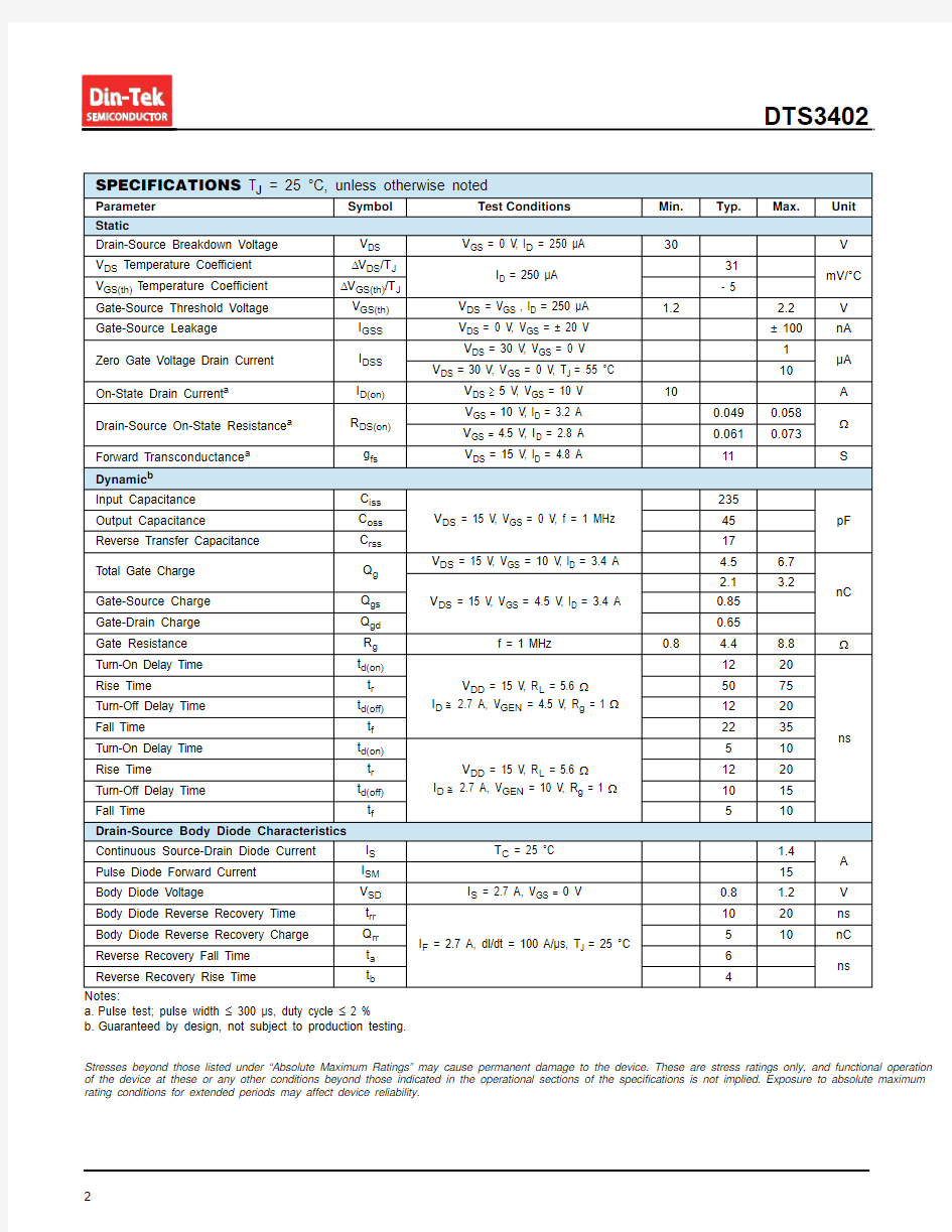
SPECIFICATIONS T J = 25 °C, unless otherwise noted
Parameter Symbol Test Conditions Min. Typ.Max.Unit
Static
Drain-Source Breakdown Voltage V DS V GS = 0 V , I D = 250 μA
30
V V DS Temperature Coefficient ΔV DS /T J I D = 250 μA
31mV/°C V GS(th) T emperature Coefficient ΔV GS(th)/T J - 5
Gate-Source Threshold Voltage V GS(th)V DS = V GS , I D = 250 μA 1.2 2.2V Gate-Source Leakage
I GSS V DS = 0 V , V GS = ± 20 V ± 100nA Zero Gate Voltage Drain Current I DSS V DS = 30 V , V GS = 0 V 1μA V DS = 30 V, V GS = 0 V , T J = 55 °C
10
On-State Drain Current a
I D(on)V DS ≥ 5 V , V GS = 10 V 10
A Drain-Source On-State Resistance a R DS(on)V GS = 10 V , I D = 3.2 A 0.0490.058ΩV GS = 4.5 V, I D = 2.8 A 0.0610.073
Forward T ransconductance a g fs
V DS = 15 V , I D = 4.8 A
11
S
Dynamic b
Input Capacitance C iss V DS = 15 V , V GS = 0 V , f = 1 MHz
235pF
Output Capacitance
C oss 45Reverse Transfer Capacitance C rss 17Total Gate Charge Q g V DS = 15 V , V GS = 10 V , I
D = 3.4 A 4.5 6.7nC V DS = 15 V , V GS = 4.5 V , I D = 3.4 A 2.1 3.2
Gate-Source Charge Q gs 0.85Gate-Drain Charge Q gd 0.65Gate Resistance R g f = 1 MHz
0.8
4.48.8Ω
Turn-On Delay Time t d(on) V DD = 15 V , R L = 5.6 Ω
I D ? 2.7 A, V GEN = 4.5 V , R g = 1 Ω
1220ns Rise Time
t r 5075Turn-Off Delay Time t d(off) 1220Fall Time
t f 2235Turn-On Delay Time t d(on) V DD = 15 V , R L = 5.6 Ω
I D ? 2.7 A, V GEN = 10 V , R g = 1 Ω510Rise Time
t r 1220Turn-Off Delay Time t d(off) 1015Fall Time
t f
5
10
Drain-Source Body Diode Characteristics Continuous Source-Drain Diode Current I S T C = 25 °C
1.4A Pulse Diode Forward Current I SM 15Body Diode Voltage
V SD I S = 2.7 A, V GS = 0 V
0.8 1.2V Body Diode Reverse Recovery Time t rr I F = 2.7 A, dI/dt = 100 A/μs, T J = 25 °C
1020ns Body Diode Reverse Recovery Charge Q rr 510
nC Reverse Recovery Fall Time t a 6ns
Reverse Recovery Rise Time
t b
4
On-Resistance vs. Drain Current and Gate Voltage
Capacitance
Single Pulse Power
TYPICAL CHARACTERISTICS 25°C, unless otherwise noted
*The power dissipation P D is based on T J(max) = 150 °C, using junction-to-case thermal resistance, and is more useful in settling the upper dissipation limit for cases where additional heatsinking is used. It is used to determine the current rating, when this rating falls below the package limit.
TYPICAL CHARACTERISTICS 25°C, unless otherwise noted
Normalized Thermal Transient Impedance, Junction-to-Ambient
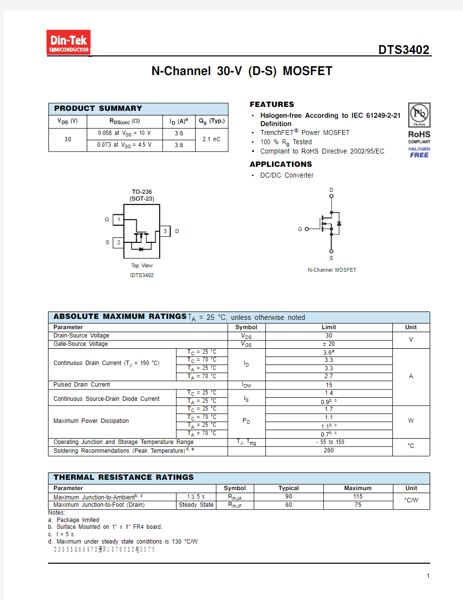
SOT-23 (TO-236): 3-LEAD
Dim
MILLIMETERS INCHES
Min
Max
Min
Max
A 0.89 1.120.0350.044A 10.010.100.00040.004A 20.88 1.020.03460.040b 0.350.500.0140.020c
0.0850.180.0030.007D 2.803.040.1100.120E 2.10 2.640.0830.104E 1 1.20
1.40
0.047
0.055
e 0.95 BSC 0.0374 Re
f e 1 1.90 BSC
0.0748 Ref
L 0.40
0.60
0.016
0.024
L 10.64 Ref 0.025 Ref S 0.50 Ref
0.020 Ref
q
3°
8°
3°
8°
ECN: S-03946-Rev. K, 09-Jul-01DWG: 5479
A P P L I C A T I O N N RECOMMENDED MINIMUM PADS FOR SOT-23
A P P L I C A T I O N N RECOMMENDED MINIMUM PADS FOR SOT-23
A P P L I C A T I O N N RECOMMENDED MINIMUM PADS FOR SOT-23
A P P L I C A T I O N N RECOMMENDED MINIMUM PADS FOR SOT-23