HLMP-CW47-PS0xx中文资料

Description
These high intensity white L ED lamps are based on InGaN material technology. A blue L ED die is coated by phosphor to produce white. The typical resulting color is described by the coordinates x = 0.31, y = 0.31using the 1931 CIE Chromaticity Diagram.
These T-1 ? lamps are untinted, diffused, and incorporate precise optics which produce well-defined spatial radiation patterns at specific viewing cone
angle.
HLMP-CW46, HLMP-CW47. HLMP-CW76, HLMP-CW77
T-1 ? (5mm) Extra Bright Precision Optical Performance White LED Lamps.
Data Sheet
Features ?Well defined spatial radiation pattern ?High luminous white emission ?Viewing angle: 50° and 70°.?Standoff or non-standoff leads ?
Superior resistance to moisture
Applications ?Electronic signs and signals ?Small area illumination ?Legend backlighting
?
General purpose indicators
Benefit
?Reduced power consumption, higher reliability, and increased optical/mechanical design flexibility compared to incandescent bulbs and other alternative white light sources.
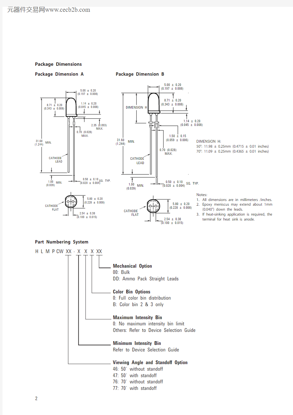
Part Numbering System
Package Dimensions Package Dimension B
Package Dimension A
Notes:
1.All dimensions are in millimeters /inches.
2.Epoxy meniscus may extend about 1mm (0.040") down the leads.
3.If heat-sinking application is required, the terminal for heat sink is anode.
Mechanical Option 00: Bulk
DD: Ammo Pack Straight Leads Color Bin Options
0: Full color bin distribution B: Color bin 2 & 3 only
Maximum Intensity Bin
0: No maximum intensity bin limit
Others: Refer to Device Selection Guide Minimum Intensity Bin
Refer to Device Selection Guide Viewing Angle and Standoff Option 46: 50? without standoff 47: 50? with standoff 76: 70? without standoff 77: 70? with standoff
H L M P --XX X X X XX
CW DIMENSION H:
50°: 11.98 ± 0.25mm (0.4715 ± 0.01 inches)70°: 11.09 ± 0.25mm (0.4365 ± 0.01 inches)
Device Selection Guide
Notes:
1.Tolerance for luminous intensity measurement is +/- 15%
2.The luminous intensity is measured on the mechanical axis of the lamp package.
3.The optical axis is closely aligned with the package mechanical axis.
4.2θ1/2 is the off-axis angle where the luminous intensity is ? the on axis intensity
5.Part numbers in BOLD are recommended for new designs.
Part Number Typical Viewing Angle,2θ ? (Degree)Intensity (mcd) at 20 MA Standoff Package Dimension Min.Max.HLMP-CW46-PS0xx 508802500No A HLMP-CW46-QR0xx 5011501900No A HLMP-CW46-QRBxx 5011501900No A HLMP-CW46-RU0xx 5015004200No A HLMP-CW46-ST0xx 5019003200No A HLMP-CW46-STBxx 5019003200No A HLMP-CW47-PS0xx 508802500Yes B HLMP-CW47-QR0xx 5011501900Yes B HLMP-CW47-QRBxx 5011501900Yes B HLMP-CW47-RU0xx 5015004200Yes B HLMP-CW47-ST0xx 5019003200Yes B HLMP-CW47-STBxx 5019003200Yes B HLMP-CW76-NR0xx 706801900No A HLMP-CW76-PQ0xx 708801500No A HLMP-CW76-PQBxx 708801500No A HLMP-CW76-QT0xx 7011503200No A HLMP-CW76-RS0xx 7015002500No A HLMP-CW76-RSBxx 7015002500No A HLMP-CW77-NR0xx 706801900Yes B HLMP-CW77-PQ0xx 708801500Yes B HLMP-CW77-PQBxx 708801500Yes B HLMP-CW77-QT0xx 7011503200Yes B HLMP-CW77-RS0xx 7015002500Yes B HLMP-CW77-RSBxx
70
1500
2500
Yes
B
AMBIENT TEMPERATURE - ?C
I F - F O R W A R D C U R R E N T - m A
Figure 3. Relative Intensity versus DC Forward Current
Figure 1. Relative Intensity vs. Wavelength
Figure 2. Forward Current vs. Ambient Temperature
Electrical/Optical Characteristics T A = 25o C
Notes:
1.The reverse voltage of the product is equivalent to the forward voltage of the protective chip at I R = 10 μA
2.The chromaticity coordinates are derived from the CIE 1931 Chromaticity Diagram and represent the perceived color of the device.
Parameters Symbol Min Typ Max Units Test Condition Forward voltage V F 3.2 4.0
V I F = 20 mA Reverse Voltage [1]V R 5.0
V
I R = 10 μA
Thermal resistance R θJ-PIN 240o
C/W
LED Junction to anode lead Chromaticity Coordinates [2]X Y 0.310.31I F = 20 mA Capacitance
C
70
V F =0, f=1MHz
0.00.20.40.60.81.0
380
480580680780
WAVELENGTH - nm
R E L A T I V E L U M I N O U S I N T E N S I T Y
0.30.60.91.21.5
0102030
FORWARD CURRENT - mA
R E L A T I V E L U M I N O U S I N T E N S I T Y
Notes:
1.Derate linearly as shown in figure
2.2.Duty factor 10%, frequency 1KHz
Absolute Maximum Rating at T A = 25o C
Parameters Value Unit DC forward current [1]
30mA Peak pulsed forward current [2]100mA Power dissipation 105mW
LED junction temperature 110o C Operating temperature range -40 to +85o C Storage temperature range
-40 to +100
o
C
Intensity Bin Limit Table
Figure 7. Spatial Radiation P attern for CW7x
Bin Intensity (mcd) at 20 mA
Min Max N 680880P 8801150Q 11501500R
15001900S 19002500T
2500
3200
U 32004200
Figure 4. Chromaticity shift vs. Current *Note: (x,y) values @ 20mA reference to (0,0)
Figure 5. Forward Current vs. Forward Voltage
Figure 6. Spatial Radiation P attern for CW4x
51015202530
2.0 2.2 2.4 2.6 2.8
3.0 3.2 3.4 3.6
V F - FORWARD VOLTAGE - VOLTS
I F - F O R W A R D C U R R E N T - m
A
X-COORDINATES
Y -C O O R D I N A T E S
00.5
1-90
-60-300306090
ANGULAR DISPLACEMENT (?)
R E L A T I V E L U M I N O U S I N T E N S I T
Y
00.5
1-90
-60
-30
30
60
90
ANGULAR DISPLACEMENT (?)
R E L A T I V E L U M I N O U S I N T E N S I T Y
Tolerance for each bin limit is ± 15%
Color Bin Limit Table
Note:
1.Bin categories are established for classification of products. Products may not be available
in all bin categories. Please contact your Avago Technologies representative for information on currently available bins.Color Bin Limits with Respect to CIE 1931 Chromaticity Diagram
Rank Limits (Chromaticity Coordinates)
1X0.3300.3300.3560.361 Y0.3600.3180.3510.385 2X0.2870.2960.3300.330 Y0.2950.2760.3180.339 3X0.2640.2800.2960.283 Y0.2670.2480.2760.305 4X0.2830.2870.3300.330 Y0.3050.2950.3390.360
Y
-
C
O
O
R
D
I
N
A
T
E
X-COORDINATE
Tolerance for each bin limit is ± 0.01
Wave Soldering Manual Solder
Dipping
Pre-heat temperature 105 °C Max.?Preheat time 30 sec Max ?
Peak temperature 250 °C Max.260 °C Max.Dwell time
3 sec Max.
5 sec Max
BOTTOM SIDE OF PC BOARD
TOP SIDE OF PC BOARD
NOTE: ALLOW FOR BOARDS TO BE SUFFICIENTLY COOLED BEFORE EXERTING MECHANICAL FORCE.
CONVEYOR SPEED = 1.83 M/MIN (6 FT/MIN)PREHEAT SETTING = 150 C (100 C PCB)SOLDER WAVE TEMPERATURE = 245 C AIR KNIFE AIR TEMPERATURE = 390 C AIR KNIFE DISTANCE = 1.91 mm (0.25 IN.)AIR KNIFE ANGLE = 40SOLDER: SN63; FLUX: RMA 250
200
150
TIME - SECONDS
T E M P E R A T U R E - ?C
100
5030
10
20
30
40
5060
70
80
90
100
LED component ead size
Diagonal Plated through hole diameter 0.457 x 0.457mm (0.018 x 0.018inch)0.646 mm (0.025 inch)0.976 to 1.078 mm (0.038 to 0.042 inch)0.508 x 0.508mm (0.020 x 0.020inch)
0.718 mm (0.028 inch)
1.049 to 1.150mm (0.041 to 0.045 inch)
Precautions:Lead Forming:
?The leads of an L ED lamp may be preformed or cut to length prior to insertion and soldering into PC board.?If lead forming is required before soldering, care must be taken to avoid any excessive mechanical stress induced to LED package. Otherwise, cut the leads of LED to length after soldering process at room temperature. The solder joint formed will absorb the mechanical stress of the lead cutting from traveling to the L ED chip die attach and wirebond.
?It is recommended that tooling made to precisely form and cut the leads to length rather than rely upon hand operation.
Soldering Condition:
?Care must be taken during PCB assembly and soldering process to prevent damage to LED component.
?The closest LED is allowed to solder on board is 1.59mm below the body (encapsulant epoxy) for those parts without standoff.
?Recommended soldering condition:
Recommended Wave Soldering Profile
Note: Refer to application note AN1027 for more information on soldering LED components.
?Wave soldering parameter must be set and maintain according to recommended temperature and dwell time in the solder wave. Customer is advised to periodically check on the soldering profile to ensure the soldering profile used is always conforming to recommended soldering condition.
?If necessary, use fixture to hold the L ED component in proper orientation with respect to the PCB during soldering process.
?Proper handling is imperative to avoid excessive thermal stresses to LED components when heated. Therefore, the soldered PCB must be allowed to cool to room temperature, 25°C before handling.
?Special attention must be given to board fabrication,solder masking, surface plating and lead holes size and component orientation to assure solderability.
?Recommended PC board plated through holes size for LED component leads.
For product information and a complete list of distributors, please go to our web site: https://www.360docs.net/doc/f87747315.html,
Avago, Avago Technologies, and the A logo are trademarks of Avago Technologies, Limited in the United States and other countries. Data subject to change. Copyright ? 2006 Avago Technologies Pte. All rights reserved.
5989-1431EN - May 29, 2006