LM2940CSX-15,LM2940CSX-15,LM2940CSX-15NOPB,LM2940CSX-15,LM2940CSX-15, 规格书,Datasheet 资料

LM2940,LM2940C
LM2940/LM2940C 1A Low Dropout Regulator
Literature Number: SNVS769H 芯天下--https://www.360docs.net/doc/fc7825642.html,/
January 2007 LM2940/LM2940C
1A Low Dropout Regulator
General Description
The LM2940/LM2940C positive voltage regulator features the
ability to source 1A of output current with a dropout voltage of
typically 0.5V and a maximum of 1V over the entire temper-
ature range. Furthermore, a quiescent current reduction cir-
cuit has been included which reduces the ground current
when the differential between the input voltage and the output
voltage exceeds approximately 3V. The quiescent current
with 1A of output current and an input-output differential of 5V
is therefore only 30 mA. Higher quiescent currents only exist
when the regulator is in the dropout mode (V
IN
? V
OUT
≤ 3V).
Designed also for vehicular applications, the LM2940/
LM2940C and all regulated circuitry are protected from re-
verse battery installations or 2-battery jumps. During line
transients, such as load dump when the input voltage can
momentarily exceed the specified maximum operating volt-
age, the regulator will automatically shut down to protect both
the internal circuits and the load. The LM2940/LM2940C can-
not be harmed by temporary mirror-image insertion. Familiar
regulator features such as short circuit and thermal overload
protection are also provided.
Features
■Dropout voltage typically 0.5V @I O = 1A
■Output current in excess of 1A
■Output voltage trimmed before assembly
■Reverse battery protection
■Internal short circuit current limit
■Mirror image insertion protection
■P+ Product Enhancement tested
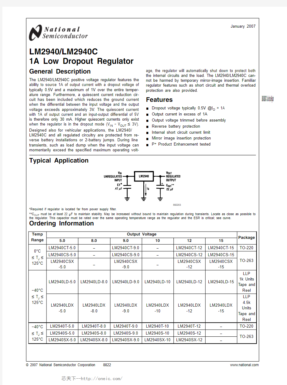
Typical Application
882203
*Required if regulator is located far from power supply filter.
**C
OUT
must be at least 22 μF to maintain stability. May be increased without bound to maintain regulation during transients. Locate as close as possible to
the regulator. This capacitor must be rated over the same operating temperature range as the regulator and the ESR is critical; see curve.
Ordering Information
Temp
Range
Output Voltage
Package
5.08.09.0101215
0°C
≤ T
J
≤
125°C
LM2940CT-5.0–LM2940CT-9.0–LM2940CT-12LM2940CT-15TO-220
LM2940CS-5.0–LM2940CS-9.0–LM2940CS-12LM2940CS-15
TO-263 LM2940CSX
-5.0
–
LM2940CSX
-9.0
–
LM2940CSX
-12
LM2940CSX
-15
?40°C
≤ T
J
≤
125°C
LM2940LD-5.0LM2940LD-8.0LM2940LD-9.0LM2940LD-10LM2940LD-12LM2940LD-15
LLP
1k Units
Tape and
Reel
LM2940LDX
-5.0
LM2940LDX
-8.0
LM2940LDX
-9.0
LM2940LDX
-10
LM2940LDX
-12
LM2940LDX
-15
LLP
4.5k
Units
Tape and
Reel ?40°C
≤ T
J
≤
125°C
LM2940T-5.0LM2940T-8.0LM2940T-9.0LM2940T-10LM2940T-12–TO-220
LM2940S-5.0LM2940S-8.0LM2940S-9.0LM2940S-10LM2940S-12–
TO-263 LM2940SX-5.0LM2940SX-8.0LM2940SX-9.0LM2940SX-10LM2940SX-12–
? 2007 National Semiconductor https://www.360docs.net/doc/fc7825642.html,
LM2940/LM2940C 1A Low Dropout Regulator
Temp
Range
Output Voltage
Package
5.08.09.0101215
?40°C
≤ T
A
≤
85°C
LM2940IMP-5.0LM2940IMP-8.0LM2940IMP-9.0LM2940IMP-10LM2940IMP-12LM2940IMP-15SOT-223
LM2940IMPX
-5.0
LM2940IMPX
-8.0
LM2940IMPX
-9.0
LM2940IMPX
-10
LM2940IMPX
-12
LM2940IMPX
-15
SOT-223
in Tape
and Reel Marking L53B L54B L0EB L55B L56B L70B The physical size of the SOT-223 is too small to contain the full device part number. The package markings indicated are what will appear on the actual device.
Mil-Aero Ordering Information
Temperature
Range
Output Voltage
Package
5.08.01215
?55°C
≤ T
J
≤
125°C
LM2940J-5.0/883
5962-8958701EA
–
LM2940J-12/883
5962-9088401QEA
LM2940J-15/883
5962-9088501QEA
J16A
LM2940WG5.0/883
5962-8958701XA
–LM2940WG5-12/883LM2940WG5-15/883WG16A For information on military temperature range products, please go to the Mil/Aero Web Site at https://www.360docs.net/doc/fc7825642.html,/appinfo/milaero/index.html.
Connection Diagrams
TO-220 (T) Plastic Package
882202
Front View
See NS Package Number TO3B
SOT-223 (MP) 3-Lead
882242
Front View
See NS Package Number MP04A
16-Lead Dual-in-Line Package (J)
882243
Top View
See NS Package Number J16A
16-Lead Ceramic Surface-Mount Package (WG)
882244
Top View
See NS Package Number WG16A TO-263 (S) Surface-Mount Package
882211
Top View
LLP (LD) 8-Lead
882246
Pin 2 and pin 7 are fused to center DAP
Pin 5 and 6 need to be tied together on PCB board
Top View
See NS Package Number LDC08A
882212
Side View
See NS Package Number TS3B
https://www.360docs.net/doc/fc7825642.html,2
L
M
2
9
4
/
L
M
2
9
4
C
Absolute Maximum Ratings (Note 1)
If Military/Aerospace specified devices are required,please contact the National Semiconductor Sales Office/Distributors for availability and specifications.LM2940S, J, WG, T, MP ≤ 100ms
60V LM2940CS, T ≤ 1 ms
45V
Internal Power Dissipation
?(Note 2)
Internally Limited
Maximum Junction Temperature 150°C Storage Temperature Range ?65°C ≤ T J ≤ +150°C
Soldering Temperature (Note 3) TO-220 (T), Wave 260°C, 10s TO-263 (S)
235°C, 30s
SOT-223 (MP)260°C, 30s LLP-8 (LD)
235°C, 30s
ESD Susceptibility (Note 4) 2 kV
Operating Conditions
(Note 1)
Input Voltage
26V
Temperature Range
LM2940T, LM2940S ?40°C ≤ T J ≤ 125°C LM2940CT, LM2940CS 0°C ≤ T J ≤ 125°C LM2940IMP
?40°C ≤ T A ≤ 85°C LM2940J, LM2940WG ?55°C ≤ T J ≤ 125°C LM2940LD
?40°C ≤ T J ≤ 125°C
Electrical Characteristics
V IN = V O + 5V, I O = 1A, C O = 22 μF, unless otherwise specified. Boldface limits apply over the entire operating temperature range of the indicated device. All other specifications apply for T A = T J = 25°C.
Output Voltage (V O )
5V 8V Units
LM2940LM2940/883
LM2940LM2940/883
Parameter Conditions
Typ
Limit Limit Typ
Limit Limit (Note 5)(Note 6) (Note 5)(Note 6)
6.25V ≤ V IN ≤ 26V 9.4V ≤ V IN ≤ 26V
Output Voltage
5 mA ≤ I O ≤ 1A
5.00 4.85/4.75 4.85/4.758.007.76/7.607.76/7.60V MIN
5.15/5.25
5.15/5.25 8.24/8.40
8.24/8.40V MAX Line Regulation
V O + 2V ≤ V IN ≤ 26V,
205040/50208050/80mV MAX
I O = 5 mA Load Regulation
50 mA ≤ I O ≤ 1A LM2940, LM2940/8833550/8050/1005580/13080/130mV MAX
LM2940C 3550 5580 Output 100 mADC and
Impedance
20 mArms,35 1000/1000
55 1000/1000
m Ω
f O = 120 Hz
Quiescent V O +2V ≤ V IN ≤ 26V, Current
I O = 5 mA
LM2940, LM2940/8831015/2015/201015/2015/20mA MAX
LM2940C 1015 V IN = V O + 5V,3045/6050/603045/6050/60mA MAX
I O = 1A
Output Noise 10 Hz ? 100 kHz,150 700/700
240 1000/1000
μV rms Voltage I O = 5 mA
Ripple Rejection
f O = 120 Hz, 1 V rms , I O = 100 mA LM29407260/54 6654/48 dB MIN
LM2940C 7260 6654 f O = 1 kHz, 1 V rms , 60/50 54/48dB MIN
I O = 5 mA
Long Term 20 32 mV/Stability
1000 Hr Dropout Voltage
I O = 1A 0.50.8/1.00.7/1.00.50.8/1.00.7/1.0V MAX
I O = 100 mA 110
150/200
150/200
110
150/200
150/200
mV MAX
https://www.360docs.net/doc/fc7825642.html,
LM2940/LM2940C
Output Voltage (V O )
5V 8V Units
LM2940LM2940/883
LM2940
LM2940/883
Parameter Conditions
Typ
Limit Limit Typ
Limit Limit
(Note 5)(Note 6) (Note 5)(Note 6)Short Circuit Current (Note 7) 1.9 1.6 1.5/1.3 1.9 1.6 1.6/1.3A MIN
Maximum Line R O = 100Ω
V MIN Transient LM2940, T ≤ 100 ms 75
60/60
75
60/60
LM2940/883, T ≤ 20 ms
40/40
40/40
LM2940C, T ≤ 1 ms 5545
5545
Reverse Polarity R O = 100Ω
DC Input Voltage
LM2940, LM2940/883?30?15/?15?15/?15
?30?15/?15?15/?15
V MIN
LM2940C ?30?15 ?30?15 Reverse Polarity R O = 100Ω
Transient Input LM2940, T ≤ 100 ms ?75?50/?50
?75?50/?50
V MIN Voltage
LM2940/883, T ≤ 20 ms ?45/?45
?45/?45
LM2940C, T ≤ 1 ms
?55
?45/?45
Electrical Characteristics
V IN = V O + 5V, I O = 1A, C O = 22 μF, unless otherwise specified. Boldface limits apply over the entire operating temperature range of the indicated device. All other specifications apply for T A = T J = 25°C.
Output Voltage (V O )
9V 10V
Units
Parameter Conditions
Typ
LM2940Typ
LM2940Limit Limit (Note 5)(Note 5)
10.5V ≤ V IN ≤ 26V 11.5V ≤ V IN ≤ 26V
Output Voltage
5 mA ≤ I O ≤1A
9.008.73/8.5510.009.70/9.50V MIN
9.27/9.45
10.30/10.50
V MAX Line Regulation
V O + 2V ≤ V IN ≤ 26V,
209020100mV MAX
I O = 5 mA Load Regulation
50 mA ≤ I O ≤ 1A LM29406090/15065100/165
mV MAX
LM2940C 6090 Output Impedance
100 mADC and
20 mArms,60 65 m Ω
f O = 120 Hz
Quiescent V O +2V ≤ V IN < 26V, Current
I O = 5 mA LM29401015/201015/20mA MAX
LM2940C
1015
V IN = V O + 5V, I O = 1A 3045/603045/60mA MAX Output Noise 10 Hz ? 100 kHz,270 300 μV rms Voltage I O = 5 mA
Ripple Rejection
f O = 120 Hz, 1 V rms ,
I O = 100 mA
LM29406452/4663
51/45
dB MIN
LM2940C
6452
Long Term Stability
34
36
mV/
1000 Hr https://www.360docs.net/doc/fc7825642.html, 4
L M 2940/L M 2940C
Output Voltage (V O )
9V 10V
Units
Parameter Conditions
Typ LM2940Typ LM2940Limit Limit (Note 5)(Note 5)Dropout Voltage I O = 1A 0.50.8/1.00.50.8/1.0V MAX I O = 100 mA 110150/200110150/200mV MAX Short Circuit (Note 7)
1.9 1.6 1.9 1.6A MIN Current Maximum Line R O = 100Ω Transient
T ≤ 100 ms LM29407560/607560/60V MIN
LM2940C 5545 Reverse Polarity R O = 100Ω DC Input Voltage
LM2940?30?15/?15?30?15/?15
V MIN
LM2940C ?30?15 Reverse Polarity R O = 100Ω Transient Input T ≤ 100 ms Voltage
LM2940?75?50/?50?75?50/?50
V MIN
LM2940C ?55
?45/?45
Electrical Characteristics
V IN = V O + 5V, I O = 1A, C O = 22 μF, unless otherwise specified. Boldface limits apply over the entire operating temperature range of the indicated device. All other specifications apply for T A = T J = 25°C.
Output Voltage (V O )
12V 15V Units
LM2940LM2940/833
LM2940LM2940/833
Parameter Conditions
Typ
Limit Limit Typ
Limit Limit (Note 5)(Note 6) (Note 5)(Note 6)
13.6V ≤ V IN ≤ 26V 16.75V ≤ V IN ≤ 26V
Output Voltage
5 mA ≤ I O ≤1A
12.0011.64/11.4011.64/11.4015.0014.55/14.2514.55/14.25V MIN
12.36/12.60
12.36/12.60 15.45/15.75
15.45/15.75V MAX Line Regulation
V O + 2V ≤ V IN ≤ 26V,
2012075/1202015095/150mV MAX
I O = 5 mA Load Regulation
50 mA ≤ I O ≤ 1A LM2940, LM2940/88355120/200120/190
150/240
mV MAX
LM2940C 55120 70150 Output 100 mADC and
Impedance
20 mArms,80 1000/1000
100 1000/1000
m Ω
f O = 120 Hz
Quiescent Current
V O +2V ≤ V IN ≤ 26V,
I O = 5 mA
LM2940, LM2940/8831015/2015/20
15/20
mA MAX
LM2940C
1015
1015
V IN = V O + 5V, I O = 1A
3045/6050/603045/6050/60mA MAX Output Noise 10 Hz ? 100 kHz,360 1000/1000
450 1000/1000
μV rms Voltage
I O = 5 mA
https://www.360docs.net/doc/fc7825642.html,
LM2940/LM2940C
Output Voltage (V O )
12V 15V Units
LM2940LM2940/833
LM2940
LM2940/833
Parameter Conditions
Typ
Limit Limit Typ
Limit Limit
(Note 5)
(Note 6)
(Note 5)
(Note 6)
Ripple Rejection
f O = 120 Hz, 1 V rms ,
I O = 100 mA
LM29406654/48
dB MIN LM2940C 66
54
64
52
f O = 1 kHz, 1 V rms , 52/46 48/42dB MIN I O = 5 mA
Long Term
48 60 mV/Stability
1000 Hr Dropout Voltage
I O = 1A 0.50.8/1.00.7/1.00.50.8/1.00.7/1.0V MAX
I O = 100 mA 110150/200150/200110150/200150/200mV MAX Short Circuit (Note 7) 1.9 1.6 1.6/1.3 1.9 1.6 1.6/1.3A MIN Current
Maximum Line R O = 100Ω
Transient
LM2940, T ≤ 100 ms 7560/60 LM2940/883, T ≤ 20 ms 40/40 40/40V MIN
LM2940C, T ≤ 1 ms 5545 5545 Reverse Polarity R O = 100Ω
DC Input LM2940, LM2940/883?30?15/?15?15/?15
?15/?15
V MIN Voltage LM2940C ?30?15 ?30?15 Reverse Polarity R O = 100Ω
Transient Input LM2940, T ≤ 100 ms ?75?50/?50
Voltage
LM2940/883, T ≤ 20 ms ?45/?45
?45/?45
V MIN
LM2940C, T ≤ 1 ms
?55?45/?45
?55
?45/?45
Thermal Performance
Thermal Resistance Junction-to-Case, θ(JC)3-Lead TO-2204 °C/W
3-Lead TO-2634 Thermal Resistance
Junction-to-Ambient, θ(JA)
3-Lead TO-220 (Note 2)60 °C/W 3-Lead TO-263 (Note 2)80 SOT-223(Note 2)174 8-Lead LLP (Note 2)
35
Note 1:Absolute Maximum Ratings are limits beyond which damage to the device may occur. Operating Conditions are conditions under which the device functions but the specifications might not be guaranteed. For guaranteed specifications and test conditions see the Electrical Characteristics.
Note 2:The maximum allowable power dissipation is a function of the maximum junction temperature, T J , the junction-to-ambient thermal resistance, θJA , and the ambient temperature, T A . Exceeding the maximum allowable power dissipation will cause excessive die temperature, and the regulator will go into thermal shutdown. The value of θJA (for devices in still air with no heatsink) is 60°C/W for the TO-220 package, 80°C/W for the TO-263 package, and 174°C/W for the SOT-223 package. The effective value of θJA can be reduced by using a heatsink (see Application Hints for specific information on heatsinking). The value of θJA for the LLP package is specifically dependent on PCB trace area, trace material, and the number of layers and thermal vias. For improved thermal resistance and power dissipation for the LLP package, refer to Application Note AN-1187. It is recommended that 6 vias be placed under the center pad to improve thermal performance.
Note 3:Refer to JEDEC J-STD-020C for surface mount device (SMD) package reflow profiles and conditions. Unless otherwise stated, the temperature and time are for Sn-Pb (STD) only.
Note 4:ESD rating is based on the human body model, 100 pF discharged through 1.5 k Ω.
Note 5:All limits are guaranteed at T A = T J = 25°C only (standard typeface) or over the entire operating temperature range of the indicated device (boldface type).All limits at T A = T J = 25°C are 100% production tested. All limits at temperature extremes are guaranteed via correlation using standard Statistical Quality Control methods.
Note 6:All limits are guaranteed at T A = T J = 25°C only (standard typeface) or over the entire operating temperature range of the indicated device (boldface type).All limits are 100% production tested and are used to calculate Outgoing Quality Levels.
Note 7:Output current will decrease with increasing temperature but will not drop below 1A at the maximum specified temperature.
https://www.360docs.net/doc/fc7825642.html, 6
L M 2940/L M 2940C
Typical Performance Characteristics
Dropout Voltage
882213Dropout Voltage vs. Temperature
882214
Output Voltage vs. Temperature
882215Quiescent Current vs. Temperature
882216
Quiescent Current
882217
Quiescent Current
882218
https://www.360docs.net/doc/fc7825642.html,
LM2940/LM2940C
Line Transient Response 882219Load Transient Response
882220
Ripple Rejection 882221
Low Voltage Behavior
882225
Low Voltage Behavior 882226Low Voltage Behavior
882227
https://www.360docs.net/doc/fc7825642.html, 8
L M 2940/L M 2940C
Low Voltage Behavior
882228Low Voltage Behavior
882229
Low Voltage Behavior
882230Output at Voltage Extremes
882231
Output at Voltage Extremes
882232
Output at Voltage Extremes
882233
https://www.360docs.net/doc/fc7825642.html,
LM2940/LM2940C
Output at Voltage Extremes 882234Output at Voltage Extremes
882235
Output at Voltage Extremes 882236
Output Capacitor ESR
882206
Peak Output Current 882208Output Impedance
882222
https://www.360docs.net/doc/fc7825642.html, 10
L M 2940/L M 2940C
Maximum Power Dissipation (TO-220)
882223Maximum Power Dissipation (SOT-223)
882224
Maximum Power Dissipation (TO-263)
882210
https://www.360docs.net/doc/fc7825642.html, LM2940/LM2940C
Equivalent Schematic Diagram
882201
https://www.360docs.net/doc/fc7825642.html, 12
L M 2940/L M 2940C
Application Information
EXTERNAL CAPACITORS
The output capacitor is critical to maintaining regulator stabil-ity, and must meet the required conditions for both ESR (Equivalent Series Resistance) and minimum amount of ca-pacitance.
MINIMUM CAPACITANCE:
The minimum output capacitance required to maintain stabil-ity is 22 μF (this value may be increased without limit). Larger values of output capacitance will give improved transient re-sponse.
ESR LIMITS:
The ESR of the output capacitor will cause loop instability if it is too high or too low. The acceptable range of ESR plotted versus load current is shown in the graph below. It is essen-tial that the output capacitor meet these requirements, or oscillations can result.
Output Capacitor ESR
882206
FIGURE 1. ESR Limits
It is important to note that for most capacitors, ESR is speci-fied only at room temperature. However, the designer must ensure that the ESR will stay inside the limits shown over the entire operating temperature range for the design.
For aluminum electrolytic capacitors, ESR will increase by about 30X as the temperature is reduced from 25°C to ?40°C. This type of capacitor is not well-suited for low temperature operation.
Solid tantalum capacitors have a more stable ESR over tem-perature, but are more expensive than aluminum electrolyt-ics. A cost-effective approach sometimes used is to parallel an aluminum electrolytic with a solid Tantalum, with the total capacitance split about 75/25% with the Aluminum being the larger value.
If two capacitors are paralleled, the effective ESR is the par-allel of the two individual values. The “flatter” ESR of the Tantalum will keep the effective ESR from rising as quickly at low temperatures.
HEATSINKING
A heatsink may be required depending on the maximum pow-er dissipation and maximum ambient temperature of the ap-plication. Under all possible operating conditions, the junction
temperature must be within the range specified under Abso-lute Maximum Ratings.
To determine if a heatsink is required, the power dissipated by the regulator, P D , must be calculated.
The figure below shows the voltages and currents which are present in the circuit, as well as the formula for calculating the power dissipated in the regulator:
882237
I IN = I L + I G
P D = (V IN ? V OUT ) I L + (V IN ) I G
FIGURE 2. Power Dissipation Diagram
The next parameter which must be calculated is the maximum allowable temperature rise, T R(MAX). This is calculated by us-ing the formula:
T R(MAX) = T J(MAX) ? T A(MAX)
where: T J(MAX)is the maximum allowable junction tempera-ture, which is 125°C for commercial grade parts.
T A(MAX)is the maximum ambient temperature which
will be encountered in the https://www.360docs.net/doc/fc7825642.html,ing the calculated values for T R(MAX) and P D , the maximum allowable value for the junction-to-ambient thermal resis-tance, θ(JA), can now be found:
θ(JA) = T R(MAX) / P D
IMPORTAN T: If the maximum allowable value for θ(JA) is found to be ≥ 53°C/W for the TO-220 package, ≥ 80°C/W for the TO-263 package, or ≥ 174°C/W for the SOT-223 pack-age, no heatsink is needed since the package alone will dissipate enough heat to satisfy these requirements.
If the calculated value for θ(JA)falls below these limits, a heatsink is required.
HEATSINKING TO-220 PACKAGE PARTS
The TO-220 can be attached to a typical heatsink, or secured to a copper plane on a PC board. If a copper plane is to be used, the values of θ(JA) will be the same as shown in the next section for the TO-263.
If a manufactured heatsink is to be selected, the value of heatsink-to-ambient thermal resistance, θ(H?A), must first be calculated:
θ(H?A) = θ(JA) ? θ(C?H) ? θ(J?C)
Where: θ(J?C)is defined as the thermal resistance from the
junction to the surface of the case. A value of 3°C/W can be assumed for θ(J?C) for this cal-culation.
https://www.360docs.net/doc/fc7825642.html,
LM2940/LM2940C
θ(C?H)
is defined as the thermal resistance between the case and the surface of the heatsink. The value of θ(C?H) will vary from about 1.5°C/W to about 2.5°C/W (depending on method of at-tachment, insulator, etc.). If the exact value is unknown, 2°C/W should be assumed for θ(C ?H).
When a value for θ(H?A) is found using the equation shown, a heatsink must be selected that has a value that is less than or equal to this number.
θ(H?A) is specified numerically by the heatsink manufacturer in the catalog, or shown in a curve that plots temperature rise vs power dissipation for the heatsink.
HEATSINKING TO-263 PACKAGE PARTS
The TO-263 (“S”) package uses a copper plane on the PCB and the PCB itself as a heatsink. To optimize the heat sinking ability of the plane and PCB, solder the tab of the package to the plane.
Figure 3 shows for the TO-263 the measured values of θ(JA)for different copper area sizes using a typical PCB with 1ounce copper and no solder mask over the copper area used for heatsinking.
882238
FIGURE 3. θ(JA) vs. Copper (1 ounce) Area for the TO-263
Package As shown in the figure, increasing the copper area beyond 1square inch produces very little improvement. It should also be observed that the minimum value of θ(JA) for the TO-263package mounted to a PCB is 32°C/W.
As a design aid, Figure 4 shows the maximum allowable pow-er dissipation compared to ambient temperature for the TO-263 device. This assumes a θ(JA) of 35°C/W for 1 square inch of 1 ounce copper and a maximum junction temperature (T J ) of 125°C.
882239
FIGURE 4. Maximum Power Dissipation vs. T A for the
TO-263 Package HEATSINKING SOT-223 PACKAGE PARTS
The SOT-223 (“MP”) packages use a copper plane on the PCB and the PCB itself as a heatsink. To optimize the heat sinking ability of the plane and PCB, solder the tab of the package to the plane.
Figure 5 and Figure 6 show the information for the SOT-223package. Figure 6 assumes a θ(JA) of 74°C/W for 1 square inch of 1 ounce copper and 51°C/W for 1 square inch of 2ounce copper, with a maximum ambient temperature (T A ) of 85°C and a maximum junction temperature (T J ) of 125°C.For techniques for improving the thermal resistance and pow-er dissipation for the SOT-223 package, please refer to Ap-plication Note AN-1028.
882240
FIGURE 5. θ(JA) vs. Copper (2 ounce) Area for the SOT-223
Package
https://www.360docs.net/doc/fc7825642.html, 14
L M 2940/L M 2940C
882241
FIGURE 6. Maximum Power Dissipation vs. T
A for the
SOT-223 Package
HEATSINKING LLP PACKAGE PARTS
The value of θ
JA
for the LLP package is specifically dependent on PCB trace area, trace material, and the number of layers
and thermal vias. It is recommended that a minimum of 6
thermal vias be placed under the center pad to improve ther-
mal performance.
For techniques for improving the thermal resistance and pow-
er dissipation for the LLP package, please refer to Application
Note AN-1187.
https://www.360docs.net/doc/fc7825642.html,
LM2940/LM2940C
Physical Dimensions inches (millimeters) unless otherwise noted
3-Lead SOT-223 Package NS Package Number MP04A
16 Lead Dual-in-Line Package (J)See NS Package Number J16A
https://www.360docs.net/doc/fc7825642.html, 16
L M 2940/L M 2940C
16 Lead Surface Mount Package (WG)
See NS Package Number WG16A
3-Lead TO-220 Plastic Package (T)
NS Package Number TO3B
https://www.360docs.net/doc/fc7825642.html, LM2940/LM2940C
3-Lead TO-263 Surface Mount Package (MP)
NS Package Number TS3B
8-Lead LLP
Order Number LM2940LD-5.0, LM2940LD-8.0,
LM2940LD-9.0, LM2940LD-10,LM2940LD-12 or LM2940LD-15NS Package Number LDC08A
https://www.360docs.net/doc/fc7825642.html, 18
L M 2940/L M 2940C
LM2940/LM2940C Notes
https://www.360docs.net/doc/fc7825642.html,