LM7812(1)
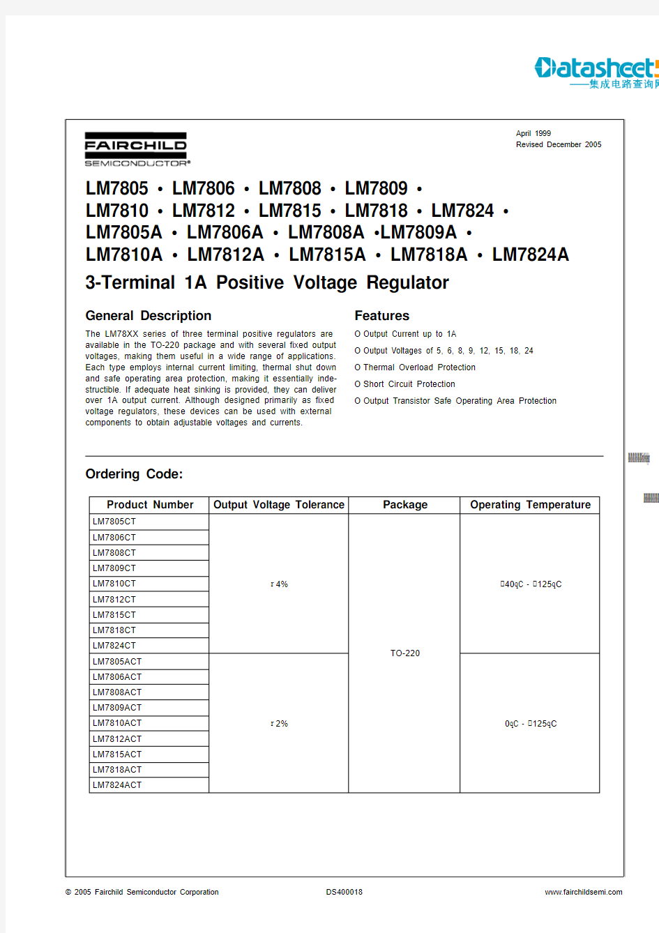
April 1999 Revised December 2005LM7805 ? LM7806 ? LM7808 ? LM7809 ? LM7810 ? LM7812 ? LM7815 ? LM7818 ? LM7824 ? LM7805A ? LM7806A ? LM7808A?LM7809A ? LM7810A ? LM7812A ? LM7815A ? LM7818A ? LM7824A 3-Terminal 1A Positive Voltage Regulator LM7805 ? LM7806 ? LM7808 ? LM7809 ? LM7810 ? LM7812 ? LM7815 ? LM7818 ? LM7824 ? LM7805A ? LM7806A ? LM7808A ?LM7809A ? LM7810A ? LM7812A ? LM7815A ? LM7818A ? LM7824A3-Terminal 1A Positive Voltage Regulator General Description The LM78XX series of three terminal positive regulators are available in the TO-220 package and with several fixed output voltages, making them useful in a wide range of applications.Each type employs internal current limiting, thermal shut down and safe operating area protection, making it essentially inde-structible. If adequate heat sinking is provided, they can deliver over 1A output current. Although designed primarily as fixed voltage regulators, these devices can be used with external components to obtain adjustable voltages and currents.Features O Output Current up to 1A O Output Voltages of 5, 6, 8, 9, 12, 15, 18, 24O Thermal Overload Protection O Short Circuit Protection O Output Transistor Safe Operating Area Protection Ordering Code:Product Number Output Voltage Tolerance Package Operating Temperature LM7805CT r4%TO-220 40q C - 125q C LM7806CT LM7808CT LM7809CT LM7810CT LM7812CT LM7815CT LM7818CT LM7824CT LM7805ACT r2%0q C - 125q C LM7806ACT LM7808ACT LM7809ACT LM7810ACT LM7812ACT LM7815ACT LM7818ACT LM7824ACT
? 2005 Fairchild Semiconductor Corporation https://www.360docs.net/doc/f015494449.html,
https://www.360docs.net/doc/f015494449.html, 2
L M 7805 ? L M 7806 ? L M 7808 ? L M 7809 ? L M 7810 ? L M 7812 ? L M 7815 ? L M 7818 ? L M 7824 ? L M 7805A ? L M 7806A ? L M 7808A ?L M 7809A ? L M 7810A ? L M 7812A ? L M 7815A ? L M 7818A ? L M 7824A
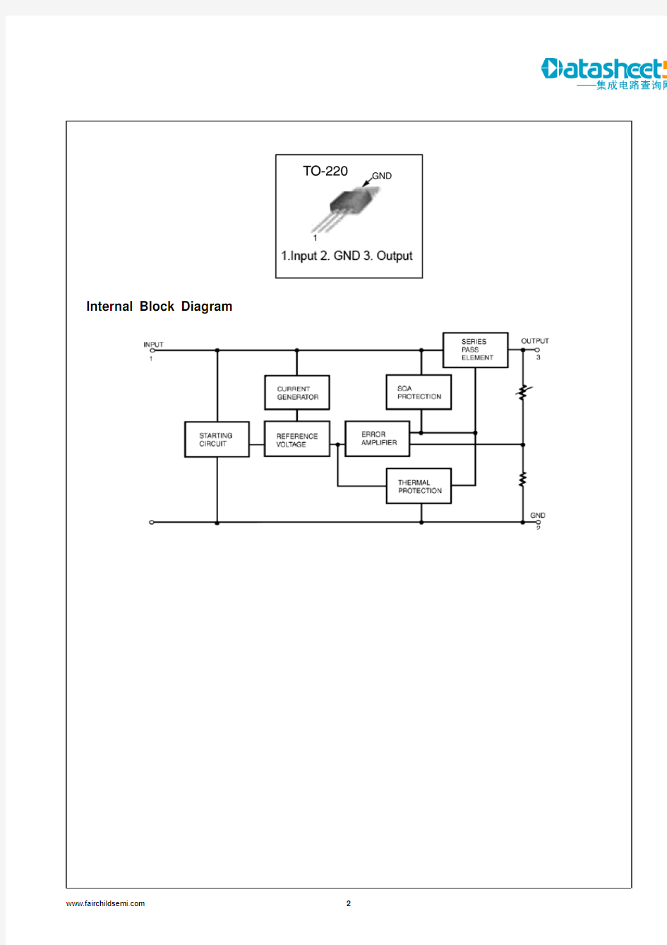
Internal Block Diagram
https://www.360docs.net/doc/f015494449.html,
LM7805 ? LM7806 ? LM7808 ? LM7809 ? LM7810 ? LM7812 ? LM7815 ? LM7818 ? LM7824 ? LM7805A ? LM7806A ? LM7808A ?LM7809A ? LM7810A ? LM7812A ? LM7815A ? LM7818A ? LM7824A
Absolute Maximum Ratings
(Note 1)
Note 1: Absolute maximum ratings are those values beyond which damage to the device may occur. The datasheet specifications should be met, without exception, to ensure that the system design is reliable over its power supply, temperature, and output/input loading variables. Fairchild does not recommend operation outside datasheet specifica-tions.
Electrical Characteristics (LM7805)
(Refer to the test circuits. 40q C T J 125q C, I O = 500mA, V I = 10V, C I = 0.1P F, unless otherwise specified)
Note 2: Load and line regulation are specified at constant junction temperature. Changes in V O due to heating effects must be taken into account separately. Pulse testing with low duty is used.
Note 3: These parameters, although guaranteed, are not 100% tested in production.
Parameter
Symbol
Value
Unit
Input Voltage (for V O = 5V to 18V)V I 35V (for V O = 24V)
V I 40V
Thermal Resistance Junction-Cases (TO-220)R T JC 5q C/W Thermal Resistance Junction-Air (TO-220)R T JA 65q C/W Operating Temperature Range T OPR
0 a 125
q C LM78xx 40 a 125q C LM78xxA
0 a 125
q C Storage Temperature Range
T STG
65 a 150
q C
Parameter
Symbol Conditions
Min Typ Max Unit Output Voltage
V O
T J = 25q C
4.8
5.0 5.2V
5mA d I O d 1A, P O d 15W, V I = 7V to 20V
4.75
5.0 5.25Line Regulation Regline
T J = 25q C
V O = 7V to 25V – 4.0100mV
(Note 2)V I = 8V to 12V – 1.650.0Load Regulation
Regload
T J = 25q C
I O = 5mA to 1.5mA –9.0100mV I O = 250mA to 750mA
– 4.050.0Quiescent Current I Q T J = 25q C – 5.08.0mA Quiescent Current Change
'I Q
I O = 5mA to 1A –0.030.5mA V I = 7V to 25V
–0.3 1.3Output Voltage Drift (Note 3)'V O /'T I O = 5mA
– 0.8–mV/q C Output Noise Voltage V N f = 10Hz to 100KHz, T A = 25q C –42.0–P V/V O Ripple Rejection (Note 3)RR f = 120Hz, V O = 8V to 18V 62.073.0–dB Dropout Voltage
V DROP I O = 1A, T J = 25q C – 2.0–V Output Resistance (Note 3)rO f = 1KHz
–15.0–m :Short Circuit Current I SC V I = 35V, T A = 25q C –230–mA Peak Current (Note 3)
I PK
T J = 25q C
–
2.2
–
A
https://www.360docs.net/doc/f015494449.html, 4
L M 7805 ? L M 7806 ? L M 7808 ? L M 7809 ? L M 7810 ? L M 7812 ? L M 7815 ? L M 7818 ? L M 7824 ? L M 7805A ? L M 7806A ? L M 7808A ?L M 7809A ? L M 7810A ? L M 7812A ? L M 7815A ? L M 7818A ? L M 7824A
Electrical Characteristics (LM7806)
(Refer to the test circuits. 40q C T J 125q C, I O = 500mA, V I = 11V, C I = 0.33P F, C O = 0.1P F, unless otherwise specified)
Note 4: Load and line regulation are specified at constant junction temperature. Changes in V O due to heating effects must be taken into account separately. Pulse testing with low duty is used.
Note 5: These parameters, although guaranteed, are not 100% tested in production.
Electrical Characteristics (LM7808)
(Refer to the test circuits. 40q C T J 125q C, I O = 500mA, V I = 14V, C I = 0.33P F, C O = 0.1P F, unless otherwise specified)
Note 6: Load and line regulation are specified at constant junction temperature. Changes in V O due to heating effects must be taken into account separately. Pulse testing with low duty is used.
Note 7: These parameters, although guaranteed, are not 100% tested in production.
Parameter
Symbol Conditions
Min Typ Max Unit Output Voltage
V O
T J = 25q C
5.75
6.0 6.25V
5mA d I O d 1A, P O d 15W, V I = 8.0V to 21V
5.7
6.0 6.3Line Regulation Regline
T J = 25q C
V I = 8V to 25V – 5.0120mV
(Note 4)V I = 9V to 13V – 1.560.0Load Regulation Regload
T J = 25q C
I O = 5mA to 1.5mA –9.0120mV (Note 4)
I O = 250mA to 750mA – 3.060.0Quiescent Current I Q T J = 25q C – 5.08.0mA Quiescent Current Change
'I Q
I O = 5mA to 1A ––0.5mA V I = 8V to 25V
–– 1.3Output Voltage Drift (Note 5)'V O /'T I O = 5mA
– 0.8–mV/q C Output Noise Voltage V N f = 10Hz to 100KHz, T A = 25q C –45.0–P V/V O Ripple Rejection (Note 5)RR f = 120Hz, V O = 8V to 18V 62.073.0–dB Dropout Voltage
V DROP I O = 1A, T J = 25q C – 2.0–V Output Resistance (Note 5)rO f = 1KHz
–19.0–m :Short Circuit Current I SC V I = 35V, T A = 25q C –250–mA Peak Current (Note 5)
I PK
T J = 25q C
–
2.2
–
A
Parameter
Symbol Conditions
Min Typ Max Unit Output Voltage
V O
T J = 25q C
7.78.08.3V
5mA d I O d 1A, P O d 15W, V I = 10.5V to 23V
7.68.08.4Line Regulation Regline
T J = 25q C
V I = 10.5V to 25V – 5.0160mV
(Note 6)V I = 11.5V to 17V – 2.080.0Load Regulation Regload
T J = 25q C
I O = 5mA to 1.5mA –10.0160mV (Note 6)
I O = 250mA to 750mA – 5.080.0Quiescent Current I Q T J = 25q C – 5.08.0mA Quiescent Current Change
'I Q
I O = 5mA to 1A –0.050.5mA V I = 10.5V to 25V
–0.5 1.0Output Voltage Drift (Note 7)'V O /'T I O = 5mA
– 0.8–mV/q C Output Noise Voltage V N f = 10Hz to 100KHz, T A = 25q C –52.0–P V/V O Ripple Rejection (Note 7)RR f = 120Hz, V O = 11.5V to 21.5V 56.073.0–dB Dropout Voltage
V DROP I O = 1A, T J = 25q C – 2.0–V Output Resistance (Note 7)rO f = 1KHz
–17.0–m :Short Circuit Current I SC V I = 35V, T A = 25q C –230–mA Peak Current (Note 7)
I PK
T J = 25q C
–
2.2
–
A
https://www.360docs.net/doc/f015494449.html,
LM7805 ? LM7806 ? LM7808 ? LM7809 ? LM7810 ? LM7812 ? LM7815 ? LM7818 ? LM7824 ? LM7805A ? LM7806A ? LM7808A ?LM7809A ? LM7810A ? LM7812A ? LM7815A ? LM7818A ? LM7824A
Electrical Characteristics (LM7809)
(Refer to the test circuits. 40q C T J 125q C, I O = 500mA, V I = 15V, C I = 0.33P F, C O = 0.1P F, unless otherwise specified)
Note 8: Load and line regulation are specified at constant junction temperature. Changes in V O due to heating effects must be taken into account separately. Pulse testing with low duty is used.
Note 9: These parameters, although guaranteed, are not 100% tested in production.
Electrical Characteristics (LM7810)
(Refer to the test circuits. 40q C T J 125q C, I O = 500mA, V I = 16V, C I = 0.33P F, C O = 0.1P F, unless otherwise specified)
Note 10: Load and line regulation are specified at constant junction temperature. Changes in V O due to heating effects must be taken into account separately. Pulse testing with low duty is used.
Note 11: These parameters, although guaranteed, are not 100% tested in production.
Parameter
Symbol Conditions
Min Typ Max Unit Output Voltage
V O
T J = 25q C
8.659.09.35V
5mA d I O d 1A, P O d 15W, V I = 11.5V to 24V
8.69.09.4Line Regulation Regline
T J = 25q C
V I = 11.5V to 25V – 6.0180mV
(Note 8)V I = 12V to 17V – 2.090.0Load Regulation Regload
T J = 25q C
I O = 5mA to 1.5mA –12.0180mV (Note 8)
I O = 250mA to 750mA – 4.090.0Quiescent Current I Q T J = 25q C – 5.08.0mA Quiescent Current Change
'I Q
I O = 5mA to 1A ––0.5mA V I = 11.5V to 26V
–– 1.3Output Voltage Drift (Note 9)'V O /'T I O = 5mA
– 1.0–mV/q C Output Noise Voltage V N f = 10Hz to 100KHz, T A = 25q C –58.0–P V/V O Ripple Rejection (Note 9)RR f = 120Hz, V O = 13V to 23V 56.071.0–dB Dropout Voltage
V DROP I O = 1A, T J = 25q C – 2.0–V Output Resistance (Note 9)rO f = 1KHz
–17.0–m :Short Circuit Current I SC V I = 35V, T A = 25q C –250–mA Peak Current (Note 9)
I PK
T J = 25q C
–
2.2
–
A
Parameter
Symbol Conditions
Min Typ Max Unit Output Voltage
V O
T J = 25q C
9.610.010.4V
5mA d I O d 1A, P O d 15W, V I = 12.5V to 25V
9.510.010.5Line Regulation Regline
T J = 25q C
V I = 12.5V to 25V –10.0200mV
(Note 10)V I = 13V to 25V – 3.0100Load Regulation Regload
T J = 25q C
I O = 5mA to 1.5mA –12.0200mV (Note 10)I O = 250mA to 750mA – 4.0400Quiescent Current I Q T J = 25q C – 5.18.0mA Quiescent Current Change
'I Q
I O = 5mA to 1A ––0.5mA V I = 12.5V to 29V
–– 1.0Output Voltage Drift (Note 11)'V O /'T I O = 5mA
– 1.0–mV/q C Output Noise Voltage V N f = 10Hz to 100KHz, T A = 25q C –58.0–P V/V O Ripple Rejection (Note 11)RR f = 120Hz, V O = 13V to 23V 56.071.0–dB Dropout Voltage
V DROP I O = 1A, T J = 25q C – 2.0–V Output Resistance (Note 11)rO f = 1KHz
–17.0–m :Short Circuit Current I SC V I = 35V, T A = 25q C –250–mA Peak Current (Note 11)
I PK
T J = 25q C
–
2.2
–
A
https://www.360docs.net/doc/f015494449.html, 6
L M 7805 ? L M 7806 ? L M 7808 ? L M 7809 ? L M 7810 ? L M 7812 ? L M 7815 ? L M 7818 ? L M 7824 ? L M 7805A ? L M 7806A ? L M 7808A ?L M 7809A ? L M 7810A ? L M 7812A ? L M 7815A ? L M 7818A ? L M 7824A
Electrical Characteristics (LM7812)
(Refer to the test circuits. 40q C T J 125q C, I O = 500mA, V I = 19V, C I = 0.33P F, C O = 0.1P F, unless otherwise specified)
Note 12: Load and line regulation are specified at constant junction temperature. Changes in V O due to heating effects must be taken into account separately. Pulse testing with low duty is used.
Note 13: These parameters, although guaranteed, are not 100% tested in production.
Electrical Characteristics (LM7815)
(Refer to the test circuits. 40q C T J 125q C, I O = 500mA, V I = 23V, C I = 0.33P F, C O = 0.1P F, unless otherwise specified)
Note 14: Load and line regulation are specified at constant junction temperature. Changes in V O due to heating effects must be taken into account separately. Pulse testing with low duty is used.
Note 15: These parameters, although guaranteed, are not 100% tested in production.
Parameter
Symbol Conditions
Min Typ Max Unit Output Voltage
V O
T J = 25q C
11.512.012.5V
5mA d I O d 1A, P O d 15W, V I = 14.5V to 27V
11.412.012.6Line Regulation Regline
T J = 25q C
V I = 14.5V to 30V –10.0240mV
(Note 12)V I = 16V to 22V – 3.0120Load Regulation Regload
T J = 25q C
I O = 5mA to 1.5mA –11.0240mV (Note 12)I O = 250mA to 750mA – 5.0120Quiescent Current I Q T J = 25q C – 5.18.0mA Quiescent Current Change
'I Q
I O = 5mA to 1A –0.10.5mA V I = 14.5V to 30V
–0.5 1.0Output Voltage Drift (Note 13)'V O /'T I O = 5mA
– 1.0–mV/q C Output Noise Voltage V N f = 10Hz to 100KHz, T A = 25q C –76.0–P V/V O Ripple Rejection (Note 13)RR f = 120Hz, V I = 15V to 25V 55.071.0–dB Dropout Voltage
V DROP I O = 1A, T J = 25q C – 2.0–V Output Resistance (Note 13)rO f = 1KHz
–18.0–m :Short Circuit Current I SC V I = 35V, T A = 25q C –230–mA Peak Current (Note 13)
I PK
T J = 25q C
–
2.2
–
A
Parameter
Symbol Conditions
Min Typ Max Unit Output Voltage
V O
T J = 25q C
14.415.015.6V
5mA d I O d 1A, P O d 15W, V I = 17.5V to 30V
14.2515.015.75Line Regulation Regline
T J = 25q C
V I = 17.5V to 30V –11.0300mV
(Note 14)V I = 20V to 26V – 3.0150Load Regulation Regload
T J = 25q C
I O = 5mA to 1.5mA –12.0300mV (Note 14)I O = 250mA to 750mA – 4.0150Quiescent Current I Q T J = 25q C – 5.28.0mA Quiescent Current Change
'I Q
I O = 5mA to 1A ––0.5mA V I = 17.5V to 30V
–– 1.0Output Voltage Drift (Note 15)'V O /'T I O = 5mA
– 1.0–mV/q C Output Noise Voltage V N f = 10Hz to 100KHz, T A = 25q C –90.0–P V/V O Ripple Rejection (Note 15)RR f = 120Hz, V I = 18.5V to 28.5V 54.070.0–dB Dropout Voltage
V DROP I O = 1A, T J = 25q C – 2.0–V Output Resistance (Note 15)rO f = 1KHz
–19.0–m :Short Circuit Current I SC V I = 35V, T A = 25q C –250–mA Peak Current (Note 15)
I PK
T J = 25q C
–
2.2
–
A
https://www.360docs.net/doc/f015494449.html,
LM7805 ? LM7806 ? LM7808 ? LM7809 ? LM7810 ? LM7812 ? LM7815 ? LM7818 ? LM7824 ? LM7805A ? LM7806A ? LM7808A ?LM7809A ? LM7810A ? LM7812A ? LM7815A ? LM7818A ? LM7824A
Electrical Characteristics (LM7818)
(Refer to the test circuits. 40q C T J 125q C, I O = 500mA, V I = 27V, C I = 0.33P F, C O = 0.1P F, unless otherwise specified)
Note 16: Load and line regulation are specified at constant junction temperature. Changes in V O due to heating effects must be taken into account separately. Pulse testing with low duty is used.
Note 17: These parameters, although guaranteed, are not 100% tested in production.
Electrical Characteristics (LM7824)
(Refer to the test circuits. 40q C T J 125q C, I O = 500mA, V I = 33V, C I = 0.33P F, C O = 0.1P F, unless otherwise specified)
Note 18: Load and line regulation are specified at constant junction temperature. Changes in V O due to heating effects must be taken into account separately. Pulse testing with low duty is used.
Note 19: These parameters, although guaranteed, are not 100% tested in production.
Parameter
Symbol Conditions
Min Typ Max Unit Output Voltage
V O
T J = 25q C
17.318.018.7V
5mA d I O d 1A, P O d 15W, V I = 21V to 33V
17.118.018.9Line Regulation Regline
T J = 25q C
V I = 21V to 33V –15.0360mV
(Note 12)V I = 24V to 30V – 5.0180Load Regulation Regload
T J = 25q C
I O = 5mA to 1.5mA –15.0360mV (Note 12)I O = 250mA to 750mA – 5.0180Quiescent Current I Q T J = 25q C – 5.28.0mA Quiescent Current Change
'I Q
I O = 5mA to 1A ––0.5mA V I = 21V to 33V
–– 1.0Output Voltage Drift (Note 17)'V O /'T I O = 5mA
– 1.0–mV/q C Output Noise Voltage V N f = 10Hz to 100KHz, T A = 25q C –110–P V/V O Ripple Rejection (Note 17)RR f = 120Hz, V I = 22V to 32V 53.069.0–dB Dropout Voltage
V DROP I O = 1A, T J = 25q C – 2.0–V Output Resistance (Note 17)rO f = 1KHz
–22.0–m :Short Circuit Current I SC V I = 35V, T A = 25q C –250–mA Peak Current (Note 17)
I PK
T J = 25q C
–
2.2
–
A
Parameter
Symbol Conditions
Min Typ Max Unit Output Voltage
V O
T J = 25q C
23.024.025.0V
5mA d I O d 1A, P O d 15W, V I = 27V to 38V
22.824.025.25Line Regulation Regline
T J = 25q C
V I = 27V to 38V –17.0480mV
(Note 18)V I = 30V to 36V – 6.0240Load Regulation Regload
T J = 25q C
I O = 5mA to 1.5mA –15.0480mV (Note 18)I O = 250mA to 750mA – 5.0240Quiescent Current I Q T J = 25q C – 5.28.0mA Quiescent Current Change
'I Q
I O = 5mA to 1A –0.10.5mA V I = 27V to 38V
–0.5 1.0Output Voltage Drift (Note 19)'V O /'T I O = 5mA
– 1.5–mV/q C Output Noise Voltage V N f = 10Hz to 100KHz, T A = 25q C –60.0–P V/V O Ripple Rejection (Note 19)RR f = 120Hz, V I = 28V to 38V 50.067.0–dB Dropout Voltage
V DROP I O = 1A, T J = 25q C – 2.0–V Output Resistance (Note 19)rO f = 1KHz
–28.0–m :Short Circuit Current I SC V I = 35V, T A = 25q C –230–mA Peak Current (Note 19)
I PK
T J = 25q C
–
2.2
–
A
https://www.360docs.net/doc/f015494449.html, 8
L M 7805 ? L M 7806 ? L M 7808 ? L M 7809 ? L M 7810 ? L M 7812 ? L M 7815 ? L M 7818 ? L M 7824 ? L M 7805A ? L M 7806A ? L M 7808A ?L M 7809A ? L M 7810A ? L M 7812A ? L M 7815A ? L M 7818A ? L M 7824A
Electrical Characteristics (LM7805A)
(Refer to the test circuits. 0q C T J 125q C, I O = 1A, V I = 10V, C I = 0.33P F, C O = 0.1P F, unless otherwise specified)
Note 20: Load and line regulation are specified at constant junction temperature. Changes in V O due to heating effects must be taken into account separately. Pulse testing with low duty is used.
Note 21: These parameters, although guaranteed, are not 100% tested in production.
Parameter
Symbol Conditions
Min Typ Max Unit Output Voltage
V O
T J = 25q C
4.9
5.0 5.1V
I O = 5mA to 1A, P O d 15W, V I = 7.5V to 20V
4.8
5.0‘ 5.2Line Regulation Regline
V I = 7.5V to 25V, I O = 500mA – 5.050.0mV (Note 20)
V I = 8V to 12V – 3.050.0T J = 25q C
V I = 7.3V to 20V – 5.050.0V I = 8V to 12V
– 1.525.0Load Regulation Regload
T J = 25q C, I O = 5mA to 1.5mA –9.0100mV (Note 20)
I O = 5mA to 1mA –9.0100I O = 250mA to 750mA
– 4.050.0Quiescent Current I Q T J = 25q C – 5.0 6.0mA Quiescent Current Change
'I Q
I O = 5mA to 1A
––0.5mA V I = 8V to 25V, I O = 500mA ––0.8V I = 7.5V to 20V, T J = 25q C
––0.8Output Voltage Drift (Note 21)'V O /'T I O = 5mA
– 0.8–mV/q C Output Noise Voltage V N f = 10Hz to 100KHz, T A = 25q C –10.0–P V/V O Ripple Rejection (Note 21)RR f = 120Hz, I O = 500mA, V I = 8V to 18V –68.0–dB Dropout Voltage
V DROP I O = 1A, T J = 25q C – 2.0–V Output Resistance (Note 21)rO f = 1KHz
–17.0–m :Short Circuit Current I SC V I = 35V, T A = 25q C –250–mA Peak Current (Note 21)
I PK
T J = 25q C
–
2.2
–
A
https://www.360docs.net/doc/f015494449.html,
LM7805 ? LM7806 ? LM7808 ? LM7809 ? LM7810 ? LM7812 ? LM7815 ? LM7818 ? LM7824 ? LM7805A ? LM7806A ? LM7808A ?LM7809A ? LM7810A ? LM7812A ? LM7815A ? LM7818A ? LM7824A
Electrical Characteristics (LM7806A)
(Refer to the test circuits. 0q C T J 125q C, I O = 1A, V I = 11V, C I = 0.33P F, C O = 0.1P F, unless otherwise specified)
Note 22: Load and line regulation are specified at constant junction temperature. Changes in V O due to heating effects must be taken into account separately. Pulse testing with low duty is used.
Note 23: These parameters, although guaranteed, are not 100% tested in production.
Parameter
Symbol Conditions
Min Typ Max Unit Output Voltage
V O
T J = 25q C
5.58
6.0 6.12V
I O = 5mA to 1A, P O d 15W, V I = 8.6V to 21V
5.76
6.0 6.24Line Regulation Regline
V I = 8.6V to 25V, I O = 500mA – 5.060.0mV (Note 22)
V I = 9V to 13V – 3.060.0T J = 25q C
V I = 8.3V to 21V – 5.060.0V I = 9V to 13V
– 1.530.0Load Regulation Regload
T J = 25q C, I O = 5mA to 1.5mA –9.0100mV (Note 22)
I O = 5mA to 1mA – 4.0100I O = 250mA to 750mA
– 5.050.0Quiescent Current I Q T J = 25q C – 4.3 6.0mA Quiescent Current Change
'I Q
I O = 5mA to 1A
––0.5mA V I = 19V to 25V, I O = 500mA ––0.8V I = 8.5V to 21V, T J = 25q C
––0.8Output Voltage Drift (Note 23)'V O /'T I O = 5mA
– 0.8–mV/q C Output Noise Voltage V N f = 10Hz to 100KHz, T A = 25q C –10.0–P V/V O Ripple Rejection (Note 23)RR f = 120Hz, I O = 500mA, V I = 9V to 19V –65.0–dB Dropout Voltage
V DROP I O = 1A, T J = 25q C – 2.0–V Output Resistance (Note 23)rO f = 1KHz
–17.0–m :Short Circuit Current I SC V I = 35V, T A = 25q C –250–mA Peak Current (Note 23)
I PK
T J = 25q C
–
2.2
–
A
https://www.360docs.net/doc/f015494449.html, 10
L M 7805 ? L M 7806 ? L M 7808 ? L M 7809 ? L M 7810 ? L M 7812 ? L M 7815 ? L M 7818 ? L M 7824 ? L M 7805A ? L M 7806A ? L M 7808A ?L M 7809A ? L M 7810A ? L M 7812A ? L M 7815A ? L M 7818A ? L M 7824A
Electrical Characteristics (LM7808A)
(Refer to the test circuits. 0q C T J 125q C, I O = 1A, V I = 14V, C I = 0.33P F, C O = 0.1P F, unless otherwise specified)
Note 24: Load and line regulation are specified at constant junction temperature. Changes in V O due to heating effects must be taken into account separately. Pulse testing with low duty is used.
Note 25: These parameters, although guaranteed, are not 100% tested in production.
Parameter
Symbol Conditions
Min Typ Max Unit Output Voltage
V O
T J = 25q C
7.848.08.16V
I O = 5mA to 1A, P O d 15W, V I = 10.6V to 23V
7.78.08.3Line Regulation Regline
V I = 10.6V to 25V, I O = 500mA – 6.080.0mV (Note 24)
V I = 11V to 17V – 3.080.0T J = 25q C
V I = 10.4V to 23V – 6.080.0V I = 11V to 17V
– 2.040.0Load Regulation Regload
T J = 25q C, I O = 5mA to 1.5mA –12.0100mV (Note 24)
I O = 5mA to 1mA –12.0100I O = 250mA to 750mA
– 5.050.0Quiescent Current I Q T J = 25q C – 5.0 6.0mA Quiescent Current Change
'I Q
I O = 5mA to 1A
––0.5mA V I = 11V to 25V, I O = 500mA ––0.8V I = 10.6V to 23V, T J = 25q C
––0.8Output Voltage Drift (Note 25)'V O /'T I O = 5mA
– 0.8–mV/q C Output Noise Voltage V N f = 10Hz to 100KHz, T A = 25q C
–10.0–P V/V O Ripple Rejection (Note 25)RR f = 120Hz, I O = 500mA, V I = 11.5V to 21.5V –62.0–dB Dropout Voltage
V DROP I O = 1A, T J = 25q C – 2.0–V Output Resistance (Note 25)rO f = 1KHz
–18.0–m :Short Circuit Current I SC V I = 35V, T A = 25q C –250–mA Peak Current (Note 25)
I PK
T J = 25q C
–
2.2
–
A
https://www.360docs.net/doc/f015494449.html,
LM7805 ? LM7806 ? LM7808 ? LM7809 ? LM7810 ? LM7812 ? LM7815 ? LM7818 ? LM7824 ? LM7805A ? LM7806A ? LM7808A ?LM7809A ? LM7810A ? LM7812A ? LM7815A ? LM7818A ? LM7824A
Electrical Characteristics (LM7809A)
(Refer to the test circuits. 0q C T J 125q C, I O = 1A, V I = 15V, C I = 0.33P F, C O = 0.1P F, unless otherwise specified)
Note 26: Load and line regulation are specified at constant junction temperature. Changes in V O due to heating effects must be taken into account separately. Pulse testing with low duty is used.
Note 27: These parameters, although guaranteed, are not 100% tested in production.
Parameter
Symbol Conditions
Min Typ Max Units Output Voltage
V O
T J = 25q C
8.829.09.16V
I O = 5mA to 1A, P O d 15W, V I = 11.2V to 24V
8.659.09.35Line Regulation Regline
V I = 11.7V to 25V, I O = 500mA – 6.090.0mV (Note 26)
V I = 12.5V to 19V – 4.045.0T J = 25q C
V I = 11.5V to 24V – 6.090.0V I = 12.5V to 19V
– 2.045.0Load Regulation Regload
T J = 25q C, I O = 5mA to 1.0mA –12.0100mV (Note 26)
I O = 5mA to 1mA –12.0100I O = 250mA to 750mA
– 5.050.0Quiescent Current I Q T J = 25q C – 5.0 6.0mA Quiescent Current Change
'I Q
I O = 5mA to 1A
––0.5mA V I = 12V to 25V, I O = 500mA ––0.8V I = 11.7V to 25V, T J = 25q C
––0.8Output Voltage Drift (Note 27)'V O /'T I O = 5mA
– 1.0–mV/q C Output Noise Voltage V N f = 10Hz to 100KHz, T A = 25q C –10.0–P V/V O Ripple Rejection (Note 27)RR f = 120Hz, I O = 500mA, V I = 12V to 22V –62.0–dB Dropout Voltage
V DROP I O = 1A, T J = 25q C – 2.0–V Output Resistance (Note 27)rO f = 1KHz
–17.0–m :Short Circuit Current I SC V I = 35V, T A = 25q C –250–mA Peak Current (Note 27)
I PK
T J = 25q C
–
2.2
–
A
https://www.360docs.net/doc/f015494449.html, 12
L M 7805 ? L M 7806 ? L M 7808 ? L M 7809 ? L M 7810 ? L M 7812 ? L M 7815 ? L M 7818 ? L M 7824 ? L M 7805A ? L M 7806A ? L M 7808A ?L M 7809A ? L M 7810A ? L M 7812A ? L M 7815A ? L M 7818A ? L M 7824A
Electrical Characteristics (LM7810A)
(Refer to the test circuits. 0q C T J 125q C, I O = 1A, V I = 16V, C I = 0.33P F, C O = 0.1P F, unless otherwise specified)
Note 28: Load and line regulation are specified at constant junction temperature. Changes in V O due to heating effects must be taken into account separately. Pulse testing with low duty is used.
Note 29: These parameters, although guaranteed, are not 100% tested in production.
Parameter
Symbol Conditions
Min Typ Max Units Output Voltage
V O
T J = 25q C
9.810.010.2V
I O = 5mA to 1A, P O d 15W, V I = 12.8V to 25V
9.610.010.4Line Regulation Regline
V I = 12.8V to 26V, I O = 500mA –8.0100mV (Note 28)
V I = 13V to 20V – 4.050.0T J = 25q C
V I = 12.5V to 25V –8.0100V I = 13V to 20V
– 3.050.0Load Regulation Regload
T J = 25q C, I O = 5mA to 1.5mA –12.0100mV (Note 28)
I O = 5mA to 1mA –12.0100I O = 250mA to 750mA
– 5.050.0Quiescent Current I Q T J = 25q C – 5.0 6.0mA Quiescent Current Change
'I Q
I O = 5mA to 1A
––0.5mA V I = 12.8V to 25V, I O = 500mA ––0.8V I = 13V to 26V, T J = 25q C
––0.5Output Voltage Drift (Note 29)'V O /'T I O = 5mA
– 1.0–mV/q C Output Noise Voltage V N f = 10Hz to 100KHz, T A = 25q C –10.0–P V/V O Ripple Rejection (Note 29)RR f = 120Hz, I O = 500mA, V I = 14V to 24V –62.0–dB Dropout Voltage
V DROP I O = 1A, T J = 25q C – 2.0–V Output Resistance (Note 29)rO f = 1KHz
–17.0–m :Short Circuit Current I SC V I = 35V, T A = 25q C –250–mA Peak Current (Note 29)
I PK
T J = 25q C
–
2.2
–
A
https://www.360docs.net/doc/f015494449.html,
LM7805 ? LM7806 ? LM7808 ? LM7809 ? LM7810 ? LM7812 ? LM7815 ? LM7818 ? LM7824 ? LM7805A ? LM7806A ? LM7808A ?LM7809A ? LM7810A ? LM7812A ? LM7815A ? LM7818A ? LM7824A
Electrical Characteristics (LM7812A)
(Refer to the test circuits. 0q C T J 125q C, I O = 1A, V I = 19V, C I = 0.33P F, C O = 0.1P F, unless otherwise specified)
Note 30: Load and line regulation are specified at constant junction temperature. Changes in V O due to heating effects must be taken into account separately. Pulse testing with low duty is used.
Note 31: These parameters, although guaranteed, are not 100% tested in production.
Parameter
Symbol Conditions
Min Typ Max Units Output Voltage
V O
T J = 25q C
11.7512.012.25V
I O = 5mA to 1A, P O d 15W, V I = 14.8V to 27V
11.512.012.5Line Regulation Regline
V I = 14.8V to 30V, I O = 500mA –10.0120mV (Note 30)
V I = 16V to 22V – 4.0120T J = 25q C
V I = 14.5V to 27V –10.0120V I = 16V to 22V
– 3.060.0Load Regulation Regload
T J = 25q C, I O = 5mA to 1.5mA –12.0100mV (Note 30)
I O = 5mA to 1mA –12.0100I O = 250mA to 750mA
– 5.050.0Quiescent Current I Q T J = 25q C – 5.1 6.0mA Quiescent Current Change
'I Q
I O = 5mA to 1A
––0.5mA V I = 14V to 27V, I O = 500mA ––0.8V I = 15V to 30V, T J = 25q C
––0.8Output Voltage Drift (Note 31)'V O /'T I O = 5mA
– 1.0–mV/q C Output Noise Voltage V N f = 10Hz to 100KHz, T A = 25q C –10.0–P V/V O Ripple Rejection (Note 31)RR f = 120Hz, I O = 500mA, V I = 14V to 24V –60.0–dB Dropout Voltage
V DROP I O = 1A, T J = 25q C – 2.0–V Output Resistance (Note 31)rO f = 1KHz
–18.0–m :Short Circuit Current I SC V I = 35V, T A = 25q C –250–mA Peak Current (Note 31)
I PK
T J = 25q C
–
2.2
–
A
https://www.360docs.net/doc/f015494449.html, 14
L M 7805 ? L M 7806 ? L M 7808 ? L M 7809 ? L M 7810 ? L M 7812 ? L M 7815 ? L M 7818 ? L M 7824 ? L M 7805A ? L M 7806A ? L M 7808A ?L M 7809A ? L M 7810A ? L M 7812A ? L M 7815A ? L M 7818A ? L M 7824A
Electrical Characteristics (LM7815A)
(Refer to the test circuits. 0q C T J 125q C, I O = 1A, V I = 23V, C I = 0.33P F, C O = 0.1P F, unless otherwise specified)
Note 32: Load and line regulation are specified at constant junction temperature. Changes in V O due to heating effects must be taken into account separately. Pulse testing with low duty is used.
Note 33: These parameters, although guaranteed, are not 100% tested in production.
Parameter
Symbol Conditions
Min Typ Max Units Output Voltage
V O
T J = 25q C
14.7515.015.3V
I O = 5mA to 1A, P O d 15W, V I = 17.7V to 30V
14.415.015.6Line Regulation Regline
V I = 17.4V to 30V, I O = 500mA –10.0150mV (Note 32)
V I = 20V to 26V – 5.0150T J = 25q C
V I = 17.5V to 30V –11.0150V I = 20V to 26V
– 3.075.0Load Regulation Regload
T J = 25q C, I O = 5mA to 1.5mA –12.0100mV (Note 32)
I O = 5mA to 1mA –12.0100I O = 250mA to 750mA
– 5.050.0Quiescent Current I Q T J = 25q C – 5.2 6.0mA Quiescent Current Change
'I Q
I O = 5mA to 1A
––0.5mA V I = 17.5V to 30V, I O = 500mA ––0.8V I = 17.5V to 30V, T J = 25q C
––0.8Output Voltage Drift (Note 33)'V O /'T I O = 5mA
– 1.0–mV/q C Output Noise Voltage V N f = 10Hz to 100KHz, T A = 25q C
–10.0–P V/V O Ripple Rejection (Note 33)RR f = 120Hz, I O = 500mA, V I = 18.5V to 28.5V –58.0–dB Dropout Voltage
V DROP I O = 1A, T J = 25q C – 2.0–V Output Resistance (Note 33)rO f = 1KHz
–19.0–m :Short Circuit Current I SC V I = 35V, T A = 25q C –250–mA Peak Current (Note 33)
I PK
T J = 25q C
–
2.2
–
A
https://www.360docs.net/doc/f015494449.html,
LM7805 ? LM7806 ? LM7808 ? LM7809 ? LM7810 ? LM7812 ? LM7815 ? LM7818 ? LM7824 ? LM7805A ? LM7806A ? LM7808A ?LM7809A ? LM7810A ? LM7812A ? LM7815A ? LM7818A ? LM7824A
Electrical Characteristics (LM7818A)
(Refer to the test circuits. 0q C T J 125q C, I O = 1A, V I = 27V, C I = 0.33P F, C O = 0.1P F, unless otherwise specified)
Note 34: Load and line regulation are specified at constant junction temperature. Changes in V O due to heating effects must be taken into account separately. Pulse testing with low duty is used.
Note 35: These parameters, although guaranteed, are not 100% tested in production.
Parameter
Symbol Conditions
Min Typ Max Units Output Voltage
V O
T J = 25q C
17.6418.018.36V
I O = 5mA to 1A, P O d 15W, V I = 21V to 33V
17.318.018.7Line Regulation Regline
V I = 21V to 33V, I O = 500mA –15.0180mV (Note 34)
V I = 21V to 33V – 5.0180T J = 25q C
V I = 20.6V to 33V –15.0180V I = 24V to 30V
– 5.090.0Load Regulation Regload
T J = 25q C, I O = 5mA to 1.5mA –15.0100mV (Note 34)
I O = 5mA to 1mA –15.0100I O = 250mA to 750mA
–7.050.0Quiescent Current I Q T J = 25q C – 5.2 6.0mA Quiescent Current Change
'I Q
I O = 5mA to 1A
––0.5mA V I = 12V to 33V, I O = 500mA ––0.8V I = 12V to 33V, T J = 25q C
––0.8Output Voltage Drift (Note 35)'V O /'T I O = 5mA
– 1.0–mV/q C Output Noise Voltage V N f = 10Hz to 100KHz, T A = 25q C –10.0–P V/V O Ripple Rejection (Note 35)RR f = 120Hz, I O = 500mA, V I = 22V to 32V –57.0–dB Dropout Voltage
V DROP I O = 1A, T J = 25q C – 2.0–V Output Resistance (Note 35)rO f = 1KHz
–19.0–m :Short Circuit Current I SC V I = 35V, T A = 25q C –250–mA Peak Current (Note 35)
I PK
T J = 25q C
–
2.2
–
A
https://www.360docs.net/doc/f015494449.html, 16
L M 7805 ? L M 7806 ? L M 7808 ? L M 7809 ? L M 7810 ? L M 7812 ? L M 7815 ? L M 7818 ? L M 7824 ? L M 7805A ? L M 7806A ? L M 7808A ?L M 7809A ? L M 7810A ? L M 7812A ? L M 7815A ? L M 7818A ? L M 7824A
Electrical Characteristics (LM7824A)
(Refer to the test circuits. 0q C T J 125q C, I O = 1A, V I = 33V, C I = 0.33P F, C O = 0.1P F, unless otherwise specified)
Note 36: Load and line regulation are specified at constant junction temperature. Changes in V O due to heating effects must be taken into account separately. Pulse testing with low duty is used.
Note 37: These parameters, although guaranteed, are not 100% tested in production.
Parameter
Symbol Conditions
Min Typ Max Units Output Voltage
V O
T J = 25q C
23.524.024.5V
I O = 5mA to 1A, P O d 15W, V I = 27.3V to 38V
23.024.025.0Line Regulation Regline
V I = 27V to 38V, I O = 500mA –18.0240mV (Note 36)
V I = 21V to 33V – 6.0240T J = 25q C
V I = 26.7V to 38V –18.0240V I = 30V to 36V
– 6.0120Load Regulation Regload
T J = 25q C, I O = 5mA to 1.5mA –15.0100mV (Note 36)
I O = 5mA to 1mA –15.0100I O = 250mA to 750mA
–7.050.0Quiescent Current I Q T J = 25q C – 5.2 6.0mA Quiescent Current Change
'I Q
I O = 5mA to 1A
––0.5mA V I = 27.3V to 38V, I O = 500mA ––0.8V I = 27.3V to 38V, T J = 25q C
––0.8Output Voltage Drift (Note 37)'V O /'T I O = 5mA
– 1.5–mV/q C Output Noise Voltage V N f = 10Hz to 100KHz, T A = 25q C –10.0–P V/V O Ripple Rejection (Note 37)RR f = 120Hz, I O = 500mA, V I = 28V to 38V –54.0–dB Dropout Voltage
V DROP I O = 1A, T J = 25q C – 2.0–V Output Resistance (Note 37)rO f = 1KHz
–20.0–m :Short Circuit Current I SC V I = 35V, T A = 25q C –250–mA Peak Current (Note 37)
I PK
T J = 25q C
–
2.2
–
A
https://www.360docs.net/doc/f015494449.html,
LM7805 ? LM7806 ? LM7808 ? LM7809 ? LM7810 ? LM7812 ? LM7815 ? LM7818 ? LM7824 ? LM7805A ? LM7806A ? LM7808A ?LM7809A ? LM7810A ? LM7812A ? LM7815A ? LM7818A ? LM7824A
Typical Performance Characteristics
FIGURE 1. Quiescent Current
FIGURE 2. Peak Output Current
FIGURE 3. Output Voltage
FIGURE 4. Quiescent Current
https://www.360docs.net/doc/f015494449.html,
18
L M 7805 ? L M 7806 ? L M 7808 ? L M 7809 ? L M 7810 ? L M 7812 ? L M 7815 ? L M 7818 ? L M 7824 ? L M 7805A ? L M 7806A ? L M 7808A ?L M 7809A ? L M 7810A ? L M 7812A ? L M 7815A ? L M 7818A ? L M 7824A
Typical Applications
FIGURE 5. DC Parameters
FIGURE 6. Load Regulation
FIGURE 7. Ripple Rejection
FIGURE 8. Fixed Output Regulator
https://www.360docs.net/doc/f015494449.html,
LM7805 ? LM7806 ? LM7808 ? LM7809 ? LM7810 ? LM7812 ? LM7815 ? LM7818 ? LM7824 ? LM7805A ? LM7806A ? LM7808A ?LM7809A ? LM7810A ? LM7812A ? LM7815A ? LM7818A ? LM7824A
Typical Applications (continued)
FIGURE 9.
Note: To specify an output voltage, substitute voltage value for “XX”. A common ground is required between the Input and the Output voltage. The input voltage must remain typ-ically 2.0V above the output voltage even during the low point on the input ripple voltage.Note: C I is required if regulator is located an appreciable distance from the power supply filter.Note: C O improves stability and transient response.
I RI t 5 I Q
V O = V XX (1 R 2 / R 1) I Q R 2
FIGURE 10. Circuit for Increasing Output Voltage
I RI t 5 I Q
V O = V XX (1 R 2 / R 1) I Q R 2
FIGURE 11. Adjustable Output Regulator (7V to 30V)
https://www.360docs.net/doc/f015494449.html, 20
L M 7805 ? L M 7806 ? L M 7808 ? L M 7809 ? L M 7810 ? L M 7812 ? L M 7815 ? L M 7818 ? L M 7824 ? L M 7805A ? L M 7806A ? L M 7808A ?L M 7809A ? L M 7810A ? L M 7812A ? L M 7815A ? L M 7818A ? L M 7824A
Typical Applications (continued)
FIGURE 12. High Current Voltage Regulator
FIGURE 13. High Output Current with Short Circuit Protection
FIGURE 14. Tracking Voltage Regulator