9972gp datasheet

N-CHANNEL ENHANCEMENT MODE POWER MOSFET
Symbol Units V DS V V GS
V I D @T C =25℃A I D @T C =100℃A I DM
A P D @T C =25℃W W/℃E AS Single Pulse Avalanche Energy 3mJ I AR A T STG ℃T J
℃
Symbol Value Units Rthj-c Maximum Thermal Resistance, Junction-case 1.4℃/W Rthj-a
Maximum Thermal Resistance, Junction-ambient
62
℃/W
Thermal Data
Parameter
Storage Temperature Range
Total Power Dissipation 89-55 to 150Operating Junction Temperature Range
-55 to 150
Linear Derating Factor
0.7Avalanche Current 3
Continuous Drain Current, V GS @ 10V 38Pulsed Drain Current 1230Gate-Source Voltage
±25Continuous Drain Current, V GS @ 10V 60Parameter
Rating Drain-Source Voltage 60RoHS-compliant Product
AP9972GS/P
30
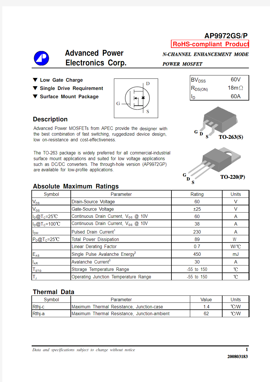
450G D
S
TO-263(S)
G D
S TO-220(P)
Electrical Characteristics@T j =25o C(unless otherwise specified)
Symbol Parameter
Test Conditions
Min.Typ.
Max.Units BV DSS
Drain-Source Breakdown Voltage V GS =0V, I D =250uA 60--V ΔB V DSS /ΔT j
Breakdown Voltage Temperature Coefficient Reference to 25℃, I D =1mA
-0.06-V/℃R DS(ON)Static Drain-Source On-Resistance 2V GS =10V, I D =35A --18m ΩV GS =4.5V, I D =25A --22m ΩV GS(th)Gate Threshold Voltage V DS =V GS , I D =250uA 1-3V g fs Forward Transconductance V DS =10V, I D =35A -55-S I DSS Drain-Source Leakage Current
V DS =60V, V GS =0V --10uA Drain-Source Leakage Current (T j =150o C)
V DS =48V ,V GS =0V --25uA I GSS Gate-Source Leakage V GS =±25V --±100nA Q g Total Gate Charge 2I D =35A -3251nC Q gs Gate-Source Charge V DS =48V -8-nC Q gd Gate-Drain ("Miller") Charge V GS =4.5V -20-nC t d(on)Turn-on Delay Time 2V DS =30V -11-ns t r Rise Time
I D =35A
-58-ns t d(off)Turn-off Delay Time R G =3.3Ω,V GS =10V -45-ns t f Fall Time R D =0.86Ω-80-ns C iss Input Capacitance V GS =0V -31705070
pF C oss Output Capacitance
V DS =25V -280-pF C rss Reverse Transfer Capacitance f=1.0MHz -230-pF R g
Gate Resistance
f=1.0MHz
-
1.7
-Ω
Source-Drain Diode
Symbol Parameter
Test Conditions
Min.Typ.Max.Units V SD
Forward On Voltage 2I S =35A, V GS =0V -- 1.2V t rr
Reverse Recovery Time 2I S =35A, V GS =0V ,-50-ns Q rr
Reverse Recovery Charge
dI/dt=100A/μs
-48
-nC
Notes:
1.Pulse width limited by Max. junction temperature.
2.Pulse width <300us , duty cycle <2%.
3.Starting T j =25o C , V DD =30V , L=1mH , R G =25Ω , I AS =30A.
THIS PRODUCT IS AN ELECTROSTATIC SENSITIVE, PLEASE HANDLE WITH CAUTION.
DEVICE OR SYSTEM ARE NOT AUTHORIZED.
THIS PRODUCT HAS BEEN QUALIFIED FOR CONSUMER MARKET. APPLICATIONS OR USES AS CRITERIAL COMPONENT IN LIFE SUPPORT
AP9972GS/P
Fig 2. Typical Output Characteristics
Fig 3. On-Resistance v.s. Gate Voltage
v.s. Junction Temperature
Fig 5. Forward Characteristic of Fig 6. Gate Threshold Voltage v.s.
Reverse Diode Junction Temperature
Fig 7. Gate Charge Characteristics Fig 8. Typical Capacitance Characteristics
Fig 9. Maximum Safe Operating Area Fig 10. Effective Transient Thermal Impedance
Fig 12. Gate Charge Waveform
AP9972GS/P