MMDT2227-7-F;中文规格书,Datasheet资料

COMPLEMENTARY NPN / PNP
SMALL SIGNAL SURFACE MOUNT TRANSISTOR
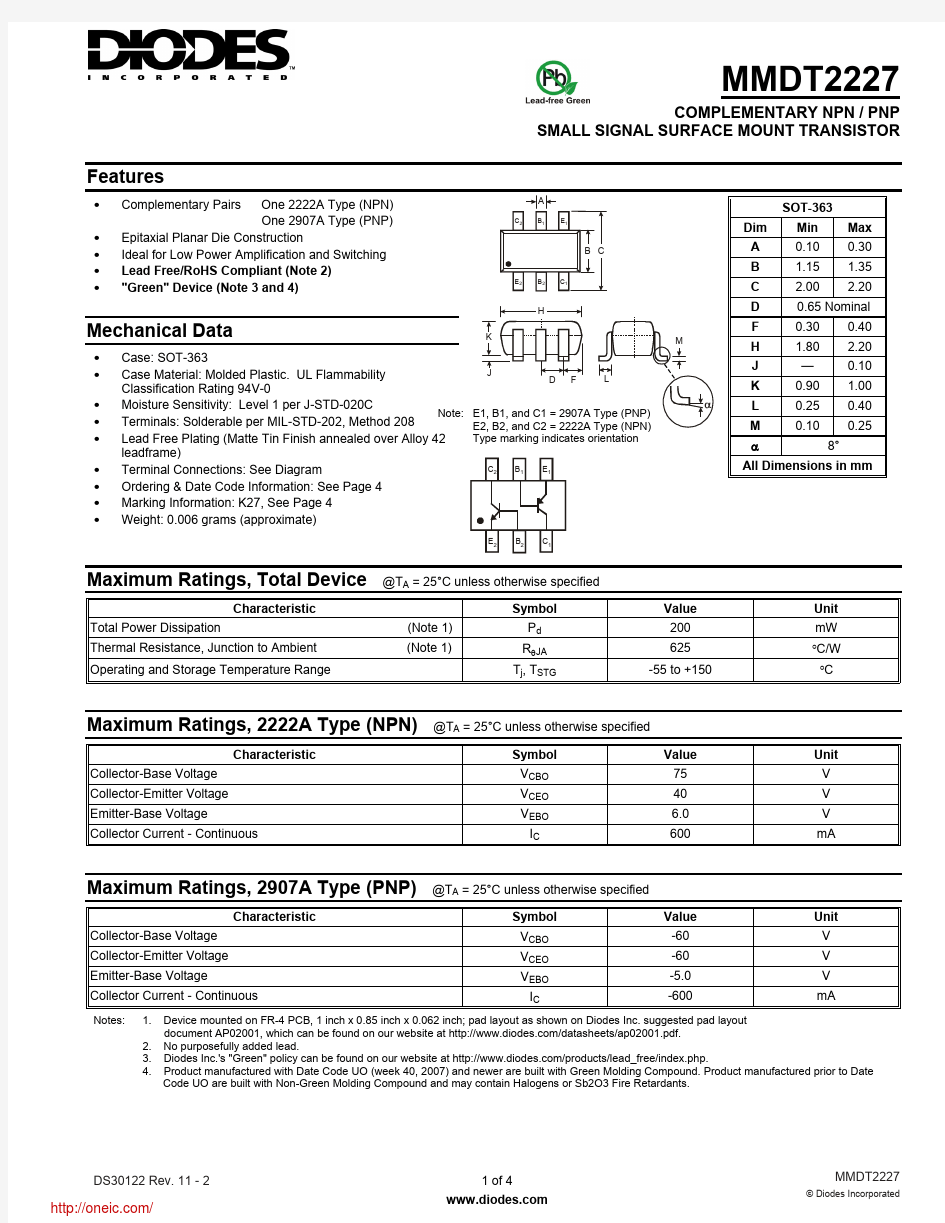
Maximum Ratings, Total Device @T A = 25°C unless otherwise specified
Characteristic Symbol Value Unit
Total Power Dissipation (Note 1) P d200 mW
Thermal Resistance, Junction to Ambient (Note 1) RθJA625 °C/W
Operating and Storage Temperature Range T j, T STG-55 to +150 °C Maximum Ratings, 2222A Type (NPN) @T A = 25°C unless otherwise specified
Characteristic Symbol Value Unit
Collector-Base Voltage V CBO75 V
Collector-Emitter Voltage V CEO40 V
Emitter-Base Voltage V EBO 6.0 V
Collector Current - Continuous I C600 mA Maximum Ratings, 2907A Type (PNP) @T A = 25°C unless otherwise specified
Characteristic Symbol Value Unit
Collector-Base Voltage V CBO-60 V
Collector-Emitter Voltage V CEO-60 V
Emitter-Base Voltage V EBO-5.0 V
Collector Current - Continuous I C-600 mA
Notes: 1. Device mounted on FR-4 PCB, 1 inch x 0.85 inch x 0.062 inch; pad layout as shown on Diodes Inc. suggested pad layout
document AP02001, which can be found on our website at https://www.360docs.net/doc/f219044150.html,/datasheets/ap02001.pdf.
2. No purposefully added lead.
3. Diodes Inc.'s "Green" policy can be found on our website at https://www.360docs.net/doc/f219044150.html,/products/lead_free/index.php.
4. Product manufactured with Date Code UO (week 40, 2007) and newer are built with Green Molding Compound. Product manufactured prior to Date Code UO are built with Non-Green Molding Compound and may contain Halogens or Sb2O3 Fire Retardants.
Electrical Characteristics, 2222A Type (NPN) @T A = 25°C unless otherwise specified
Characteristic
Symbol Min Max Unit Test Condition
OFF CHARACTERISTICS (Note 5) Collector-Base Breakdown Voltage V (BR)CBO 75 ? V I C = 10μA, I E = 0 Collector-Emitter Breakdown Voltage V (BR)CEO 40 ? V I C = 10mA, I B = 0 Emitter-Base Breakdown Voltage V (BR)EBO 6.0 ? V I E = 10μA, I C = 0
Collector Cutoff Current I CBO ? 10 nA μA V CB = 60V, I E = 0
V CB = 60V, I E = 0, T A = 150°C Collector Cutoff Current I CEX ? 10 nA V CE = 60V, V EB(OFF)
= 3.0V Emitter Cutoff Current I EBO ? 10 nA V EB = 3.0V, I C = 0
Base Cutoff Current
I BL
?
20
nA
V CE = 60V, V EB(OFF) = 3.0V
ON CHARACTERISTICS (Note 5)
DC Current Gain h FE 35 50 75 100 40 50 35 ? ? ? 300 ? ? ? ?
I C = 100μA, V CE = 10V I C = 1.0mA, V CE = 10V I C = 10mA, V CE = 10V I C = 150mA, V CE = 10V I C = 500mA, V CE = 10V
I C = 10mA, V CE = 10V, T A = -55°C I C = 150mA, V CE = 1.0V Collector-Emitter Saturation Voltage V CE(SAT) ? 0.3 1.0 V I C = 150mA, I B = 15mA I C = 500mA, I B = 50mA Base-Emitter Saturation Voltage V BE(SAT)
0.6 ? 1.2 2.0 V
I C = 150mA, I B = 15mA I C = 500mA, I B = 50mA SMALL SIGNAL CHARACTERISTICS Output Capacitance C obo ? 8 pF V CB = 10V, f = 1.0MHz, I E = 0 Input Capacitance
C ibo ? 25 pF V EB = 0.5V, f = 1.0MHz, I C = 0 Current Gain-Bandwidth Product f T 300 ? MHz V CE = 20V, I C = 20mA, f = 100MHz
Noise Figure
NF
?
4.0
dB
V CE = 10V, I C = 100μA, R S = 1.0k Ω, f = 1.0kHz SWITCHING CHARACTERISTICS Delay Time t d ? 10 ns Rise Time t r ? 25 ns V CC = 30V, I C = 150mA, V BE(off) = - 0.5V, I B1 = 15mA Storage Time t s ? 225 ns Fall Time
t f
?
60
ns
V CC = 30V, I C = 150mA, I B1 = I B2 = 15mA
Note:
5. Pulse test: Pulse width ≤ 300μs, duty cycle ≤ 2%.
1.0
5.0
30100.1
101.050
C A P A C I T A N C E (p F )
V , REVERSE VOLTAGE (V)Fig. 1 (2222A) Typical Capacitance
R 100
0.001
0.01
1
100.1100
0.20.40.60.81.01.21.41.61.82.0I , BASE CURRENT (mA)
Fig. 2 Typical Collector Saturation Region
(2222A Type - NPN)B V C O L L E C T O R -E M I T T E R V O L T A G E (V )
C E
Electrical Characteristics, 2907A Type (PNP) @T A = 25°C unless otherwise specified
Characteristic
Symbol Min Max Unit Test Condition
OFF CHARACTERISTICS (Note 6) Collector-Base Breakdown Voltage V (BR)CBO -60 ? V I C = -10μA, I E = 0 Collector-Emitter Breakdown Voltage V (BR)CEO -60 ? V I C = -10mA, I B
= 0 Emitter-Base Breakdown Voltage V (BR)EBO -5.0 ? V I E = -10μA, I C = 0
Collector Cutoff Current I CBO ? -10 nA μA V CB = -50V, I E = 0
V CB = -50V, I E
= 0, T A = 125°C Collector Cutoff Current I CEX ? -50 nA V CE = -30V, V EB(OFF) = -0.5V Base Cutoff Current
I BL
?
-50
nA
V CE = -30V, V EB(OFF) = -0.5V
ON CHARACTERISTICS (Note 6)
DC Current Gain
h FE 75 100 100 100 50 ? ? ? 300 ? ?
I C = -100μA, V CE = -10V I C = -1.0mA, V CE = -10V I C = -10mA, V CE = -10V I C = -150mA, V CE = -10V I C = -500mA, V CE = -10V Collector-Emitter Saturation Voltage V CE(SAT) ? -0.4 -1.6 V I C = -150mA, I B = -15mA I C = -500mA, I B = -50mA Base-Emitter Saturation Voltage V BE(SAT)
?
-1.3 -2.6 V
I C = 150mA, I B = 15mA I C = 500mA, I B = 50mA SMALL SIGNAL CHARACTERISTICS Output Capacitance C obo ? 8.0 pF V CB = -10V, f = 1.0MHz, I E = 0 Input Capacitance
C ibo ? 30 pF V EB = -2.0V, f = 1.0MHz, I C = 0 Current Gain-Bandwidth Product f T
200
?
MHz
V CE = -20V, I C = -50mA, f = 100MHz
SWITCHING CHARACTERISTICS Turn-On Time t on ? 45 ns ?
Delay Time t d ? 10 ns Rise Time t r ? 40 ns V CC = -30V, I C = -150mA, I B1 = -15mA
Turn-Off Time t off ? 100 ns ?
Storage Time t s ? 80 ns Fall Time
t f
?
30
ns
V CC = -6.0V, I C = -150mA, I B1 = I B2 = -15mA
Notes:
6.
Short duration pulse test used to minimize self-heating effect.
I , BASE CURRENT (mA)
Fig. 4 Typical Collector Saturation Region
(2907A Type - PNP)
B V ,
C O L L E C T O R -E M I T T E R V O L T A G E (V )
C E -0.20-0.4-0.6-0.8-1.0-1.2-1.4-1.6-0.01-0.001
-1-10-0.1-100
1.0
5.0
203010100
-0.1
-10-1.0-30
C A P A C I T A N C E (p F )
V , REVERSE VOLTAGE (V)Fig. 3 (2907A) Typical Capacitance
R
Ordering Information (Note 7)
Device Packaging Shipping MMDT2227-7-F
SOT-363
3000/Tape & Reel
Notes:
7. For packaging details, go to our website at https://www.360docs.net/doc/f219044150.html,/datasheets/ap02007.pdf.
Marking Information
K27 = Product Type Marking Code YM = Date Code Marking Y = Year ex: N = 2002
M = Month ex: 9 = September
K27
Y M
Date Code Key
Year 1998 1999 2000 2001200220032004200520062007 2008 2009 2010 2011 2012 Code
J K L M N P R
S T U V W
X Y Z
Month Jan Feb Mar Apr May Jun Jul Aug Sep Oct Nov Dec Code
1
2
3 4
5
6
7
8
9
O
N
D
IMPORTANT NOTICE
Diodes Incorporated and its subsidiaries reserve the right to make modifications, enhancements, improvements, corrections or other changes without further notice to any product herein. Diodes Incorporated does not assume any liability arising out of the application or use of any product described herein; neither does it convey any license under its patent rights, nor the rights of others. The user of products in such applications shall assume all risks of such use and will agree to hold Diodes Incorporated and all the companies whose products are represented on our website, harmless against all damages.
LIFE SUPPORT
Diodes Incorporated products are not authorized for use as critical components in life support devices or systems without the expressed written approval of the President of Diodes Incorporated.
分销商库存信息: DIODES
MMDT2227-7-F