Microntroller
EC3-1816CLD2NA-中英文说明书-C00-2413-023681
EVOC产品 请注意下列说明:
警告 EVOC产品只允许用于目录和相关技术文件中规定的使用情况。如果要使用其他 公司的产品和组件,必须得到EVOC推荐和允许。正确的运输、储存、组装、装 配、安装、调试、操作和维护是产品安全、正常运行的前提。必须保证允许的环 境条件。必须注意相关文件中的提示。
危险 表示如果不采取相应的小心措施,将会导致死亡或者严重的人身伤害。
警告 表示如果不采取相应的小心措施,可能导致死亡或者严重的人身伤害。
小心 带有警告三角,表示如果不采取相应的小心措施,可能导致轻微的人身伤害。
注意 表示如果不注意相应的提示,可能会出现不希望的结果或状态。
合格的专业人员 本文件所属的产品/系统只允许由符合各项工作要求的合格人员进行操作。
约定 在本文档中,术语“本板”或“产品”有时特指EVOC EC3-1816CLD2NA产品。
说明 安全相关注意事项 为避免财产损失以及出于个人安全方面的原因,请注意本入门指南中关于安 全方面的信息。 文中使用警告三角来指示这些安全信息,警告三角的出现 取决于潜在危险的程度。
目录 1. 产品介绍 .................................................................................................................1
1.1 简介 .................................................................................................... 1
美光科技是哪个国家的

美光科技是哪个国家的Crucial(中文品牌名称:英睿达)美光科技(Micron Technology, Inc.)旗下的一个品牌,总部位于美国Idaho 州Meridian 市。
Crucial 产品包括固态硬盘(SSD)和内存,迄今已被超过5 万台台式电脑、笔记本、服务器、工作站和其他系统所使用。
产品线介绍固态硬盘:Crucial固态硬盘基于自定义固件和其独有的前沿闪存技术而制造。
产品:M5502.5英寸规格容量:128GB,256GB,512GB,1TBmSATA规格容量:128GB,256GB,512GBM.2类型2280规格容量:128GB,256GB,512GB产品:M5002.5英寸规格容量:120GB,240GB,480GB,960GBmSATA规格容量:120GB,240GB,480GB内存:Crucial已为超过5万台系统设计内存产品,从节能型DDR3L 模组到较久远的DDR模组,Crucial能提供业内几乎最为全面的产品组合。
自主制造内存产品,并伴以深度质量测试、30余年的制造经验,和终身有限质保。
产品:·Crucial基本内存适用于:台式机、笔记本、工作站模组类型:UDIMM,SODIMM,UnbufferedECC·Crucial服务器内存适用于:服务器和数据中心模组类型:RDIMM,LRDIMM,FBDIMM,VLPRDIMM,UnbufferedECC ·CrucialMac适用内存适用于:iMac,Macmini,MacBook,MacBookPro模组类型:SODIMM·CrucialBallistix铂胜高性能内存Crucial下的高性能内存产品线,具备更快的速度和更低的延迟,产品特色包括用户可操控的LED灯光、内部温度监测、窄版或宽版模组等多种配置,从新手玩家到超频达人,均能在此找到合适的内存选择。
适用于:游戏玩家、高性能发烧友、超频玩家、机箱改装玩家模组类型:UDIMM。
单片机芯片 80C52
2
MATRA MHS
Rev. G (14 Jan. 97)
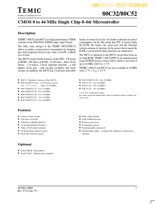
Figure 2. Pin Configuration
80C32/80C52
P1.4 P1.3 P1.2 P1.1/T2EX P1.0/T2 NC VCC P0.0/A0 P0.1/A1 P0.2/A2 P0.3/A3
P1.5 P1.6 P1.7 RST RxD/P3.0
TEMIC’s 80C52 and 80C32 are also available at 16 MHz with 2.7 V < VCC < 5.5 V.
D 80C32 : Romless version of the 80C52 D 80C32/80C52-L16 : Low power version
LCC
80C32/80C52
P04 /A4 P05 /A5 P06 /A6 P07 /A7 EA NC ALE PSEN P27 /A15 P26 /A14 P25 /A13
WR/P36 RD/P37 XTAL2 XTAL1
V SS NC P20 /A8 P21 /A9 P22/A10 P23 /A11 P24/A12
Port 2
Port 2 is an 8 bit bi-directional I/O port with internal pullups. Port 2 pins that have 1’s written to them are pulled high by the internal pullups, and in that state can be used as inputs. As inputs, Port 2 pins that are externally being pulled low will source current (ILL, on the data sheet) because of the internal pullups. Port 2 emits the high-order address byte during fetches from external Program Memory and during accesses to external Data
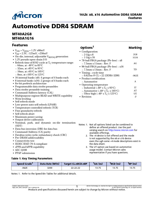
Micron 16Gb x8, x16 汽车级 DDR4 SDRAM 数据手册说明书
Automotive DDR4 SDRAM MT40A2G8MT40A1G16FeaturesNotes:1.Not all options listed can be combined to define an offered product. Use the part catalog search on for available offerings.2.The ×4 device is not offered and the mode is not supported by the x8 or x16 device even tho ugh some ×4 mode descriptions exist in the data sheet.3.The UT option use based on automotive usage model. Contact Micron sales representative if you have questions.Notes:1.Refer to the Speed Bin Tables for additional details.•V DD = V DDQ = 1.2V ±60mV •V PP = 2.5V, –125mV, +250mV •On-die, internal, adjustable V REFDQ generation •1.2V pseudo open-drain I/O •Refresh time of 8192-cycle at T C temperature range:–64ms, at –40°C to 85°C–32ms, at >85°C to 95°C–16ms, at >95°C to 105°C–8ms, at >105°C to 125°C•16 internal banks (x8): 4 groups of 4 banks each•8 internal banks (x16): 2 groups of 4 banks each•8n -bit prefetch architecture•Programmable data strobe preambles•Data strobe preamble training•Command/Address latency (CAL)•Multipurpose register READ and WRITE capability•Write leveling•Self refresh mode•Low-power auto self refresh (LPASR)•Temperature controlled refresh (TCR)•Fine granularity refresh•Self refresh abort•Maximum power saving•Output driver calibration•Nominal, park, and dynamic on-die termination(ODT)•Data bus inversion (DBI) for data bus•Command/Address (CA) parity•Databus write cyclic redundancy check (CRC)•Per-DRAM addressability•Connectivity test•JEDEC JESD-79-4 compliant•sPPR and hPPR capability•AEC-Q100•PPAP submission Options 1Marking •Configuration –2 Gig x 82G8–1 Gig x 161G16•78-ball FBGA package (Pb-free) – x8–7.5mm x 11mm – Rev. F AG •96-ball FBGA package (Pb-free) – x16–7.5mm x 13mm – Rev. F TD •Timing – cycle time –0.625ns @ CL = 22 (DDR4-3200)-062E •Product certification –Automotive A •Operating temperature –Industrial (–40° ≤ T C ≤ 95°C)IT –Automotive (–40° ≤ T C ≤ 105°C)AT –Ultra-high (–40° ≤ T C ≤ 125°C)UT •Revision :F Table 1: Key Timing Parameters Speed Grade 1Data Rate (MT/s)Target CL-n RCD-n RP t AA (ns)t RCD (ns)t RP (ns)-062E 320022-22-2213.7513.7513.75Table 2: AddressingParameter2048 Meg x 81024 Meg x 16 Number of bank groups42Bank group address BG[1:0]BG0Bank count per group44Bank address in bank group BA[1:0]BA[1:0]Row addressing 128K (A[16:0])128K (A[16:0])Column addressing 1K (A[9:0]) 1K (A[9:0])Page size11KB2KBNotes:1.Page size is per bank, calculated as follows:Page size = 2COLBITS× ORG/8, where COLBIT = the number of column address bits and ORG = the number of DQ bits. Figure 1: Order Part Number ExampleExample Part Number: MT40A1G16KH-062E AAT:EContentsImportant Notes and Warnings . . . . . . . . . . . . . . . . . . . . . . . . . . . . . . . . . . . . . . . . . . . . . . . . . . . . . . . . . . . . . . . . . . . . . . . . . 18 General Notes and Description . . . . . . . . . . . . . . . . . . . . . . . . . . . . . . . . . . . . . . . . . . . . . . . . . . . . . . . . . . . . . . . . . . . . . . . . . . 19 Description . . . . . . . . . . . . . . . . . . . . . . . . . . . . . . . . . . . . . . . . . . . . . . . . . . . . . . . . . . . . . . . . . . . . . . . . . . . . . . . . . . . . . . . . . 19 Industrial Temperature . . . . . . . . . . . . . . . . . . . . . . . . . . . . . . . . . . . . . . . . . . . . . . . . . . . . . . . . . . . . . . . . . . . . . . . . . . . . . . 19 Automotive Temperature . . . . . . . . . . . . . . . . . . . . . . . . . . . . . . . . . . . . . . . . . . . . . . . . . . . . . . . . . . . . . . . . . . . . . . . . . . . . 19 Ultra-high Temperature . . . . . . . . . . . . . . . . . . . . . . . . . . . . . . . . . . . . . . . . . . . . . . . . . . . . . . . . . . . . . . . . . . . . . . . . . . . . . . 19 General Notes . . . . . . . . . . . . . . . . . . . . . . . . . . . . . . . . . . . . . . . . . . . . . . . . . . . . . . . . . . . . . . . . . . . . . . . . . . . . . . . . . . . . . . . 19 Definitions of the Device-Pin Signal Level . . . . . . . . . . . . . . . . . . . . . . . . . . . . . . . . . . . . . . . . . . . . . . . . . . . . . . . . . . . . . . 20 Definitions of the Bus Signal Level . . . . . . . . . . . . . . . . . . . . . . . . . . . . . . . . . . . . . . . . . . . . . . . . . . . . . . . . . . . . . . . . . . . . 20 Functional Block Diagrams . . . . . . . . . . . . . . . . . . . . . . . . . . . . . . . . . . . . . . . . . . . . . . . . . . . . . . . . . . . . . . . . . . . . . . . . . . . . . 21 Ball Assignments . . . . . . . . . . . . . . . . . . . . . . . . . . . . . . . . . . . . . . . . . . . . . . . . . . . . . . . . . . . . . . . . . . . . . . . . . . . . . . . . . . . . . . 22 Ball Descriptions . . . . . . . . . . . . . . . . . . . . . . . . . . . . . . . . . . . . . . . . . . . . . . . . . . . . . . . . . . . . . . . . . . . . . . . . . . . . . . . . . . . . . . 24 Package Dimensions . . . . . . . . . . . . . . . . . . . . . . . . . . . . . . . . . . . . . . . . . . . . . . . . . . . . . . . . . . . . . . . . . . . . . . . . . . . . . . . . . . . 27 State Diagram . . . . . . . . . . . . . . . . . . . . . . . . . . . . . . . . . . . . . . . . . . . . . . . . . . . . . . . . . . . . . . . . . . . . . . . . . . . . . . . . . . . . . . . . . 29 Functional Description . . . . . . . . . . . . . . . . . . . . . . . . . . . . . . . . . . . . . . . . . . . . . . . . . . . . . . . . . . . . . . . . . . . . . . . . . . . . . . . . . 31 RESET and Initialization Procedure . . . . . . . . . . . . . . . . . . . . . . . . . . . . . . . . . . . . . . . . . . . . . . . . . . . . . . . . . . . . . . . . . . . . . . 32 Power-Up and Initialization Sequence . . . . . . . . . . . . . . . . . . . . . . . . . . . . . . . . . . . . . . . . . . . . . . . . . . . . . . . . . . . . . . . . . 32 RESET Initialization with Stable Power Sequence . . . . . . . . . . . . . . . . . . . . . . . . . . . . . . . . . . . . . . . . . . . . . . . . . . . . . . . 35 Uncontrolled Power-Down Sequence . . . . . . . . . . . . . . . . . . . . . . . . . . . . . . . . . . . . . . . . . . . . . . . . . . . . . . . . . . . . . . . . . 36 Programming Mode Registers . . . . . . . . . . . . . . . . . . . . . . . . . . . . . . . . . . . . . . . . . . . . . . . . . . . . . . . . . . . . . . . . . . . . . . . . . . . 36 Mode Register 0 . . . . . . . . . . . . . . . . . . . . . . . . . . . . . . . . . . . . . . . . . . . . . . . . . . . . . . . . . . . . . . . . . . . . . . . . . . . . . . . . . . . . . . . 39 Burst Length, Type, and Order . . . . . . . . . . . . . . . . . . . . . . . . . . . . . . . . . . . . . . . . . . . . . . . . . . . . . . . . . . . . . . . . . . . . . . . . 40 CAS Latency . . . . . . . . . . . . . . . . . . . . . . . . . . . . . . . . . . . . . . . . . . . . . . . . . . . . . . . . . . . . . . . . . . . . . . . . . . . . . . . . . . . . . . . . 41 Test Mode . . . . . . . . . . . . . . . . . . . . . . . . . . . . . . . . . . . . . . . . . . . . . . . . . . . . . . . . . . . . . . . . . . . . . . . . . . . . . . . . . . . . . . . . . . 42 Write Recovery (WR)/READ-to-PRECHARGE . . . . . . . . . . . . . . . . . . . . . . . . . . . . . . . . . . . . . . . . . . . . . . . . . . . . . . . . . . . 42 DLL RESET . . . . . . . . . . . . . . . . . . . . . . . . . . . . . . . . . . . . . . . . . . . . . . . . . . . . . . . . . . . . . . . . . . . . . . . . . . . . . . . . . . . . . . . . . 42 Mode Register 1 . . . . . . . . . . . . . . . . . . . . . . . . . . . . . . . . . . . . . . . . . . . . . . . . . . . . . . . . . . . . . . . . . . . . . . . . . . . . . . . . . . . . . . . 43 DLL Enable/DLL Disable . . . . . . . . . . . . . . . . . . . . . . . . . . . . . . . . . . . . . . . . . . . . . . . . . . . . . . . . . . . . . . . . . . . . . . . . . . . . . 44 Output Driver Impedance Control . . . . . . . . . . . . . . . . . . . . . . . . . . . . . . . . . . . . . . . . . . . . . . . . . . . . . . . . . . . . . . . . . . . . 45 ODT R TT(NOM) Values . . . . . . . . . . . . . . . . . . . . . . . . . . . . . . . . . . . . . . . . . . . . . . . . . . . . . . . . . . . . . . . . . . . . . . . . . . . . . . . . 45 Additive Latency . . . . . . . . . . . . . . . . . . . . . . . . . . . . . . . . . . . . . . . . . . . . . . . . . . . . . . . . . . . . . . . . . . . . . . . . . . . . . . . . . . . . 45 Rx CTLE Control . . . . . . . . . . . . . . . . . . . . . . . . . . . . . . . . . . . . . . . . . . . . . . . . . . . . . . . . . . . . . . . . . . . . . . . . . . . . . . . . . . . . . 45 Write Leveling . . . . . . . . . . . . . . . . . . . . . . . . . . . . . . . . . . . . . . . . . . . . . . . . . . . . . . . . . . . . . . . . . . . . . . . . . . . . . . . . . . . . . . . 45 Output Disable . . . . . . . . . . . . . . . . . . . . . . . . . . . . . . . . . . . . . . . . . . . . . . . . . . . . . . . . . . . . . . . . . . . . . . . . . . . . . . . . . . . . . . 45 Termination Data Strobe . . . . . . . . . . . . . . . . . . . . . . . . . . . . . . . . . . . . . . . . . . . . . . . . . . . . . . . . . . . . . . . . . . . . . . . . . . . . . 46 Mode Register 2 . . . . . . . . . . . . . . . . . . . . . . . . . . . . . . . . . . . . . . . . . . . . . . . . . . . . . . . . . . . . . . . . . . . . . . . . . . . . . . . . . . . . . . . 47 CAS WRITE Latency . . . . . . . . . . . . . . . . . . . . . . . . . . . . . . . . . . . . . . . . . . . . . . . . . . . . . . . . . . . . . . . . . . . . . . . . . . . . . . . . . 48 Low-Power Auto Self Refresh . . . . . . . . . . . . . . . . . . . . . . . . . . . . . . . . . . . . . . . . . . . . . . . . . . . . . . . . . . . . . . . . . . . . . . . . . 48 Dynamic ODT . . . . . . . . . . . . . . . . . . . . . . . . . . . . . . . . . . . . . . . . . . . . . . . . . . . . . . . . . . . . . . . . . . . . . . . . . . . . . . . . . . . . . . . 49 Write Cyclic Redundancy Check Data Bus . . . . . . . . . . . . . . . . . . . . . . . . . . . . . . . . . . . . . . . . . . . . . . . . . . . . . . . . . . . . . . 49 Mode Register 3 . . . . . . . . . . . . . . . . . . . . . . . . . . . . . . . . . . . . . . . . . . . . . . . . . . . . . . . . . . . . . . . . . . . . . . . . . . . . . . . . . . . . . . . 50 Multipurpose Register . . . . . . . . . . . . . . . . . . . . . . . . . . . . . . . . . . . . . . . . . . . . . . . . . . . . . . . . . . . . . . . . . . . . . . . . . . . . . . . 51 WRITE Command Latency When CRC/DM is Enabled . . . . . . . . . . . . . . . . . . . . . . . . . . . . . . . . . . . . . . . . . . . . . . . . . . 51 Fine Granularity Refresh Mode . . . . . . . . . . . . . . . . . . . . . . . . . . . . . . . . . . . . . . . . . . . . . . . . . . . . . . . . . . . . . . . . . . . . . . . 52 Temperature Sensor Status . . . . . . . . . . . . . . . . . . . . . . . . . . . . . . . . . . . . . . . . . . . . . . . . . . . . . . . . . . . . . . . . . . . . . . . . . . . 52 Per-DRAM Addressability . . . . . . . . . . . . . . . . . . . . . . . . . . . . . . . . . . . . . . . . . . . . . . . . . . . . . . . . . . . . . . . . . . . . . . . . . . . . 52 Gear-Down Mode . . . . . . . . . . . . . . . . . . . . . . . . . . . . . . . . . . . . . . . . . . . . . . . . . . . . . . . . . . . . . . . . . . . . . . . . . . . . . . . . . . . 52 Mode Register 4 . . . . . . . . . . . . . . . . . . . . . . . . . . . . . . . . . . . . . . . . . . . . . . . . . . . . . . . . . . . . . . . . . . . . . . . . . . . . . . . . . . . . . . . 53 Hard Post Package Repair Mode . . . . . . . . . . . . . . . . . . . . . . . . . . . . . . . . . . . . . . . . . . . . . . . . . . . . . . . . . . . . . . . . . . . . . . 54 Soft Post Package Repair Mode . . . . . . . . . . . . . . . . . . . . . . . . . . . . . . . . . . . . . . . . . . . . . . . . . . . . . . . . . . . . . . . . . . . . . . . 54 WRITE Preamble . . . . . . . . . . . . . . . . . . . . . . . . . . . . . . . . . . . . . . . . . . . . . . . . . . . . . . . . . . . . . . . . . . . . . . . . . . . . . . . . . . . . 55READ Preamble . . . . . . . . . . . . . . . . . . . . . . . . . . . . . . . . . . . . . . . . . . . . . . . . . . . . . . . . . . . . . . . . . . . . . . . . . . . . . . . . . . . . . 55 READ Preamble Training . . . . . . . . . . . . . . . . . . . . . . . . . . . . . . . . . . . . . . . . . . . . . . . . . . . . . . . . . . . . . . . . . . . . . . . . . . . . . 55 Temperature-Controlled Refresh . . . . . . . . . . . . . . . . . . . . . . . . . . . . . . . . . . . . . . . . . . . . . . . . . . . . . . . . . . . . . . . . . . . . . . 55 Command Address Latency . . . . . . . . . . . . . . . . . . . . . . . . . . . . . . . . . . . . . . . . . . . . . . . . . . . . . . . . . . . . . . . . . . . . . . . . . . 55 Internal V REF Monitor . . . . . . . . . . . . . . . . . . . . . . . . . . . . . . . . . . . . . . . . . . . . . . . . . . . . . . . . . . . . . . . . . . . . . . . . . . . . . . . . 55 Maximum Power Savings Mode . . . . . . . . . . . . . . . . . . . . . . . . . . . . . . . . . . . . . . . . . . . . . . . . . . . . . . . . . . . . . . . . . . . . . . . 55 Mode Register 5 . . . . . . . . . . . . . . . . . . . . . . . . . . . . . . . . . . . . . . . . . . . . . . . . . . . . . . . . . . . . . . . . . . . . . . . . . . . . . . . . . . . . . . . 56 Data Bus Inversion . . . . . . . . . . . . . . . . . . . . . . . . . . . . . . . . . . . . . . . . . . . . . . . . . . . . . . . . . . . . . . . . . . . . . . . . . . . . . . . . . . 57 Data Mask . . . . . . . . . . . . . . . . . . . . . . . . . . . . . . . . . . . . . . . . . . . . . . . . . . . . . . . . . . . . . . . . . . . . . . . . . . . . . . . . . . . . . . . . . . 57 CA Parity Persistent Error Mode . . . . . . . . . . . . . . . . . . . . . . . . . . . . . . . . . . . . . . . . . . . . . . . . . . . . . . . . . . . . . . . . . . . . . . . 58 ODT Input Buffer for Power-Down . . . . . . . . . . . . . . . . . . . . . . . . . . . . . . . . . . . . . . . . . . . . . . . . . . . . . . . . . . . . . . . . . . . . 58 CA Parity Error Status . . . . . . . . . . . . . . . . . . . . . . . . . . . . . . . . . . . . . . . . . . . . . . . . . . . . . . . . . . . . . . . . . . . . . . . . . . . . . . . . 58 CRC Error Status . . . . . . . . . . . . . . . . . . . . . . . . . . . . . . . . . . . . . . . . . . . . . . . . . . . . . . . . . . . . . . . . . . . . . . . . . . . . . . . . . . . . 58 CA Parity Latency Mode . . . . . . . . . . . . . . . . . . . . . . . . . . . . . . . . . . . . . . . . . . . . . . . . . . . . . . . . . . . . . . . . . . . . . . . . . . . . . . 58 Mode Register 6 . . . . . . . . . . . . . . . . . . . . . . . . . . . . . . . . . . . . . . . . . . . . . . . . . . . . . . . . . . . . . . . . . . . . . . . . . . . . . . . . . . . . . . . 59 Data Rate Programming . . . . . . . . . . . . . . . . . . . . . . . . . . . . . . . . . . . . . . . . . . . . . . . . . . . . . . . . . . . . . . . . . . . . . . . . . . . . . . 60 V REFDQ Calibration Enable . . . . . . . . . . . . . . . . . . . . . . . . . . . . . . . . . . . . . . . . . . . . . . . . . . . . . . . . . . . . . . . . . . . . . . . . . . . 60 V REFDQ Calibration Range . . . . . . . . . . . . . . . . . . . . . . . . . . . . . . . . . . . . . . . . . . . . . . . . . . . . . . . . . . . . . . . . . . . . . . . . . . . . 60 V REFDQ Calibration Value . . . . . . . . . . . . . . . . . . . . . . . . . . . . . . . . . . . . . . . . . . . . . . . . . . . . . . . . . . . . . . . . . . . . . . . . . . . . . 60 Truth Tables . . . . . . . . . . . . . . . . . . . . . . . . . . . . . . . . . . . . . . . . . . . . . . . . . . . . . . . . . . . . . . . . . . . . . . . . . . . . . . . . . . . . . . . . 61 NOP Command . . . . . . . . . . . . . . . . . . . . . . . . . . . . . . . . . . . . . . . . . . . . . . . . . . . . . . . . . . . . . . . . . . . . . . . . . . . . . . . . . . . . . . . 66 DESELECT Command . . . . . . . . . . . . . . . . . . . . . . . . . . . . . . . . . . . . . . . . . . . . . . . . . . . . . . . . . . . . . . . . . . . . . . . . . . . . . . . . . . 66 DLL-Off Mode . . . . . . . . . . . . . . . . . . . . . . . . . . . . . . . . . . . . . . . . . . . . . . . . . . . . . . . . . . . . . . . . . . . . . . . . . . . . . . . . . . . . . . . . . 66 DLL-On/Off Switching Procedures . . . . . . . . . . . . . . . . . . . . . . . . . . . . . . . . . . . . . . . . . . . . . . . . . . . . . . . . . . . . . . . . . . . . . . 68 DLL Switch Sequence from DLL-On to DLL-Off . . . . . . . . . . . . . . . . . . . . . . . . . . . . . . . . . . . . . . . . . . . . . . . . . . . . . . . . . 68 DLL-Off to DLL-On Procedure . . . . . . . . . . . . . . . . . . . . . . . . . . . . . . . . . . . . . . . . . . . . . . . . . . . . . . . . . . . . . . . . . . . . . . . . 70 Input Clock Frequency Change . . . . . . . . . . . . . . . . . . . . . . . . . . . . . . . . . . . . . . . . . . . . . . . . . . . . . . . . . . . . . . . . . . . . . . . . . . 71 Write Leveling . . . . . . . . . . . . . . . . . . . . . . . . . . . . . . . . . . . . . . . . . . . . . . . . . . . . . . . . . . . . . . . . . . . . . . . . . . . . . . . . . . . . . . . . . 71 DRAM Setting for Write Leveling and DRAM TERMINATION Function in that Mode . . . . . . . . . . . . . . . . . . . . . . . 73 Procedure Description . . . . . . . . . . . . . . . . . . . . . . . . . . . . . . . . . . . . . . . . . . . . . . . . . . . . . . . . . . . . . . . . . . . . . . . . . . . . . . . 73 Write Leveling Mode Exit . . . . . . . . . . . . . . . . . . . . . . . . . . . . . . . . . . . . . . . . . . . . . . . . . . . . . . . . . . . . . . . . . . . . . . . . . . . . . 75 Command Address Latency . . . . . . . . . . . . . . . . . . . . . . . . . . . . . . . . . . . . . . . . . . . . . . . . . . . . . . . . . . . . . . . . . . . . . . . . . . . . . 76 Low-Power Auto Self Refresh Mode . . . . . . . . . . . . . . . . . . . . . . . . . . . . . . . . . . . . . . . . . . . . . . . . . . . . . . . . . . . . . . . . . . . . . . 80 Manual Self Refresh Mode . . . . . . . . . . . . . . . . . . . . . . . . . . . . . . . . . . . . . . . . . . . . . . . . . . . . . . . . . . . . . . . . . . . . . . . . . . . . 80 Multipurpose Register . . . . . . . . . . . . . . . . . . . . . . . . . . . . . . . . . . . . . . . . . . . . . . . . . . . . . . . . . . . . . . . . . . . . . . . . . . . . . . . . . . 82 MPR Reads . . . . . . . . . . . . . . . . . . . . . . . . . . . . . . . . . . . . . . . . . . . . . . . . . . . . . . . . . . . . . . . . . . . . . . . . . . . . . . . . . . . . . . . . . 83 MPR Readout Format . . . . . . . . . . . . . . . . . . . . . . . . . . . . . . . . . . . . . . . . . . . . . . . . . . . . . . . . . . . . . . . . . . . . . . . . . . . . . . . . 85 MPR Readout Serial Format . . . . . . . . . . . . . . . . . . . . . . . . . . . . . . . . . . . . . . . . . . . . . . . . . . . . . . . . . . . . . . . . . . . . . . . . . . 85 MPR Readout Parallel Format . . . . . . . . . . . . . . . . . . . . . . . . . . . . . . . . . . . . . . . . . . . . . . . . . . . . . . . . . . . . . . . . . . . . . . . . . 86 MPR Readout Staggered Format . . . . . . . . . . . . . . . . . . . . . . . . . . . . . . . . . . . . . . . . . . . . . . . . . . . . . . . . . . . . . . . . . . . . . . 87 MPR READ Waveforms . . . . . . . . . . . . . . . . . . . . . . . . . . . . . . . . . . . . . . . . . . . . . . . . . . . . . . . . . . . . . . . . . . . . . . . . . . . . . . . 88 MPR Writes . . . . . . . . . . . . . . . . . . . . . . . . . . . . . . . . . . . . . . . . . . . . . . . . . . . . . . . . . . . . . . . . . . . . . . . . . . . . . . . . . . . . . . . . . 90 MPR WRITE Waveforms . . . . . . . . . . . . . . . . . . . . . . . . . . . . . . . . . . . . . . . . . . . . . . . . . . . . . . . . . . . . . . . . . . . . . . . . . . . . . . 90 MPR REFRESH Waveforms . . . . . . . . . . . . . . . . . . . . . . . . . . . . . . . . . . . . . . . . . . . . . . . . . . . . . . . . . . . . . . . . . . . . . . . . . . . 92 Gear-Down Mode . . . . . . . . . . . . . . . . . . . . . . . . . . . . . . . . . . . . . . . . . . . . . . . . . . . . . . . . . . . . . . . . . . . . . . . . . . . . . . . . . . . . . . 94 Maximum Power-Saving Mode . . . . . . . . . . . . . . . . . . . . . . . . . . . . . . . . . . . . . . . . . . . . . . . . . . . . . . . . . . . . . . . . . . . . . . . . . . 97 Maximum Power-Saving Mode Entry . . . . . . . . . . . . . . . . . . . . . . . . . . . . . . . . . . . . . . . . . . . . . . . . . . . . . . . . . . . . . . . . . . 97 Maximum Power-Saving Mode Entry in PDA . . . . . . . . . . . . . . . . . . . . . . . . . . . . . . . . . . . . . . . . . . . . . . . . . . . . . . . . . . . 98 CKE Transition During Maximum Power-Saving Mode . . . . . . . . . . . . . . . . . . . . . . . . . . . . . . . . . . . . . . . . . . . . . . . . . . 98 Maximum Power-Saving Mode Exit . . . . . . . . . . . . . . . . . . . . . . . . . . . . . . . . . . . . . . . . . . . . . . . . . . . . . . . . . . . . . . . . . . . 98 Command/Address Parity . . . . . . . . . . . . . . . . . . . . . . . . . . . . . . . . . . . . . . . . . . . . . . . . . . . . . . . . . . . . . . . . . . . . . . . . . . . . .100 Per-DRAM Addressability . . . . . . . . . . . . . . . . . . . . . . . . . . . . . . . . . . . . . . . . . . . . . . . . . . . . . . . . . . . . . . . . . . . . . . . . . . . . . .107V REFDQ Range and Levels . . . . . . . . . . . . . . . . . . . . . . . . . . . . . . . . . . . . . . . . . . . . . . . . . . . . . . . . . . . . . . . . . . . . . . . . . . . .111V REFDQ Step Size . . . . . . . . . . . . . . . . . . . . . . . . . . . . . . . . . . . . . . . . . . . . . . . . . . . . . . . . . . . . . . . . . . . . . . . . . . . . . . . . . . .111V REFDQ Increment and Decrement Timing . . . . . . . . . . . . . . . . . . . . . . . . . . . . . . . . . . . . . . . . . . . . . . . . . . . . . . . . . . . .112V REFDQ Target Settings . . . . . . . . . . . . . . . . . . . . . . . . . . . . . . . . . . . . . . . . . . . . . . . . . . . . . . . . . . . . . . . . . . . . . . . . . . . . . .116Connectivity Test Mode . . . . . . . . . . . . . . . . . . . . . . . . . . . . . . . . . . . . . . . . . . . . . . . . . . . . . . . . . . . . . . . . . . . . . . . . . . . . . . .118Pin Mapping . . . . . . . . . . . . . . . . . . . . . . . . . . . . . . . . . . . . . . . . . . . . . . . . . . . . . . . . . . . . . . . . . . . . . . . . . . . . . . . . . . . . . . .118Minimum Terms Definition for Logic Equations . . . . . . . . . . . . . . . . . . . . . . . . . . . . . . . . . . . . . . . . . . . . . . . . . . . . . . .119Logic Equations for a x4 Device . . . . . . . . . . . . . . . . . . . . . . . . . . . . . . . . . . . . . . . . . . . . . . . . . . . . . . . . . . . . . . . . . . . . . .119Logic Equations for a x8 Device . . . . . . . . . . . . . . . . . . . . . . . . . . . . . . . . . . . . . . . . . . . . . . . . . . . . . . . . . . . . . . . . . . . . . .120Logic Equations for a x16 Device . . . . . . . . . . . . . . . . . . . . . . . . . . . . . . . . . . . . . . . . . . . . . . . . . . . . . . . . . . . . . . . . . . . . .120CT Input Timing Requirements . . . . . . . . . . . . . . . . . . . . . . . . . . . . . . . . . . . . . . . . . . . . . . . . . . . . . . . . . . . . . . . . . . . . . .120Excessive Row Activation . . . . . . . . . . . . . . . . . . . . . . . . . . . . . . . . . . . . . . . . . . . . . . . . . . . . . . . . . . . . . . . . . . . . . . . . . . . . . .122Post Package Repair . . . . . . . . . . . . . . . . . . . . . . . . . . . . . . . . . . . . . . . . . . . . . . . . . . . . . . . . . . . . . . . . . . . . . . . . . . . . . . . . . . .123Post Package Repair . . . . . . . . . . . . . . . . . . . . . . . . . . . . . . . . . . . . . . . . . . . . . . . . . . . . . . . . . . . . . . . . . . . . . . . . . . . . . . . .123Hard Post Package Repair . . . . . . . . . . . . . . . . . . . . . . . . . . . . . . . . . . . . . . . . . . . . . . . . . . . . . . . . . . . . . . . . . . . . . . . . . . . . . .123hPPR Row Repair - Entry . . . . . . . . . . . . . . . . . . . . . . . . . . . . . . . . . . . . . . . . . . . . . . . . . . . . . . . . . . . . . . . . . . . . . . . . . . . .124hPPR Row Repair – WRA Initiated (REF Commands Allowed) . . . . . . . . . . . . . . . . . . . . . . . . . . . . . . . . . . . . . . . . . . .124hPPR Row Repair – WR Initiated (REF Commands NOT Allowed) . . . . . . . . . . . . . . . . . . . . . . . . . . . . . . . . . . . . . . . .126sPPR Row Repair . . . . . . . . . . . . . . . . . . . . . . . . . . . . . . . . . . . . . . . . . . . . . . . . . . . . . . . . . . . . . . . . . . . . . . . . . . . . . . . . . . . . . .127hPPR/sPPR/MBIST-PPR Support Identifier . . . . . . . . . . . . . . . . . . . . . . . . . . . . . . . . . . . . . . . . . . . . . . . . . . . . . . . . . . . . . .130ACTIVATE Command . . . . . . . . . . . . . . . . . . . . . . . . . . . . . . . . . . . . . . . . . . . . . . . . . . . . . . . . . . . . . . . . . . . . . . . . . . . . . . . . .130PRECHARGE Command . . . . . . . . . . . . . . . . . . . . . . . . . . . . . . . . . . . . . . . . . . . . . . . . . . . . . . . . . . . . . . . . . . . . . . . . . . . . . . .131REFRESH Command . . . . . . . . . . . . . . . . . . . . . . . . . . . . . . . . . . . . . . . . . . . . . . . . . . . . . . . . . . . . . . . . . . . . . . . . . . . . . . . . . .132Temperature-Controlled Refresh Mode . . . . . . . . . . . . . . . . . . . . . . . . . . . . . . . . . . . . . . . . . . . . . . . . . . . . . . . . . . . . . . . . .134Normal Temperature Mode . . . . . . . . . . . . . . . . . . . . . . . . . . . . . . . . . . . . . . . . . . . . . . . . . . . . . . . . . . . . . . . . . . . . . . . . .134Extended Temperature Mode . . . . . . . . . . . . . . . . . . . . . . . . . . . . . . . . . . . . . . . . . . . . . . . . . . . . . . . . . . . . . . . . . . . . . . . .134Fine Granularity Refresh Mode . . . . . . . . . . . . . . . . . . . . . . . . . . . . . . . . . . . . . . . . . . . . . . . . . . . . . . . . . . . . . . . . . . . . . . . . .136Mode Register and Command Truth Table . . . . . . . . . . . . . . . . . . . . . . . . . . . . . . . . . . . . . . . . . . . . . . . . . . . . . . . . . . . .136 t REFI and t RFC Parameters . . . . . . . . . . . . . . . . . . . . . . . . . . . . . . . . . . . . . . . . . . . . . . . . . . . . . . . . . . . . . . . . . . . . . . . . . .136 Changing Refresh Rate . . . . . . . . . . . . . . . . . . . . . . . . . . . . . . . . . . . . . . . . . . . . . . . . . . . . . . . . . . . . . . . . . . . . . . . . . . . . . .139Usage with TCR Mode . . . . . . . . . . . . . . . . . . . . . . . . . . . . . . . . . . . . . . . . . . . . . . . . . . . . . . . . . . . . . . . . . . . . . . . . . . . . . .139Self Refresh Entry and Exit . . . . . . . . . . . . . . . . . . . . . . . . . . . . . . . . . . . . . . . . . . . . . . . . . . . . . . . . . . . . . . . . . . . . . . . . . . .139SELF REFRESH Operation . . . . . . . . . . . . . . . . . . . . . . . . . . . . . . . . . . . . . . . . . . . . . . . . . . . . . . . . . . . . . . . . . . . . . . . . . . . . .141Self Refresh Abort . . . . . . . . . . . . . . . . . . . . . . . . . . . . . . . . . . . . . . . . . . . . . . . . . . . . . . . . . . . . . . . . . . . . . . . . . . . . . . . . . .143Self Refresh Exit with NOP Command . . . . . . . . . . . . . . . . . . . . . . . . . . . . . . . . . . . . . . . . . . . . . . . . . . . . . . . . . . . . . . . .144Power-Down Mode . . . . . . . . . . . . . . . . . . . . . . . . . . . . . . . . . . . . . . . . . . . . . . . . . . . . . . . . . . . . . . . . . . . . . . . . . . . . . . . . . . .146Power-Down Clarifications – Case 1 . . . . . . . . . . . . . . . . . . . . . . . . . . . . . . . . . . . . . . . . . . . . . . . . . . . . . . . . . . . . . . . . . .151Power-Down Entry, Exit Timing with CAL . . . . . . . . . . . . . . . . . . . . . . . . . . . . . . . . . . . . . . . . . . . . . . . . . . . . . . . . . . . . .152ODT Input Buffer Disable Mode for Power-Down . . . . . . . . . . . . . . . . . . . . . . . . . . . . . . . . . . . . . . . . . . . . . . . . . . . . . . . .154CRC Write Data Feature . . . . . . . . . . . . . . . . . . . . . . . . . . . . . . . . . . . . . . . . . . . . . . . . . . . . . . . . . . . . . . . . . . . . . . . . . . . . . . .156CRC Write Data . . . . . . . . . . . . . . . . . . . . . . . . . . . . . . . . . . . . . . . . . . . . . . . . . . . . . . . . . . . . . . . . . . . . . . . . . . . . . . . . . . . .156WRITE CRC DATA Operation . . . . . . . . . . . . . . . . . . . . . . . . . . . . . . . . . . . . . . . . . . . . . . . . . . . . . . . . . . . . . . . . . . . . . . . .156DBI_n and CRC Both Enabled . . . . . . . . . . . . . . . . . . . . . . . . . . . . . . . . . . . . . . . . . . . . . . . . . . . . . . . . . . . . . . . . . . . . . . .157DM_n and CRC Both Enabled . . . . . . . . . . . . . . . . . . . . . . . . . . . . . . . . . . . . . . . . . . . . . . . . . . . . . . . . . . . . . . . . . . . . . . . .157DM_n and DBI_n Conflict During Writes with CRC Enabled . . . . . . . . . . . . . . . . . . . . . . . . . . . . . . . . . . . . . . . . . . . .157CRC and Write Preamble Restrictions . . . . . . . . . . . . . . . . . . . . . . . . . . . . . . . . . . . . . . . . . . . . . . . . . . . . . . . . . . . . . . . .157CRC Simultaneous Operation Restrictions . . . . . . . . . . . . . . . . . . . . . . . . . . . . . . . . . . . . . . . . . . . . . . . . . . . . . . . . . . . .157CRC Polynomial . . . . . . . . . . . . . . . . . . . . . . . . . . . . . . . . . . . . . . . . . . . . . . . . . . . . . . . . . . . . . . . . . . . . . . . . . . . . . . . . . . . .157CRC Combinatorial Logic Equations . . . . . . . . . . . . . . . . . . . . . . . . . . . . . . . . . . . . . . . . . . . . . . . . . . . . . . . . . . . . . . . . . .158Burst Ordering for BL8 . . . . . . . . . . . . . . . . . . . . . . . . . . . . . . . . . . . . . . . . . . . . . . . . . . . . . . . . . . . . . . . . . . . . . . . . . . . . . .159CRC Data Bit Mapping . . . . . . . . . . . . . . . . . . . . . . . . . . . . . . . . . . . . . . . . . . . . . . . . . . . . . . . . . . . . . . . . . . . . . . . . . . . . . .159CRC Enabled With BC4 . . . . . . . . . . . . . . . . . . . . . . . . . . . . . . . . . . . . . . . . . . . . . . . . . . . . . . . . . . . . . . . . . . . . . . . . . . . . . .160。
MEMORY存储芯片M25P16-VMC6TG中文规格书
Micron M25P16 Serial Flash Embedded Memory16Mb, 3V Features•SPI bus compatible serial interface •16Mb Flash memory•75 MHz clock frequency (maximum)•2.7V to 3.6V single supply voltage•Page program (up to 256 bytes) in 0.64ms (TYP)•Erase capability–Sector erase: 512Kb in 0.6 s (TYP)–Bulk erase: 16Mb in 13 s (TYP)•Write protection–Hardware write protection: protected area size defined by non-volatile bits BP0, BP1, BP2•Deep power down: 1µA (TYP)•Electronic signature–JEDEC standard 2-byte signature (2015h)–Unique ID code (UID) and 16 bytes of read-only data, available upon customer request–RES command, one-byte signature (14h) for backward compatibility•More than 100,000 write cycles per sector •More than 20 years data retention •Automotive grade parts available •Packages (RoHS compliant)–SO8N (MN) 150 mils –SO8W (MW) 208 mils –SO16 (MF) 300 mils–VFDFPN8 (MP) MLP8 6mm x 5mm –VFDFPN8 (ME) MLP8 8mm x 6mm –UFDFPN8 (MC) MLP8 4mm x 3mmMicron M25P16 Serial Flash Embedded MemoryImportant Notes and WarningsFunctional DescriptionThe M25P16 is an 16Mb (2Mb x 8) serial Flash memory device with advanced write pro-tection mechanisms accessed by a high speed SPI-compatible bus. The device supports high-performance commands for clock frequency up to 75MHz.The memory can be programmed 1 to 256 bytes at a time using the PAGE PROGRAM command. It is organized as 32 sectors, each containing 256 pages. Each page is 256bytes wide. Memory can be viewed either as 8,192 pages or as 2,097,152 bytes. The en-tire memory can be erased using the BULK ERASE command, or it can be erased one sector at a time using the SECTOR ERASE command.This datasheet details the functionality of the M25P16 device based on 110nm process.Figure 1: Logic DiagramS#V CCHOLD#V SSDQ1C DQ0W#Table 1: Signal NamesMicron M25P16 Serial Flash Embedded MemoryFunctional DescriptionFigure 5: Bus Master and Memory Devices on the SPI BusSS2.Resistors (R) ensure that the memory device is not selected if the bus master leaves theS# line High-Z.3.The bus master may enter a state where all I/O are High-Z at the same time; for exam-ple, when the bus master is reset. Therefore, C must be connected to an external pull-down resistor so that when all I/O are High-Z, S# is pulled HIGH while C is pulled LOW.This ensures that S# and C do not go HIGH at the same time and that the t SHCH require-ment is met.4.The typical value of R is 100kΩ, assuming that the time constant R × C p (C p = parasiticcapacitance of the bus line) is shorter than the time during which the bus master leavesthe SPI bus High-Z.5.Example: Given that C p = 50pF (R × C p= 5μs), the application must ensure that the busmaster never leaves the SPI bus High-Z for a time period shorter than 5μs.质量等级领域:宇航级IC、特军级IC、超军级IC、普军级IC、禁运IC、工业级IC,军级二三极管,功率管等;应用领域:航空航天、船舶、汽车电子、军用计算机、铁路、医疗电子、通信网络、电力工业以及大型工业设备祝您:工作顺利,生活愉快!以深圳市美光存储技术有限公司提供的参数为例,以下为M25P16-VMC6TG的详细参数,仅供参考。
莫加 MPC-2121 系列 12英寸无风扇车辆面板计算机商品介绍说明书

MPC-2121Series12-inch industrial fanless panel computers with EN50155compliance for the railway marketFeatures and Benefits•12-inch panel computer•Intel Atom®processor E38451.91GHz•1000-nit sunlight-readable LCD•-40to70°C wide-temperature design,no fan or heater•EN50155:2017CompliantCertificationsIntroductionThe MPC-212112-inch panel computers with E3800Series Intel Atom®processor deliver a reliable,durable,and versatile platform for use in industrial environments.All interfaces come with IP66-rated M12connectors to provide anti-vibration and waterproof connections.With two software-selectable RS-232/422/485serial ports and two Ethernet ports,the MPC-2121panel computers support a wide variety of serial interfaces as well as high-speed IT communications,all with native network redundancy.The MPC-2121Series panel computers are designed with a wide,-40to70°C temperature range,and come with a fanless,streamlined enclosure designed for highly efficient heat dissipation,making this one of the most reliable industrial platforms available for vibration prone,harsh,hot, outdoor environments.The MPC-2121also features a1000-nit LCD panel offering a sunlight readable,projected-capacitive,multi-touch screen, providing an excellent user experience.AppearanceSpecificationsComputerCPU Intel Atom®Processor E3845(2M Cache,1.91GHz)Graphics Controller Intel®HD GraphicsSystem Memory Pre-installed4(8GB Max.)GB DDR3LSystem Memory Slot SODIMM DDR3/DDR3L slot x1Pre-installed OS MPC-2121-E4-LB-CT-T-W7E/MPC-2101-E4-CT-T-W7E:Windows Embedded Standard7(WS7P)64-bit pre-installedMPC-2121-E4-LB-CT-T-LX/MPC-2121-E4-CT-T-LX:Linux9pre-installedSupported OS Windows10Pro64-bitWindows10Embedded IoT Ent2019LTSC64-bitWindows10Embedded IoT Ent2016LTSBWindows7Pro for Embedded SystemsWindows Embedded Standard7(WS7P)64-bitLinux Debian9Expansion Slots Mini PCIeStorage Slot CFast slot x1SD slots x1,SD3.0(SDHC/SDXC)socketStorage Pre-installed MPC-2121-E4-LB-CT-T-W7E/MPC-2121-E4-CT-T-W7E:32GB CFast CardMPC-2121-E4-LB-CT-T-LX/MPC-2121-E4-CT-T-LX:32GB CFast CardComputer InterfaceEthernet Ports Auto-sensing10/100Mbps ports(M12D-coded4P)x2Serial Ports RS-232/422/485ports x1(M12A-code12P)USB2.0USB2.0hosts x1(M12A-coded5P)Digital Input DIs x4(M12A-code)Digital Output DOs x2(M12A-code)LED IndicatorsSystem Power x1DisplayActive Display Area245.76(H)x184.32(V)mmAspect Ratio4:3Contrast Ratio1000:1Light Intensity(Brightness)500/1000cd/m2Max.No.of Colors16.2M(8-bit/color)Panel Size12-inch viewable imagePixel Pitch(RGB)0.240(H)x0.240(V)mmPixels1024x768Response Time5ms(gray to gray)Viewing Angles176°/176°Touch FunctionTouch Type Capacitive Touch(PCAP)Touch Support Points4pointsGlove Support YesSerial InterfaceBaudrate50bps to115.2kbpsData Bits5,6,7,8Flow Control RTS/CTS,XON/XOFFParity None,Even,Odd,Space,MarkStop Bits1,1.5,2Serial SignalsRS-232TxD,RxD,RTS,CTS,DTR,DSR,DCD,GND RS-422Tx+,Tx-,Rx+,Rx-,GNDRS-485-2w Data+,Data-,GNDRS-485-4w Tx+,Tx-,Rx+,Rx-,GNDPower ParametersInput Voltage24to110VDCPhysical CharacteristicsHousing MetalIP Rating IP66Dimensions297x238x59mm(11.69x9.37x2.32in) Weight2850g(6.28lb)Environmental LimitsOperating Temperature-40to70°C(-40to158°F)Storage Temperature(package included)-40to70°C(-40to158°F)Ambient Relative Humidity5to95%(non-condensing)Standards and CertificationsEMI CISPR32,FCC Part15B Class AEMS IEC61000-4-2ESD:Contact:6kV;Air:8kVIEC61000-4-3RS:80MHz to1GHz:20V/mIEC61000-4-4EFT:Power:2kV;Signal:2kVIEC61000-4-5Surge:Power:2kV;Signal:1kVIEC61000-4-6CS:10VIEC61000-4-8PFMFMechanical Protection Rating IEC60529,IP codeShock EN50155standardVibration EN50155standardEMC EN55032/35Safety IEC60950-1,IEC62368-1,UL62368-1 DeclarationGreen Product RoHS,CRoHS,WEEEWarrantyWarranty Period LCD:1yearSystem:3yearsDetails See /warrantyPackage ContentsDevice1x MPC-2121Series computerInstallation Kit6x screw,for panel-mounting1x M12-Phone jack power cable1x M12-Type A USB cable1x terminal block,2-pin(for remote power input) Documentation1x quick installation guide1x warranty cardDimensionsOrdering Information2.0MPC-2121-E4-LB-CT-T-W7E 12"(4:3)500nitsE3845Quadcore4GBW7E(64-bit)2(M12)1(M12)1(M12)4/2(M12)24to110VDCIP66-40to70°CMPC-2121-E4-CT-T-W7E12"(4:3)1,000nitsE3845Quadcore4GBW7E(64-bit)2(M12)1(M12)1(M12)4/2(M12)24to110VDCIP66-40to70°CMPC-2121-E4-LB-CT-T-LX 12"(4:3)500nitsE3845Quadcore4GB Debian92(M12)1(M12)1(M12)4/2(M12)24to110VDCIP66-40to70°CMPC-2121-E4-CT-T-LX12"(4:3)1,000nitsE3845Quadcore4GB Debian92(M12)1(M12)1(M12)4/2(M12)24to110VDCIP66-40to70°CMPC-2121-E4-LB-CT-T 12"(4:3)500nitsE3845Quadcore4GB–2(M12)1(M12)1(M12)4/2(M12)24to110VDCIP66-40to70°CMPC-2121-E4-CT-T12"(4:3)1,000nitsE3845Quadcore4GB–2(M12)1(M12)1(M12)4/2(M12)24to110VDCIP66-40to70°C©Moxa Inc.All rights reserved.Updated Jun28,2021.This document and any portion thereof may not be reproduced or used in any manner whatsoever without the express written permission of Moxa Inc.Product specifications subject to change without notice.Visit our website for the most up-to-date product information.。
MT8KTF51264HZ-1G6E1
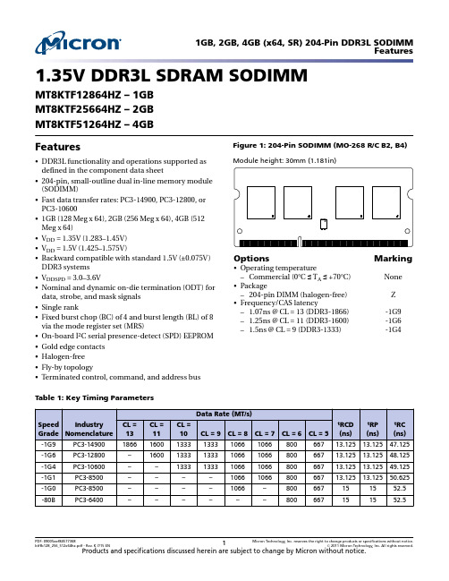
1.35V DDR3L SDRAM SODIMMMT8KTF12864HZ – 1GB MT8KTF25664HZ – 2GB MT8KTF51264HZ – 4GB Features•DDR3L functionality and operations supported as defined in the component data sheet•204-pin, small-outline dual in-line memory module (SODIMM)•Fast data transfer rates: PC3-14900, PC3-12800, or PC3-10600•1GB (128 Meg x 64), 2GB (256 Meg x 64), 4GB (512Meg x 64)•V DD = 1.35V (1.283–1.45V)•V DD = 1.5V (1.425–1.575V)•Backward compatible with standard 1.5V (±0.075V)DDR3 systems •V DDSPD = 3.0–3.6V•Nominal and dynamic on-die termination (ODT) for data, strobe, and mask signals •Single rank•Fixed burst chop (BC) of 4 and burst length (BL) of 8via the mode register set (MRS)•On-board I 2C serial presence-detect (SPD) EEPROM •Gold edge contacts •Halogen-free •Fly-by topology•Terminated control, command, and address bus Figure 1: 204-Pin SODIMM (MO-268 R/C B2, B4)Module height: 30mm (1.181in)OptionsMarking•Operating temperature–Commercial (0°C ≤ T A ≤ +70°C)None •Package–204-pin DIMM (halogen-free)Z •Frequency/CAS latency– 1.07ns @ CL = 13 (DDR3-1866)-1G9– 1.25ns @ CL = 11 (DDR3-1600)-1G6– 1.5ns @ CL = 9 (DDR3-1333)-1G4Table 1: Key Timing ParametersTable 2: AddressingTable 3: Part Numbers and Timing Parameters – 1GB Modules1Table 4: Part Numbers and Timing Parameters – 2GB Modules1Table 5: Part Numbers and Timing Parameters – 4GB Modules1Notes: 1.The data sheet for the base device can be found on Micron’s web site.2.All part numbers end with a two-place code (not shown) that designates component and PCB revisions.Consult factory for current revision codes. Example: MT8KSF51264HZ-1G9P1.Pin AssignmentsTable 6: Pin AssignmentsNotes: 1.Pin 78 is NF for 1GB and 2GB; A15 for 4GB.2.Pin 80 is NF for 1GB; A14 for 2GB and 4GB.Pin DescriptionsThe pin description table below is a comprehensive list of all possible pins for all DDR3modules. All pins listed may not be supported on this module. See Pin Assignments forinformation specific to this module.Table 7: Pin DescriptionsTable 7: Pin Descriptions (Continued)DQ MapsTable 8: Component-to-Module DQ Map, R/C B2 (PCB 1092)Table 9: Component-to-Module DQ Map, R/C B4 (PCB 1348)Functional Block Diagram Figure 2: Functional Block DiagramS0#A[15/14/13:0]RAS#WE#CKE0A[15/14/13:0]: DDR3 SDRAMWE#: DDR3 SDRAMCKE0: DDR3 SDRAMRESET#: DDR3 SDRAMCK0CK0#CK1CK1#V REFCAV SSV DDControl, command,and address terminationV DDSPDV TTV REFDQClock, control, command, and address line terminations:TTV DDNote: 1.The ZQ ball on each DDR3 component is connected to an external 240Ω ±1% resistorthat is tied to ground. It is used for the calibration of the component’s ODT and outputdriver.1GB, 2GB, 4GB (x64, SR) 204-Pin DDR3L SODIMMFunctional Block DiagramGeneral DescriptionDDR3 SDRAM modules are high-speed, CMOS dynamic random access memory mod-ules that use internally configured 8-bank DDR3 SDRAM devices. DDR3 SDRAM mod-ules use DDR architecture to achieve high-speed operation. DDR3 architecture is essen-tially an 8n-prefetch architecture with an interface designed to transfer two data wordsper clock cycle at the I/O pins. A single read or write access for the DDR3 SDRAM mod-ule effectively consists of a single 8n-bit-wide, one-clock-cycle data transfer at the inter-nal DRAM core and eight corresponding n-bit-wide, one-half-clock-cycle data transfersat the I/O pins.DDR3 modules use two sets of differential signals: DQS, DQS# to capture data and CKand CK# to capture commands, addresses, and control signals. Differential clocks anddata strobes ensure exceptional noise immunity for these signals and provide precisecrossing points to capture input signals.Fly-By TopologyDDR3 modules use faster clock speeds than earlier DDR technologies, making signalquality more important than ever. For improved signal quality, the clock, control, com-mand, and address buses have been routed in a fly-by topology, where each clock, con-trol, command, and address pin on each DRAM is connected to a single trace and ter-minated (rather than a tree structure, where the termination is off the module near theconnector). Inherent to fly-by topology, the timing skew between the clock and DQS sig-nals can be easily accounted for by using the write-leveling feature of DDR3.Serial Presence-Detect EEPROM OperationDDR3 SDRAM modules incorporate serial presence-detect. The SPD data is stored in a256-byte EEPROM. The first 128 bytes are programmed by Micron to comply withJEDEC standard JC-45, "Appendix X: Serial Presence Detect (SPD) for DDR3 SDRAMModules." These bytes identify module-specific timing parameters, configuration infor-mation, and physical attributes. The remaining 128 bytes of storage are available for useby the customer. System READ/WRITE operations between the master (system logic)and the slave EEPROM device occur via a standard I2C bus using the DIMM’s SCL(clock) SDA (data), and SA (address) pins. Write protect (WP) is connected to V SS, per-manently disabling hardware write protection. For further information refer to Microntechnical note TN-04-42, "Memory Module Serial Presence-Detect."Electrical SpecificationsStresses greater than those listed may cause permanent damage to the module. This is astress rating only, and functional operation of the module at these or any other condi-tions outside those indicated in each device's data sheet is not implied. Exposure to ab-solute maximum rating conditions for extended periods may adversely affect reliability. Table 10: Absolute Maximum RatingsTable 11: Operating ConditionsNotes: 1.Module is backward-compatible with 1.5V operation. Refer to device specification fordetails and operation guidance.2.V TT termination voltage in excess of the stated limit will adversely affect the commandand address signals’ voltage margin and will reduce timing margins.3.T A and T C are simultaneous requirements.4.For further information, refer to technical note TN-00-08: “Thermal Applications,”available on Micron’s web site.5.The refresh rate is required to double when 85°C < T C≤ 95°C.DRAM Operating ConditionsRecommended AC operating conditions are given in the DDR3 component data sheets.Component specifications are available at . Module speed grades correlatewith component speed grades, as shown below.Table 12: Module and Component Speed GradesDesign ConsiderationsSimulationsMicron memory modules are designed to optimize signal integrity through carefully de-signed terminations, controlled board impedances, routing topologies, trace lengthmatching, and decoupling. However, good signal integrity starts at the system level.Micron encourages designers to simulate the signal characteristics of the system'smemory bus to ensure adequate signal integrity of the entire memory system.PowerOperating voltages are specified at the DRAM, not at the edge connector of the module.Designers must account for any system voltage drops at anticipated power levels to en-sure the required supply voltage is maintained.I DD SpecificationsTable 13: DDR3 I DD Specifications and Conditions – 1GB (Die Revision J)Values are for the MT41K128M8 DDR3L SDRAM only and are computed from values specified in the 1.35V 1GbTable 14: DDR3 I DD Specifications and Conditions – 2GB (Die Revision K)Values are for the MT41K256M8 DDR3L SDRAM only and are computed from values specified in the 1.35V 2GbTable 15: DDR3 I DD Specifications and Conditions – 4GB (Die Revision E)Values are for the MT41K512M8 DDR3L SDRAM only and are computed from values specified in the 1.35V 4GbTable 16: DDR3 I DD Specifications and Conditions – 4GB (Die Revision N)Values are for the MT41K512M8 DDR3L SDRAM only and are computed from values specified in the 1.35V 4GbTable 17: DDR3 I DD Specifications and Conditions – 4GB (Die Revision P)Values are for the MT41K512M8 DDR3L SDRAM only and are computed from values specified in the 1.35V 4GbSerial Presence-Detect EEPROMFor the latest SPD data, refer to Micron's SPD page: /spd .Table 18: Serial Presence-Detect EEPROM DC Operating ConditionsTable 19: Serial Presence-Detect EEPROM AC Operating ConditionsNotes:1.Guaranteed by design and characterization, not necessarily tested.2.To avoid spurious start and stop conditions, a minimum delay is placed between the fall-ing edge of SCL and the falling or rising edge of SDA.3.For a restart condition, or following a WRITE cycle.1GB, 2GB, 4GB (x64, SR) 204-Pin DDR3L SODIMMSerial Presence-Detect EEPROMModule DimensionsFigure 3: 204-Pin DDR3 SODIMM3.8 (0.150)1.8 (0.071)(2X)2.0 (0.079) RFront viewTYP45° 4XNotes:1.All dimensions are in millimeters (inches); MAX/MIN or typical (TYP) where noted.2.The dimensional diagram is for reference only.8000 S. Federal Way, P .O. Box 6, Boise, ID 83707-0006, Tel: 208-368-4000/products/support Sales inquiries: 800-932-4992Micron and the Micron logo are trademarks of Micron Technology, Inc.All other trademarks are the property of their respective owners.This data sheet contains minimum and maximum limits specified over the power supply and temperature range set forth herein.Although considered final, these specifications are subject to change, as further product development and data characterization some-times occur.1GB, 2GB, 4GB (x64, SR) 204-Pin DDR3L SODIMMModule DimensionsMouser ElectronicsAuthorized DistributorClick to View Pricing, Inventory, Delivery & Lifecycle Information:M icron Technology:MT8KTF25664HZ-1G6K1MT8KTF51264HZ-1G6P1MT8KTF51264HZ-1G9P1MT8KTF51264HZ-1G6N1。
1.常用元器件厂商商标及网址

AMLogic,Inc.VCD/DVD MPEG-1及MPEG-2视频/音频解码器制造商。
商标
厂商介绍
厂商网址
8X8 Inc.(8x8公司),位于美国加洲,以生产视频传输处理电路为主的专业厂商。
台灣類比科技股份公司,创立于1999年3月25日。拥有由具备10年以上IC相关产业经验。专长是电源管理IC设计及研发。产品內容包括了DC-DC PWM IC,DC-AC PWM IC,Battery Protector & Management IC,LDO,Switching Power Supervisor IC,and Buffer……等等。
Harris Semiconductor(哈利斯公司)以通信产业为主,但半导体涉及的门类越来越多,有多媒体电路、视像电路、各类通信电路、线性电路、数字逻辑电路、功率半导体、MOSFET、微处理机等等,并号称是CMOS器件的鼻祖。
Hewlett Packard Asia Pacific Ltd(惠普半导体)有“专”、“精”的特点,主产品有红外光电器件、光电耦合器件、微波射频器件、控制器件等,基本围绕HP的仪器仪表和打印机及成像产品。
Burr Brown CorporationBB(布尔-布朗公司),公司的各类转换电路、高精度模拟电路及各类专用处理电路模块等等一直在国际上享有盛名。(并入TI)
BROADCOM(美国博通)是提供用于语音、视频及数据的宽频数字传输的高集成度芯片方案的主要提供商。利用其专有技术和先进的设计方法,美国博通公司设计,开发,提供宽带通信市场的单芯片系统的解决方案。美国博通公司产品应用于电缆机顶盒,电缆调制解调器,高速局域网,城域网,广域网和光纤网,家庭网,VoIP,电信服务,住宅宽带网关,直播卫星和地面数字广播,xDSL,无线通信,系统I/O服务器方案以及网络处理。
- 1、下载文档前请自行甄别文档内容的完整性,平台不提供额外的编辑、内容补充、找答案等附加服务。
- 2、"仅部分预览"的文档,不可在线预览部分如存在完整性等问题,可反馈申请退款(可完整预览的文档不适用该条件!)。
- 3、如文档侵犯您的权益,请联系客服反馈,我们会尽快为您处理(人工客服工作时间:9:00-18:30)。
Microcontrollers Based Voltmeter Module: Microcontroller Based SystemsTutor: Kevan SmartNumber: 0807810BY: Zhizheng ZhangDTAE: 16 April, 2013Table of Contents1.Introduction (3)2. Result Analysis (3)2.1 Experimental Method (3)2.2 Experiment Procedure (4)2.2.1PIC16F887 Microcontroller (4)2.2.2 The Process of Writing A Programme (5)3. Conclusion (7)4. Bibliography (8)1.IntroductionMicrocontroller is playing important role on the modern life. We can not live without microcontroller. So learning and understanding what is microcontroller is significant to determine a good Engineer on today. This report will show the process of learning and knowing the microcontroller. When understand what is the microcontroller and how to work the programme will be tried to produce a microcontroller based digital volt meter (DVM) using the PICDEM 2 PLUS development board and the PIC18F452 device.skills will be improved in the design and development of software for embedded systems in …C‟. Skills will be gained in testing microcontroller systems and using design tools such as Integrated Development Environments and In Circuit Debuggers.2. Result Analysis2.1 Experimental MethodThe PIC16F887 is a well known product by Microchip. It features all the components which modern microcontrollers normally have. For its low price, wide range of application, high quality and easy availability, it is an ideal solution in applications such as the control of different processes in industry, machine control devices, measurement of different values etc. Some of its main features are listed below.We have hardware to control the machine.it is not enough just to connect the microcontroller to other components and turn the power supply on to make it work. Similar to assembly language, a specialized program in a PC called compiler is in charge of compiling program into machine language. Unlike assembly compilers, these create an executable code which is not always the shortest possible. We use software named MPLAB to combine the language with the microcontroller. There are two parts of the whole programme. Firstly PIC16F887 Microcontroller will be introduced Including descriptions of the functional blocks of the system, the registers used and reasons why you choose your particular settings for these registers. Finally the programmed will explained by the reason why use the code and define the source which used in the system.2.2 Experiment Procedure2.2.1PIC16F887 MicrocontrollerThe most important things on the microcontroller is the ping. Pin functionality is very useful as it makes the microcontroller package more compact without affecting its operation. These various pin functions cannot be used simultaneously, but can be changed at any point during operation. We will those pins to finish our assignment.Microcontroller is like computer that CPU is n important factor when deciding which microcontroller to use. But the CPU in the microcontroller is not strong as same as in the computer. It just is used to do some simple programme. (Smart, 2013)There are different register on microcontroller: 1 General-purpose registers are used for storing temporary data and results created during operation. 2 Special-function registers are also RAM memory locations, but unlike general-purpose registers, their purpose is predetermined during manufacturing process and cannot be changed. Since their bits are connected to particular circuits on the chip (A/D converter, serial communication module, etc.), any change of their contents directly affects the operation of the microcontroller or some of its circuits. .Another feature of these memory locations is that they have their names (both registers and their bits), which considerably simplifies the process of writing a program. Since high-level programming languages can use the list of all registers with their exact addresses, it is enough to specify the name of a register in order to read or change its contents. So the special function is play important role on the microcontroller. It is necessary to understand how to work about the SPR. The following text describes the core SFRs of the PIC16F887 microcontroller. Bits of each of these registers control different circuits within the chip, so that it is not possible to classify them in some special groups.T he STATUS register contains: the arithmetic status of data in the W register, the RESET status and the bank select bits for data memory.The OPTION_REG register contains various control bits to configure Timer0/WDT prescaler, timer TMR0, external interrupt and pull-ups on PORTB.When an interrupt request arrives, it doesn‟t mean that an interrupt will automatically occur, because it must also be enabled by the user (from within the program). Because of this, there are special bits used to enable or disable interrupts. It is easy to recognize them by the letters IE contained in their names (stands for Interrupt Enable). Besides, each interrupt is associated with another bit called the flag which indicates that an interrupt request has arrived regardless of whether it is enabled or not. (Smart, 2013)Note several things:The GIE bit enables all unmasked interrupts and disables all interrupts simultaneously.The PEIE bit enables all unmasked peripheral interrupts and disables allperipheral int errupts. This doesn‟t concern Timer TMR0 and PORTB interrupt sources.To enable an interrupt caused by changing logic state on PORTB, it is necessary to enable it for each bit separately. In this case, bits of the IOCB register act as control IE bits.The INTCON register contains various enable and flag bits for TMR0 register overflow, PORTB change and external INT pin interrupts.The principle of microcontroller has been mentioned. The next is about using the use microcontrollers successfully in practice.In order to enable the microcontroller to operate properly it is necessary to provide:Power Supply,Reset Signal and Clock Signal.There are the most commonly used additional components in practice such as resistors, transistors, LED diodes, LED displays, LCD displays and RS232 communication circuits. An LCD screen can display two lines with 16 characters each. Every character consists of 5x8 or 5x11 dot matrix. This book covers a 5x8 character display which is most commonly used.(Smart, 2013)2.2.2 The Process of Writing A ProgrammeThere are three part of the tasks we need to be finished: Part 1 The potentiometer found on the PICDEM2 board should be used to simulate the analogue voltage feeding into the system (ADC channel 0). The LCD should be used to display the calculated voltage reading.The LCD display could look like the following: Line1 –“ Voltmeter “Line2 –“Volt = 2.345 “ Part 2 Once you have successfully got the Voltmeter reading displayed correctly on the LCD, alter the display to put the actual voltage reading on the top line of the LCD and on the bottom line of the LCD create an accurate …bar graph‟ of the voltage increasing from left to right. You should be able to toggle between this display and the display implemented from Part 1 by pressing one of the PICDEM2 buttons.Line1 –“ Volt = 3.245 “Line2 –“██████▌ “ Part 3 Finally add to the system the functionality where one of the buttons on PICDEM 2 board the will allow the user to freeze / unfreeze the display of unstable signals.(Smart, 2013)Generally an integrated development environment (IDE) is a software application that provides comprehensive facilities to computer programmers for software development.The IDE normally consists of:● a source code editor● a compiler and/or an interpreter●build automation tools● a debuggerMPLAB IDE is a software program that runs on a PC to develop applications for Microchip microcontrollers. It is called an Integrated Development Environment, or IDE, because it provides a single integrated “environment” to d evelop code for embedded microcontrollers.We need use the software named MPLAB and MPLAB IDE. MPLAB IDE is a Windows Operating System (OS) based Integrated Development Environment for the PIC MCU families and the dsPIC Digital Signal Controllers. In order to create code that is executable by the target PIC MCU, source files need to be put into a project.All projects will have these basic steps: 1. Select Device 2. Create Project 3. Select Language Tools 4. Put Files in Project 5. Create Code :Some code will be added to the template file to send an incrementing value out an I/O port. 6. Build Project :The project will be built - causing the source files to be assembled and linked into machine code that can run on the selected PIC MCU. 7. Test Code with Simulator Finally, the code will be tested with the simulator.There are two parts on MPLAB:an 'In Circuit Emulator' and an 'In Circuit Debugger'. An emulator is a piece of hardware that looks like a processor, has memory like a processor, and executes instructions like a processor, but is not a processor. It often has the advantage that you can probe points of the circuit that are not accessable inside a chip. Generally it is a combination of hardware and software. They are often quite expensive. Hardware tools, such as the MPLAB REAL ICE in-circuit emulator, can execute code in real devices.We will the help files from Kevan. The files has created "xlcd.h" ADC.h"LED.h"Timer.h and"xlcd.c" ADC.c"LED.c"Timer.c #include <p18cxxx.h>. The first code we used in our assignment is #include "stdio.h". It means beginning a new programme with a preprocessor instruction to include the standard input/out library functions then we use #include to standard input. xlcd.h",ADC.h"LED.h,Timer.h. "xlcd.h" means using the LCD and #define GREENBOARD or #define REDBOARD in "xlcd.h". To introduce a custom function into a C programme it must first be declared, in a similar manner that variable must be declared before they can be used. Function declarations should be added before the main() function back. Like the main() function, custom functions can return a value. The data type of this return value must be included in the function declaration. If the function is to return no value its return data type should be declared with void keyword. The function should be named following the same naming conventions used for variable names. We use three void on our programme named ADCDemo,ButtonDemo,ADCDemo2. ADCDemo is named for part1. ADCDemo2 is used for part2 and part 3 We use char to define two Freeze. Freeze means pause the programme. Freeze1 means that we can switch two programme. Now we use void main(void) to write the main programme. We need Initialise LCD,ADC,Button and Timer.We use while loop. We use The EXCLUSIVE OR (XOR) gate is a bit complicated comparing to other gates. x = x ^ mask;(or shorthand x ^= mask;)Bits that are set to 1 in the mask will be toggled in x.Bits that are set to 0 in the mask will be unchanged in x.Toggling means that if the bit is 1, it is set to 0, and if the bit is 0, it is set to 1.XOR truth table 0 ^ 0 = 0 1 ^ 0 = 1 0 ^ 1 = 1 1 ^ 1 = 0It represents a combination of all of them: Freez1^=0x01. So 1 appear within parentheses after the While key words.If and else are use in change the programme and button. The if is used to perform the basic conditional test and it isoften preferable to extend an if statement by appending an else statement specifying statement within braces to be executed. When we finished the define of Freeze. We define the button to control freeze and freeze 1. In order to make the LCD show what we need int (an integer whole number)and float(a floating-point number correct to six decimal places)to create the LCD shows …2.345‟. We use %d(an integer whole number) to display the number on LCD. We should know something before we make function for Part 1. The ADC clock source is FOSC / 25.6.l Full scale measurement range = 0 to 5 voltsl ADC resolution is 10 bits:2^10 = 1024 quantization levels (codes)l ADC voltage resolution, Q = (5 V − 0 V) / 1024 = 5 V / 1024At the same time we use char to create the two stage on the LCD. An LCD screen can display two lines with 16 characters each but we need put 17 on the() to make sure we can use the all space. Because we can notuse %f to show the decimal. The …val = (5000.0 * ADC)/1023.0 is be used. We use sprintf to show 2 lines which we have made programme. Why we do not use printf()? The reason is the sprintf function is the same as printf() except the output is written into the specified string, and terminated with a\0 null character. On the part 2 if and else/if are used to create an accurate‟bar graph‟.3.ConclusionWe make a conclusion about what have learned from the module. We have known the different microcontroller between the microprocessor. We understand Microcontroller is used to control the operation of various machines and devices according to the program or given instructions in the memory or ROM of the Microcontroller. We have known every part of PIC16F887. It has different register which meet with what you need and a LCD can show the digital number. When we know the hardware, we use MPLAB IDE to write programme which can be displayed on the PIC16F887. We know and understand many words on C++ that help us to get what we need. It is a amazing way. We just type some order and then you can do see the change of voltage and press a button everything is freeze.The advantages of microcontroller are that all MCUs have on-chip resources to achieve a higher level of integration and reliability at a lower cost. An on-chip resource is a block of circuitry built into the MCU which performs some useful function under control of the MCU.Microcontroller's use increased rapidly. Now these are used in almost every electronic equipment like Washing Machines, Mobile Phones and Microwave Oven. Following are the most important facts about Microcontrollers, which causes rapid growth of their use:•Microcontrollers are cheap and very small in size, therefore they can be embedded on any device.•We can use simulators on Computers to see the practical results of our program. Thus we can work on a Embedded project without even buying the required Components and Chips. Thus we can virtually see the working of our project or program.4. Bibliography1.McGrath, M., 2009. C Programming in easy steps. 3rd Edition WarwicklshireUnited Kingdom: The Froest Stewardship Council.2.Smart, K., 2013. Description of an “Embedded System”,: University of Bolton.3.Smart, K., 2013. Difference between Emulation,Debugging and simulation,:University of Bolton.4.Smart, K., 2013. EMBEDDED DEVELOPMENT AND DEBUGGING,: Universityof Bolton.5.Smart, K., 2013. Introduction_to_C_Using_MPLAB, Bolton UK: University ofBolton.: University of Bolton.6.Smart, K., 2013. Microcontroller Based Motor Control, Bolton UK: University ofBolton.: University of Bolton.7.Smart, K., 2013. Microntroller, UK: University of Bolton.8.Smart, K., 2013. Sensors and Actuator Interface to a Microcontroller Ver2, BoltonUK: University of Bolton.: University of Bolton.9.Smart, K., 2013Introduction_to_C_Using_MPLAB, Bolton UK: University ofBolton.。