STPS60L30CW;中文规格书,Datasheet资料
中秀3000资料
cw1062规格书
cw1062规格书
CW1062是一种规格书,它可能指代某个产品、设备或系统的技
术规格和要求。
由于你没有具体说明CW1062是指哪个领域的规格书,我将从多个可能的角度来回答你的问题。
1. 产品规格书,CW1062产品规格书可能包含有关产品的详细
描述、功能特性、性能指标、外观尺寸、材料要求、电气参数、工
作环境要求等信息。
它通常是供制造商、供应商和客户之间进行技
术沟通和交流的重要文档。
2. 设备规格书,如果CW1062是某种设备的规格书,它可能包
含有关设备的设计要求、工作原理、操作说明、安全要求、维护保
养要求等信息。
设备规格书通常由制造商提供给用户,以确保设备
的正确使用和维护。
3. 系统规格书,CW1062系统规格书可能涵盖某个系统的整体
设计要求、功能模块、数据流程、接口要求、性能指标、安全性要
求等。
系统规格书通常用于软件开发、网络架构、信息系统等领域,以确保系统能够满足用户需求。
需要注意的是,CW1062规格书的具体内容和格式可能因不同领域而异。
因此,如果你有具体的CW1062规格书需求,建议你提供更详细的背景信息,以便我能够给出更准确的回答。
STPS60SM200CW;中文规格书,Datasheet资料
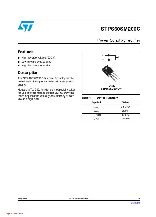
May 2011Doc ID 018819 Rev 11/7STPS60SM200CPower Schottky rectifierFeatures■High reverse voltage (200 V)■Low forward voltage drop ■High frequency operationDescriptionThe STPS60SM200C is a dual Schottky rectifier suited for high frequency switched-mode power supply.Housed in TO-247, this device is especially suited for use in telecom base station SMPS, providing these applications with a good efficiency at both low and high load.Table 1.Device summarySymbol Value I F(AV) 2 x 30 A V RRM 200 V T j (max)175 °C V F (typ)640 mVCharacteristics STPS60SM200C2/7Doc ID 018819 Rev 11 CharacteristicsWhen the two diodes 1 and 2 are used simultaneously:ΔT j (diode 1) = P(diode 1) x R th(j-c)(Per diode) + P(diode 2) x R th(c)To evaluate the conduction losses use the following equation: P = 0.58 x I F(AV) + 0.0037 x I F 2(RMS)Table 3.Thermal resistanceSymbol ParameterValue UnitR th(j-c)Junction to case Per diode 0.7°C/W Total0.5R th(c)Coupling0.3Table 4.Static electrical characteristics (per diode)Symbol ParameterTest conditions Min.Typ.Max.Unit I R (1)Reverse leakage currentT j = 25 °C V R = V RRM 0.05mAT j = 125 °C 613V F (2)Forward voltage dropT j = 25 °C I F = 7.5 A 0.670.70V T j = 125 °C 0.510.55T j = 25 °C I F = 15 A 0.730.77T j = 125 °C 0.570.61T j = 25 °C I F = 30 A0.790.83T j = 125 °C0.640.691.Pulse test: t p = 5 ms, δ < 2%2.Pulse test: t p = 380 µs, δ < 2%STPS60SM200CCharacteristicsDoc ID 018819 Rev 13/7Figure 1.Average forward power dissipation versus average forward current Figure 2.Average forward current versus ambient temperature (δ = 0.5)T= t /Tp t Figure 3.Non repetitive surge peak forward current versus overload duration Figure 4.Relative variation of thermalimpedance junction to case versus tFigure 5.Reverse leakage current versus reverse voltage applied Figure 6.Junction capacitance versus reverse voltage appliedCharacteristics STPS60SM200C4/7Doc ID 018819 Rev 1Figure 7.Forward voltage drop versus forward currentFigure 8.Forward voltage drop versus forward currentSTPS60SM200C Package informationDoc ID 018819 Rev 15/72 Package information●Epoxy meets UL94, V0●Cooling method: by conduction (C)●Recommended torque value: 0.55 to 1.0 N·mIn order to meet environmental requirements, ST offers these devices in different grades ofECOPACK ® packages, depending on their level of environmental compliance. ECOPACK ® specifications, grade definitions and product status are available at: . ECOPACK ® is an ST trademark.Ordering information STPS60SM200C6/7Doc ID 018819 Rev 13 Ordering information4 Revision historyTable 6.Ordering informationOrder code Marking Package Weight Base qty Delivery modeSTPS60SM200CWSTPS60SM200CWTO-2474.45 g30TubeTable 7.Document revision historyDate RevisionChanges17-May-20111First issue.STPS60SM200CPlease Read Carefully:Information in this document is provided solely in connection with ST products. STMicroelectronics NV and its subsidiaries (“ST”) reserve the right to make changes, corrections, modifications or improvements, to this document, and the products and services described herein at any time, without notice.All ST products are sold pursuant to ST’s terms and conditions of sale.Purchasers are solely responsible for the choice, selection and use of the ST products and services described herein, and ST assumes no liability whatsoever relating to the choice, selection or use of the ST products and services described herein.No license, express or implied, by estoppel or otherwise, to any intellectual property rights is granted under this document. If any part of this document refers to any third party products or services it shall not be deemed a license grant by ST for the use of such third party products or services, or any intellectual property contained therein or considered as a warranty covering the use in any manner whatsoever of such third party products or services or any intellectual property contained therein.UNLESS OTHERWISE SET FORTH IN ST’S TERMS AND CONDITIONS OF SALE ST DISCLAIMS ANY EXPRESS OR IMPLIED WARRANTY WITH RESPECT TO THE USE AND/OR SALE OF ST PRODUCTS INCLUDING WITHOUT LIMITATION IMPLIED WARRANTIES OF MERCHANTABILITY, FITNESS FOR A PARTICULAR PURPOSE (AND THEIR EQUIVALENTS UNDER THE LAWS OF ANY JURISDICTION), OR INFRINGEMENT OF ANY PATENT, COPYRIGHT OR OTHER INTELLECTUAL PROPERTY RIGHT. UNLESS EXPRESSLY APPROVED IN WRITING BY AN AUTHORIZED ST REPRESENTATIVE, ST PRODUCTS ARE NOT RECOMMENDED, AUTHORIZED OR WARRANTED FOR USE IN MILITARY, AIR CRAFT, SPACE, LIFE SAVING, OR LIFE SUSTAINING APPLICATIONS, NOR IN PRODUCTS OR SYSTEMS WHERE FAILURE OR MALFUNCTION MAY RESULT IN PERSONAL INJURY, DEATH, OR SEVERE PROPERTY OR ENVIRONMENTAL DAMAGE. ST PRODUCTS WHICH ARE NOT SPECIFIED AS "AUTOMOTIVE GRADE" MAY ONLY BE USED IN AUTOMOTIVE APPLICATIONS AT USER’S OWN RISK.Resale of ST products with provisions different from the statements and/or technical features set forth in this document shall immediately void any warranty granted by ST for the ST product or service described herein and shall not create or extend in any manner whatsoever, any liability of ST.ST and the ST logo are trademarks or registered trademarks of ST in various countries.Information in this document supersedes and replaces all information previously supplied.The ST logo is a registered trademark of STMicroelectronics. All other names are the property of their respective owners.© 2011 STMicroelectronics - All rights reservedSTMicroelectronics group of companiesAustralia - Belgium - Brazil - Canada - China - Czech Republic - Finland - France - Germany - Hong Kong - India - Israel - Italy - Japan - Malaysia - Malta - Morocco - Philippines - Singapore - Spain - Sweden - Switzerland - United Kingdom - United States of AmericaDoc ID 018819 Rev 17/7分销商库存信息: STMSTPS60SM200CW。
STS3DNE60L;中文规格书,Datasheet资料
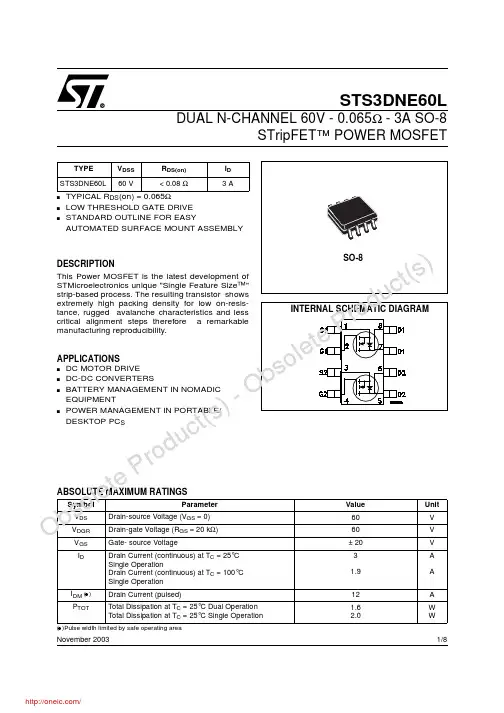
1/8November 2003STS3DNE60LDUAL N-CHANNEL 60V -0.065Ω -3A SO-8STripFET™POWERMOSFETs TYPICAL R DS (on)=0.065Ωs LOW THRESHOLD GATE DRIVE sSTANDARD OUTLINE FOR EASYAUTOMATED SURFACE MOUNT ASSEMBLYDESCRIPTIONThis Power MOSFET is the latest development of STMicroelectronics unique "Single Feature Size™"strip-based process.The resulting transistor shows extremely high packing density for low on-resis-tance,rugged avalanche characteristics and less critical alignment steps therefore a remarkable manufacturing reproducibility.APPLICATIONSs DC MOTOR DRIVE s DC-DC CONVERTERSs BATTERY MANAGEMENT IN NOMADIC EQUIPMENTs POWER MANAGEMENT IN PORTABLE/DESKTOP PC SABSOLUTE MAXIMUM RATINGS( )Pulsewidth limited by safe operating areaTYPE V DSS R DS(on)I D STS3DNE60L60V<0.08Ω3ASymbol ParameterValue Unit V DS Drain-source Voltage (V GS =0)60V V DGR Drain-gate Voltage (R GS =20k Ω)60V V GS Gate-source Voltage±20V I DDrain Current (continuous)at T C =25°C Single OperationDrain Current (continuous)at T C =100°C Single Operation 31.9A A I DM ( )Drain Current (pulsed)12A P TOTTotal Dissipation at T C =25°C Dual Operation Total Dissipation at T C =25°C Single Operation1.62.0W W l s Ob so e t ePr od u c t () -l t l c )Ob so e t ePr od u c (s )- O bs o e t eP r od u t (sSTS3DNE60L2/8THERMAL DATA(*)Mounted on FR-4Board (t ≤ 10 sec)ELECTRICAL CHARACTERISTICS (TCASE =25°C UNLESS OTHERWISE SPECIFIED)OFFON (1)DYNAMICRthj-amb(*)Thermal Resistance Junction-amb Max Single Operation (*)Thermal Resistance Junction-amb Max Dual Operation 62.578°C/W °C/W T j Max.Operating Junction Temperature 150°C T stgStorage Temperature–55to 150°CSymbol ParameterTest ConditionsMin.Typ.Max.Unit V (BR)DSS Drain-sourceBreakdown Voltage I D =250µA,V GS =060V I DSS Zero Gate VoltageDrain Current (V GS =0)V DS =Max Rating1µA V DS =Max Rating,T C =125°C 10µA I GSSGate-body Leakage Current (V DS =0)V GS =±20V±100nASymbol ParameterTest ConditionsMin.Typ.Max.Unit V GS(th)Gate Threshold Voltage V DS =V GS ,I D =250µA 1V R DS(on)Static Drain-source On ResistanceV GS =10V,I D =1.5A V GS =4.5V,I D =1.5A0.0650.080.080.1ΩΩSymbol ParameterTest ConditionsMin.Typ.Max.Unit g fs (1)Forward Transconductance V DS =15V ,I D =1.5A5S C iss Input Capacitance V DS =25V,f =1MHz,V GS =0815pF C oss Output Capacitance 125pF C rssReverse Transfer Capacitance40pFs l u )O() -O bs o e t eP r od c t(s3/8STS3DNE60LELECTRICAL CHARACTERISTICS (CONTINUED)SWITCHING ONSWITCHING OFFSOURCE DRAIN DIODENote: 1.Pulsed:Pulse duration =300µs,duty cycle 1.5%.2.Pulse width limited by safe operating area.Symbol ParameterTest ConditionsMin.Typ.Max.Unit t d(on)t r Turn-on Delay Time Rise TimeV DD =30V,I D =3A R G =4.7ΩV GS =5V (see test circuit,Figure 3)2030ns ns Q g Q gs Q gdTotal Gate Charge Gate-Source Charge Gate-Drain ChargeV DD =24V,I D =3A,V GS =4.5V13.563.5nC nC nCSymbol ParameterTest ConditionsMin.Typ.Max.Unit t r(off)t f t cOff-voltage Rise Time Fall TimeCross-over TimeV DD =48V,I D =3A R G =4.7Ω,V GS =5V (see test circuit,Figure 5)121632ns ns nsSymbol ParameterTest ConditionsMin.Typ.Max.Unit I SD Source-drain Current 3A I SDM (1)Source-drain Current (pulsed)12A V SD (2)Forward On Voltage I SD =3A,V GS =0 1.2V t rr Q rr I RRMReverse Recovery Time Reverse Recovery Charge Reverse Recovery CurrentI SD =3A,di/dt =100A/µs,V DD =30V,T j =150°C (see test circuit,Figure 5)601304ns nC AO-O STS3DNE60L4/8.Tranconductancellc Ob so e t eP-O bs o e t eP r od u t (5/8STS3DNE60LSource-drain Diode Forward Characteristics)osSTS3DNE60L6/8Fig.5:Test Circuit For Inductive Load Switching And Diode Recovery TimesFig.4:Gate Charge test CircuitFig.2:Unclamped Inductive WaveformFig.1:Unclamped Inductive Load Test CircuitFig.3:Switching Times Test Circuit For Resistive LoadSTS3DNE60L7/8l slc)O b s oe t eP ro du ct()-O bs oe t eP ro dut(sSTS3DNE60L8/8Information furnished is believed to be accurate and reliable. However, STMicroelectronics assumes no responsibility for the consequences of use of such information nor for any infringement of patents or other rights of third parties which may result from its use. No license is granted by implication or otherwise under any patent or patent rights of STMicroelectronics. Specifications mentioned in this publication are subject to change without notice. This publication supersedes and replaces all information previously supplied. STMicroelectronics products are not authorized for use as critical components in life support devices or systems without express written approval of STMicroelectronics.© The ST logo is a registered trademark of STMicroelectronics© 2003 STMicroelectronics - Printed in Italy - All Rights ReservedSTMicroelectronics GROUP OF COMPANIESAustralia - Brazil - Canada - China - Finland - France - Germany - Hong Kong - India - Israel - Italy - Japan - Malaysia - Malta - Morocco Singapore - Spain - Sweden - Switzerland - United Kingdom - United States.© 分销商库存信息: STMSTS3DNE60L。
VISHAY VLMF31. 数据手册
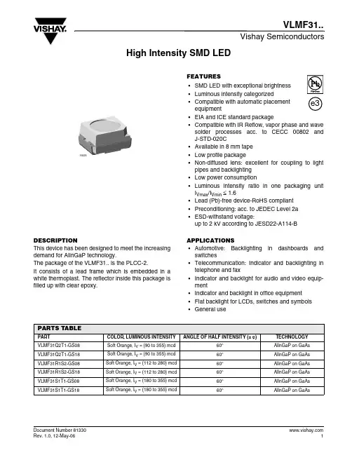
Vishay SemiconductorsVLMF31..High Intensity SMD LEDFEATURES•SMD LED with exceptional brightness •Luminous intensity categorized•Compatible with automatic placement equipment•EIA and ICE standard package•Compatible with IR Reflow, vapor phase and wave solder processes acc. to CECC 00802 and J-STD-020C•Available in 8 mm tape •Low profile package•Non-diffused lens: excellent for coupling to light pipes and backlighting •Low power consumption •Luminous intensity ratio in one packaging unit I Vmax /I Vmin ≤ 1.6•Lead (Pb)-free device-RoHS compliant •Preconditioning: acc. to JEDEC Level 2a •ESD-withstand voltage:up to 2 kV according to JESD22-A114-B19225DESCRIPTIONThis device has been designed to meet the increasing demand for AlInGaP technology.The package of the VLMF31.. is the PLCC-2.It consists of a lead frame which is embedded in a white thermoplast. The reflector inside this package is filled up with clear epoxy.APPLICATIONS •Automotive: Backlighting in dashboards and switches•Telecommunication: Indicator and backlighting in telephone and fax•Indicator and backlight for audio and video equip-ment•Indicator and backlight in office equipment •Flat backlight for LCDs, switches and symbols •General usePARTS TABLEPARTCOLOR, LUMINOUS INTENSITY ANGLE OF HALF INTENSITY (± ϕ)TECHNOLOGY VLMF31Q2T1-GS08Soft Orange, I V = (90 to 355) mcd 60°AllnGaP on GaAs VLMF31Q2T1-GS18Soft Orange, I V = (90 to 355) mcd 60°AllnGaP on GaAs VLMF31R1S2-GS08Soft Orange, I V = (112 to 280) mcd 60°AllnGaP on GaAs VLMF31R1S2-GS18Soft Orange, I V = (112 to 280) mcd 60°AllnGaP on GaAs VLMF31S1T1-GS08Soft Orange, I V = (180 to 355) mcd 60°AllnGaP on GaAs VLMF31S1T1-GS18Soft Orange, I V = (180 to 355) mcd60°AllnGaP on GaAsVishay Semiconductors VLMF31..Note:1) Tamb = 25°C unless otherwise specified2) Driving the LED in reverse direction is suitable for a short term application Note:1) Tamb = 25°C unless otherwise specified2) in one Packing Unit IVmax/I Vmin≤ 1.6Note:Luminous intensity is tested at a current pulse duration of 25 ms and an accuracy of ± 11 %.The above type numbers represent the order groups which include only a few brightness groups. Only one group will be shipped on each reel (there will be no mixing of two groups on each reel).In order to ensure availability, single brightness groups will not be or-derable.In a similar manner for colors where wavelength groups are mea-sured and binned, single wavelength groups will be shipped on any one reel. In order to ensure availability, single wavelength groups will not be orderable.Note:Wavelengths are tested at a current pulse duration of 25 ms and an accuracy of ± 1 nm.ABSOLUTE MAXIMUM RATINGS1), VLMF31..PARAMETER TEST CONDITION SYMBOL VALUE UNIT Reverse voltage2)V R5V DC Forward current T amb≤ 85°C I F30mA Surge forward current t p≤ 10 µs I FSM0.1A Power dissipation P V80mW Junction temperature T j125°C Operating temperature range T amb- 40 to + 100°C Storage temperature range T stg- 40 to + 100°CThermal resistance junction/ ambient mounted on PC board(pad size > 16 mm2)R thJA400K/WOPTICAL AND ELECTRICAL CHARACTERISTICS1), VLMF31.., SOFT ORANGEPARAMETER TEST CONDITION PART SYMBOL MIN TYP.MAX UNIT Luminous intensity2)I F = 20 mA VLMF31Q2T1I V90355mcdVLMF31R1S2I V112280mcdVLMF31S1T1I V180355mcd Dominant wavelength I F = 20 mAλd598605611nm Peak wavelength I F = 20 mAλp610nm Angle of half intensity I F = 20 mAϕ± 60deg Forward voltage I F = 20 mA V F 2.0 2.6V Reverse voltage I R = 10 µA V R5V Junction capacitance V R = 0, f = 1 MHz C j15pFLUMINOUS INTENSITY CLASSIFICATIONGROUP LIGHT INTENSITY [MCD]STANDARD OPTIONAL MIN MAXP 14556 25671Q 17190 290112R 1112140 2140180S 1180224 2224280T 12803552355450CROSSING TABLEVISHAY OSRAMVLMF31Q2T1LOT676-Q2T1VLMF31R1S2LOT676-R1S2VLMF31S1T1LOT676-S1T1COLOR CLASSIFICATIONGROUP SOFT ORANGEDOM. WAVELENGTH (NM)MIN. MAX.159860126006033602605460460756066096608611Vishay SemiconductorsVLMF31..TYPICAL CHARACTERISTICST amb = 25°C unless otherwise specifiedFigure 1. Forward Current vs. Ambient TemperatureFigure 3. Rel. Luminous Intensity vs. Angular Displacement 05101520253035400102030405060708090100T am b - Am b ient Temperat u re (°C)16615I - F o r w a r d C u r r e n t (m A )F0.40.200.20.40.695 103190.60.90.80°30°10°20°40°50°60°70°80°0.71.0I v r e l -R e l a t i v e L u m i n o u s I n t e n s i t yFigure 4. Relative Intensity vs. WavelengthFigure 5. Forward Current vs. Forward VoltageFigure6. Relative Luminous Intensity vs. Forward Current1101001.01.52.0 2.53.0V F -For w ard V oltage (V )95 10878F I -F o r w a r d C u r r e n t (m A )Vishay SemiconductorsVLMF31..PACKAGE DIMENSIONS IN MMFigure7. Rel. Luminous Intensity vs. Ambient Temperature Figure8. Forward Voltage vs. Ambient TemperatureVishay SemiconductorsVLMF31..METHOD OF TAPING/POLARITY AND TAPE AND REEL SMD LED (VLM3 - SERIES)Vishay’s LEDs in SMD packages are available in an antistatic 8 mm blister tape (in accordance with DIN IEC 40 (CO) 564) for automatic component inser-tion. The blister tape is a plastic strip with impressed component cavities, covered by a top tape.TAPING OF VLM.3..REEL PACKAGE DIMENSION IN MM FOR SMD LEDS, TAPE OPTION GS08(= 1500 PCS.)REEL PACKAGE DIMENSION IN MM FOR SMD LEDS, TAPE OPTION GS18(= 8000 PCS.) PREFEREDFigure9. Tape dimensions in mm for PLCC-2Figure 10. Reel dimensions - GS08Figure 11. Reel dimensions - GS18Vishay SemiconductorsVLMF31..SOLDERING PROFILEBARCODE-PRODUCT-LABEL EXAMPLE:A)Type of component B)Manufacturing PlantC)SEL - Selection Code (Bin):e.g.: Q2 = Code for Luminous Intensity Group 1 = Code for Color Group D)Date Code year/weekE)Day Code (e.g. 3: Wednesday)F)Batch No.G)Total quantity H)Company CodeFigure 12. Vishay Leadfree Reflow Soldering Profile(acc. to J-STD-020C)Figure 13. Double wave soldering of opto devices (all packages)V ISHAYAHBC D E F GVishay SemiconductorsVLMF31..DRY PACKINGThe reel is packed in an anti-humidity bag to protect the devices from absorbing moisture during transpor-tation and storage.FINAL PACKINGThe sealed reel is packed into a cardboard box. A sec-ondary cardboard box is used for shipping purposes.RECOMMENDED METHOD OF STORAGEDry box storage is recommended as soon as the alu-minium bag has been opened to prevent moisture absorption. The following conditions should be observed, if dry boxes are not available:• Storage temperature 10°C to 30°C • Storage humidity ≤ 60 % RH max.After more than 672 hours under these conditions moisture content will be too high for reflow soldering.In case of moisture absorption, the devices will recover to the former condition by drying under the following condition:192 hours at 40°C + 5°C/ - 0°C and < 5 % RH (dry air/nitrogen) or96 hours at 60°C + 5°C and < 5 % RH for all device containers or24 hours at 100°C + 5°C not suitable for reel or tubes.An EIA JEDEC Standard JESD22-A112 Level 2a label is included on all dry bags.Example of JESD22-A112 Level 2a labelESD PRECAUTIONProper storage and handling procedures should be fol-lowed to prevent ESD damage to the devices espe-cially when they are removed from the Antistatic Shielding Bag. Electro-Static Sensitive Devices warn-ing labels are on the packaging.VISHAY SEMICONDUCTORS STANDARD BAR-CODE LABELSThe Vishay Semiconductors standard bar-code labels are printed at final packing areas. The labels are on each packing unit and contain Vishay Semiconductors specific data.VLMF31..Vishay SemiconductorsOZONE DEPLETING SUBSTANCES POLICY STATEMENTIt is the policy of Vishay Semiconductor GmbH to1.Meet all present and future national and international statutory requirements.2.Regularly and continuously improve the performance of our products, processes, distribution and operatingsystems with respect to their impact on the health and safety of our employees and the public, as well as their impact on the environment.It is particular concern to control or eliminate releases of those substances into the atmosphere which are known as ozone depleting substances (ODSs).The Montreal Protocol (1987) and its London Amendments (1990) intend to severely restrict the use of ODSs and forbid their use within the next ten years. Various national and international initiatives are pressing for an earlier ban on these substances.Vishay Semiconductor GmbH has been able to use its policy of continuous improvements to eliminate the use of ODSs listed in the following documents.1.Annex A, B and list of transitional substances of the Montreal Protocol and the London Amendments respectively2.Class I and II ozone depleting substances in the Clean Air Act Amendments of 1990 by the EnvironmentalProtection Agency (EPA) in the USA3.Council Decision 88/540/EEC and 91/690/EEC Annex A, B and C (transitional substances) respectively. Vishay Semiconductor G mbH can certify that our semiconductors are not manufactured with ozone depleting substances and do not contain such substances.We reserve the right to make changes to improve technical designand may do so without further notice.Parameters can vary in different applications. All operating parameters must be validated for each customer application by the customer. Should the buyer use Vishay Semiconductors products for any unintended or unauthorized application, the buyer shall indemnify Vishay Semiconductors against all claims, costs, damages, and expenses, arising out of, directly or indirectly, any claim of personal damage, injury or deathassociated with such unintended or unauthorized use.Vishay Semiconductor GmbH, P.O.B. 3535, D-74025 Heilbronn, GermanyLegal Disclaimer NoticeVishayNoticeSpecifications of the products displayed herein are subject to change without notice. Vishay Intertechnology, Inc., or anyone on its behalf, assumes no responsibility or liability for any errors or inaccuracies.Information contained herein is intended to provide a product description only. No license, express or implied, by estoppel or otherwise, to any intellectual property rights is granted by this document. Except as provided in Vishay's terms and conditions of sale for such products, Vishay assumes no liability whatsoever, and disclaims any express or implied warranty, relating to sale and/or use of Vishay products including liability or warranties relating to fitness for a particular purpose, merchantability, or infringement of any patent, copyright, or other intellectual property right. The products shown herein are not designed for use in medical, life-saving, or life-sustaining applications. Customers using or selling these products for use in such applications do so at their own risk and agree to fully indemnify Vishay for any damages resulting from such improper use or sale.。
STPS30100ST;中文规格书,Datasheet资料
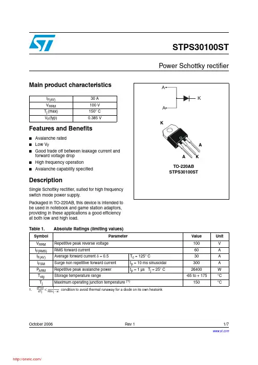
October 2006 Rev 11/7STPS30100STPower Schottky rectifierMain product characteristicsFeatures and Benefits■Avalanche rated ■Low V F■Good trade off between leakage current and forward voltage drop ■High frequency operation ■Avalanche capability specifiedDescriptionSingle Schottky rectifier, suited for high frequency switch mode power supply.Packaged in TO-220AB, this device is intended to be used in notebook and game station adaptors, providing in these applications a good efficiency at both low and high load.I F(AV)30 A V RRM 100 V T j (max)150° C V F (typ)0.385 VTable 1.Absolute Ratings (limiting values)Symbol ParameterValue Unit V RRM Repetitive peak reverse voltage 100V I F(RMS)RMS forward current60A I F(AV)Average forward current δ = 0.5T c = 125° C 30A I FSM Surge non repetitive forward current t p = 10 ms sinusoidal 300A P ARM Repetitive peak avalanche power t p = 1 µs T j = 25° C26400W T stg Storage temperature range-65 to + 175°C T jMaximum operating junction temperature (1)1. condition to avoid thermal runaway for a diode on its own heatsink150°CdPtot dTj---------------1Rth j a –()-------------------------<Characteristics STPS30100ST2/71 CharacteristicsTo evaluate the conduction losses use the following equation:P = 0.475 x I F(AV) + 0.006 x I F 2(RMS)Table 2.Thermal resistanceSymbol ParameterValue Unit R th(j-c)Junction to case1°C/WTable 3.Static electrical characteristics (per diode)SymbolParameterTest Conditions Min.Typ.Max.Unit I R (1)1.Pulse test: t p = 5 ms, δ < 2%Reverse leakage currentT j = 25° CV R = V RRM175µA T j = 125° C 2050mA T j = 25° C V R = 70 V 60µA T j = 125° C 1020mAV F (2)2.Pulse test: t p = 380 µs, δ < 2%Forward voltage dropT j = 25° C I F = 5 A0.475VT j = 125° C 0.385T j = 25° C I F = 10 A0.555T j = 125° C 0.475T j = 25° C I F = 15 A 0.6200.660T j = 125° C 0.5250.565T j = 25° C I F = 30 A0.7400.800T j = 125° C0.6050.655STPS30100STCharacteristics3/7Figure 1.Conduction losses versus average Figure 2.Average forward current versusTδ=t /Tp tTδ=t p /Tt Figure 3.Normalized avalanche power derating versus pulse durationFigure 4.Normalized avalanche power derating versus junction Figure 5.Non repetitive surge peak forward current versus overload duration Figure 6.Relative variation of thermalimpedance junction to case versusCharacteristicsSTPS30100ST4/7Figure 7.Reverse leakage current versusreverse voltage applied (typicalFigure 8.Junction capacitance versus reverse voltage applied (typical Figure 9.Forward voltage drop versusFigure 10.Forward voltage drop versusSTPS30100ST Package Information5/72 Package InformationEpoxy meets UL94,V0In order to meet environmental requirements, ST offers these devices in ECOP ACK®packages. These packages have a lead-free second level interconnect. The category of second level interconnect is marked on the package and on the inner box label, in compliance with JEDEC Standard JESD97. The maximum ratings related to soldering conditions are also marked on the inner box label. ECOP ACK is an ST trademark. ECOP ACK specifications are available at: .Ordering Information STPS30100ST6/73 Ordering Information4 Revision HistoryOrdering type Marking Package Weight Base qtyDelivery modeSTPS30100STSTPS30100STTO-220AB2.23 g50TubeDate RevisionChanges24-Oct-20061First issueSTPS30100STPlease Read Carefully:Information in this document is provided solely in connection with ST products. STMicroelectronics NV and its subsidiaries (“ST”) reserve the right to make changes, corrections, modifications or improvements, to this document, and the products and services described herein at any time, without notice.All ST products are sold pursuant to ST’s terms and conditions of sale.Purchasers are solely responsible for the choice, selection and use of the ST products and services described herein, and ST assumes no liability whatsoever relating to the choice, selection or use of the ST products and services described herein.No license, express or implied, by estoppel or otherwise, to any intellectual property rights is granted under this document. If any part of this document refers to any third party products or services it shall not be deemed a license grant by ST for the use of such third party products or services, or any intellectual property contained therein or considered as a warranty covering the use in any manner whatsoever of such third party products or services or any intellectual property contained therein.UNLESS OTHERWISE SET FORTH IN ST’S TERMS AND CONDITIONS OF SALE ST DISCLAIMS ANY EXPRESS OR IMPLIED WARRANTY WITH RESPECT TO THE USE AND/OR SALE OF ST PRODUCTS INCLUDING WITHOUT LIMITATION IMPLIED WARRANTIES OF MERCHANTABILITY, FITNESS FOR A PARTICULAR PURPOSE (AND THEIR EQUIVALENTS UNDER THE LAWS OF ANY JURISDICTION), OR INFRINGEMENT OF ANY PATENT, COPYRIGHT OR OTHER INTELLECTUAL PROPERTY RIGHT. UNLESS EXPRESSLY APPROVED IN WRITING BY AN AUTHORIZED ST REPRESENTATIVE, ST PRODUCTS ARE NOT RECOMMENDED, AUTHORIZED OR WARRANTED FOR USE IN MILITARY, AIR CRAFT, SPACE, LIFE SAVING, OR LIFE SUSTAINING APPLICATIONS, NOR IN PRODUCTS OR SYSTEMS WHERE FAILURE OR MALFUNCTION MAY RESULT IN PERSONAL INJURY, DEATH, OR SEVERE PROPERTY OR ENVIRONMENTAL DAMAGE. ST PRODUCTS WHICH ARE NOT SPECIFIED AS "AUTOMOTIVE GRADE" MAY ONLY BE USED IN AUTOMOTIVE APPLICATIONS AT USER’S OWN RISK.Resale of ST products with provisions different from the statements and/or technical features set forth in this document shall immediately void any warranty granted by ST for the ST product or service described herein and shall not create or extend in any manner whatsoever, any liability of ST.ST and the ST logo are trademarks or registered trademarks of ST in various countries.Information in this document supersedes and replaces all information previously supplied.The ST logo is a registered trademark of STMicroelectronics. All other names are the property of their respective owners.© 2006 STMicroelectronics - All rights reservedSTMicroelectronics group of companiesAustralia - Belgium - Brazil - Canada - China - Czech Republic - Finland - France - Germany - Hong Kong - India - Israel - Italy - Japan - Malaysia - Malta - Morocco - Singapore - Spain - Sweden - Switzerland - United Kingdom - United States of America7/7分销商库存信息: STMSTPS30100ST。
STTH6003CW;中文规格书,Datasheet资料
STTH6003TV/CWOctober 1999 - Ed: 5CHIGH FREQUENCY SECONDARY RECTIFIER®Dual rectifiers suited for Switch Mode Power Supply and high frequency DC to DC converters.Packaged either in ISOTOP or in TO-247, this device is intended for use in low voltage, high frequency inverters, free wheeling operation,welding equipments and telecom power supplies.DESCRIPTIONCOMBINES HIGHEST RECOVERY AND VOLTAGE PERFORMANCEULTRA-FAST, SOFT AND NOISE-FREE RECOVERYINSULATED PACKAGE: ISOTOP Insulation voltage: 2500 V RMS Capacitance: < 45 pFLOW INDUCTANCE AND LOW CAPACI-TANCE ALLOW SIMPLIFIED LAYOUT FEATURES AND BENEFITSSymbol ParameterValue Unit V RRM Repetitive peak reverse voltage 300V I F(RMS)RMS forward current ISOTOP 100A I F(RMS)RMS forward current TO-24760A I F(AV)Average forward current ISOTOPTc = 95°C δ = 0.5Per diode Per device 3060A TO-247Tc =135°C δ = 0.5Per diode Per device 3060A I FSM Surge non repetitive forward current.ISOTOP tp = 10 ms sinusoidal 400A TO-247tp = 10 ms sinusoidal 300A I RSMNon repetitive peak reverse current tp =100 µs square4A T stg Storage temperature rangeISOTOP - 55 to + 150°C TO-247- 65 to + 175°C TjMaximum operating junction temperatureISOTOP 150°C TO-247175°CABSOLUTE RATINGS (limiting values, per diode)I F(AV) 2 x 30 A V RRM 300 V V F (max) 1 V trr (max)55 nsMAJOR PRODUCT CHARACTERISTICSA1K1K2A2A1A2K1K2ISOTOP ™STTH6003TV ISOTOP is a registered trademark of STMicroelectronicsA1K A2A1A2KTO-247STTH6003CW1/6Symbol Parameter Tests conditionsMin.Typ.Max.Unit I R *Reverse leakage currentV R = 300 VTj = 25°C 60µATj = 125°C60600V F **Forward voltage dropI F = 30 ATj = 25°C 1.25V Tj = 125°C0.851Pulse test : * tp = 5 ms, δ < 2 % ** tp = 380 µs, δ < 2%To evaluate the maximum conduction losses use the following equation:P = 0.75 x I F(AV) + 0.008 x I F 2(RMS)STATIC ELECTRICAL CHARACTERISTICS (per diode)Symbol ParameterValue Unit R th (j-c)Junction to caseISOTOP Per diodeTotal 1.40.75°C/WTO-247Per diode Total 10.55R th (c)Coupling0.1When the diodes 1 and 2 are used simultaneously:∆Tj (diode 1) = P (diode 1) x R th(j-c) (per diode) + P (diode 2) x R th(C)THERMAL RESISTANCES Symbol Tests conditionsMin.Typ.Max.Unit trrI F = 0.5 A Irr = 0.25 A I R = 1A Tj = 25°C40nsI F= 1 A dI F /dt = - 50 A/µs V R = 30 V 55tfr I F = 30 A dI F /dt = 200 A/µs Tj = 25°C 350ns V FP V FR = 1.1 x V F max.5V S factor Vcc = 200 V I F = 30 A Tj = 125°C0.3-I RMdI F /dt = 200 A/µs11A RECOVERY CHARACTERISTICS STTH6003TV/CW2/65101520253035400510152025303540IF(av) (A)P1(W)Tδ=tp/Ttpδ= 1δ= 0.5δ= 0.2δ= 0.1δ= 0.05Fig. 1: Conduction losses versus average current (per diode).0.20.40.60.81.01.21.41.61.82.02.22.42.6110100VFM(V)IFM(A)Tj=125°C T ypical valuesTj=25°C Maximum valuesTj=125°C Maximum valuesFig. 2: Forward voltage drop versus forward current (maximum values , per diode).05010015020025030035040045050020406080100120140160180trr(ns)VR=200V Tj=125°CIF=2*IF(av)IF=IF(av)IF=0.5*IF(av)dIF/dt(A/µs)Fig. 5: Reverse recovery time versus dI F /dt (90%confidence, per diode).50100150200250300350400450500246810121416182022dIF/dt(A/µs)IRM(A)VR=200V Tj=125°CIF=2*IF(av)IF=IF(av)IF=0.5*IF(av)Fig. 4: Peak reverse recovery current versus dI F /dt (90% confidence, per diode).1E-31E-21E-11E+01E+10.00.20.40.60.81.0tp(s)Zth(j-c)/Rth(j-c)Tδ=tp/TtpSingle pulse δ= 0.5δ= 0.2δ= 0.1Fig. 3a: Relative variation of thermal impedance junction to case versus pulse duration (ISOTOP).1E-41E-31E-21E-11E+00.00.20.40.60.81.0Zth(j-c)/Rth(j-c)Tδ=tp/Ttptp(s)Single pulseδ= 0.5δ= 0.2δ= 0.1Fig. 3b: Relative variation of thermal impedance junction to case versus pulse duration (TO-247).STTH6003TV/CW3/62550751001250.00.20.40.60.81.01.21.41.61.82.02.22.4Tj(°C)IRMS factorFig. 7: Relative variation of dynamic parameters versus junction temperature (reference: Tj = 125°C).50100150200250300350400450500246810VFP(V)IF=IF(av)Tj=125°CdIF/dt(A/µs)Fig. 8: Transient peak forward voltage versus dI F /dt (90% confidence, per diode).050100150200250300350400450500100200300400500tfr(ns)IF=IF(av)VFR=1.1*VFmaxTj=125°CdIF/dt(A/µs)Fig. 9: Forward recovery time versus dI F /dt (90%confidence, per diode).0501001502002503003504004505000.00.10.20.30.40.50.6S factor VR=200V Tj=125°CdIF/dt(A/µs)Fig. 6: Softness factor (tb/ta) versus dI F /dt (typical values, per diode).STTH6003TV/CW4/6PACKAGE MECHANICAL DATA ISOTOPREF.DIMENSIONS Millimeters Inches Min.Max.Min.Max.A11.8012.200.4650.480 A18.909.100.3500.358 B7.88.200.3070.323 C0.750.850.0300.033 C2 1.95 2.050.0770.081 D37.8038.20 1.488 1.504 D131.5031.70 1.240 1.248 E25.1525.500.990 1.004 E123.8524.150.9390.951 E224.80 typ.0.976 typ.G14.9015.100.5870.594 G112.6012.800.4960.504 G2 3.50 4.300.1380.169 F 4.10 4.300.1610.169 F1 4.60 5.000.1810.197 P 4.00 4.300.1570.69P1 4.00 4.400.1570.173 S30.1030.30 1.185 1.193STTH6003TV/CW5/6Information furnished is believed to be accurate and reliable. However, STMicroelectronics assumes no responsibility for the consequences of use of such information nor for any infringement of patents or other rights of third parties which may result from its use. No license is granted by implication or otherwise under any patent or patent rights of STMicroelectronics. Specifications mentioned in this publication are subject to change without notice. This publication supersedes and replaces all information previously supplied.STMicroelectronics products are not authorized for use as critical components in life support devices or systems without express written ap-proval of STMicroelectronics.The ST logo is a registered trademark of STMicroelectronics © 1999 STMicroelectronics - Printed in Italy - All rights reserved.STMicroelectronics GROUP OF COMPANIESAustralia - Brazil - China - Finland - France - Germany - Hong Kong - India - Italy - Japan - MalaysiaMalta - Morocco - Singapore - Spain - Sweden - Switzerland - United Kingdom - U.S.A.PACKAGE MECHANICAL DATA TO-247F2F1V2L4L2L1L3DLL5MEHVVADia.F3F4G = =F(x3)REF.DIMENSIONSMillimeters Inches Min.Typ.Max.Min.Typ.Max.A 4.85 5.150.1910.203D 2.20 2.600.0860.102E 0.400.800.0150.031F 1.00 1.400.0390.055F1 3.000.118F2 2.000.078F3 2.00 2.400.0780.094F4 3.00 3.400.1180.133G 10.900.429H 15.4515.750.6080.620L 19.8520.150.7810.793L1 3.70 4.300.1450.169L218.500.728L314.2014.800.5590.582L434.60 1.362L5 5.500.216M 2.00 3.000.0780.118V 5°5°V260°60°Dia. 3.55 3.650.1390.143Ordering code Marking Package Weight Base qty Delivery modeSTTH6006TV1STTH6006TV ISOTOP 27gwithout screws10with screwsTubeSTTH6006CW STTH6006CW TO-247 4.36g30TubeCooling method: by conduction (C)Recommended torque value (ISOTOP): 1.3 N.m.Recommended torque value (TO-247°: 0.8 N.m.Maximum torque value (ISOTOP): 1.5 N.m.Maximum torque value (TO-247): 1.0 N.m.Epoxy meets UL 94,V0STTH6003TV/CW6/6分销商库存信息: STMSTTH6003CW。
WM产品规格书
样 品 确 认 书SAMPLE REPORT FOR APPROVAL客户名称CUSTOMER 产品名称开关电源PRODUCT NAME 型 号WMAH250T120MODEL DETAIL 规 格SPECIFICATION 料 号PART NO 供 应 商深圳市西磁科技有限公司备注:请贵公司将样品确认结果签字盖章后回传。
目 录一、产品概述----------------------------------------------------------------------------------------2深圳市西磁科技有限公司地址:深圳市南山区丽山路民企科技园3栋5搂TEL :6 FAX :6二、产品主要---------------------------------------------------------------------------------------- 2三、引用标准及规范----------------------------------------------------------------------------- 2四、环境条件---------------------------------------------------------------------------------------- 2五、电气特性---------------------------------------------------------------------------------------- 3六、保护特性--------------------------------------------------------------------------------------- 3七、安规要求---------------------------------------------------------------------------------------47-1 绝缘强度和绝缘阻抗------------------------------------------------------------------- 47-2 漏电流------------------------------------------------------------------------------------- 4八、产品安装、使用说明8-2 运输----------------------------------------------------------------------------------- 48-3 储存----------------------------------------------------------------------------------- 4九、包装、运输、储存十、外观尺寸10-1外形尺寸------------------------------------------------------------------------------ 510-3定位尺寸及外观图------------------------------------------------------------------- 510-3 端子定义----------------------------------------------------------------------------- 5一、产品概述1-1.低成本和高可靠性。
DPtech LSW2300系列以太网交换机安装手册v1.2
DPtech LSW2300系列以太网交换机 安装手册
i
DPtech LSW2300系列以太网交换机安装手册
杭州迪普科技股份有限公司为客户提供全方位的技术支 持。 通过杭州迪普科技股份有限公司代理商购买产品的用 户,请直接与销售代理商联系;直接向杭州迪普科技股 份有限公司购买产品的用户,可直接与公司联系。 杭州迪普科技股份有限公司 地址: 杭州市滨江区通和路68号中财大厦6层 邮编:310052
1.1 产品概述 .................................................................................................................................. 1-1 1.2 产品型号及规格介绍 .............................................................................................................. 1-1 1.3 前后面板介绍 .......................................................................................................................... 1-3 1.3.1 LSW2300-8T4GP-I/LSW2300-8T4GP-I-DC产品外观 ....................................................... 1-3 1.3.2 LSW2300-8GT4GP-I/LSW2300-8GT4GP-I-DC产品外观.................................................. 1-7 1.3.3 LSW2300-16GT2GP-I/ LSW2300-16GT2GP-I-DC 产品外观 .......................................... 1-11 1.4 端口介绍 ................................................................................................................................ 1-14 1.4.1 CONSOLE口 ......................................................................................................................... 1-14 1.4.2 百兆/千兆以太网电接口 .................................................................................................... 1-15 1.4.3 SFP口 .................................................................................................................................. 1-17
V30100PW-M34W;中文规格书,Datasheet资料
Document Number: 89178For technical questions within your region, please contact one of the following:Dual High-Voltage Trench MOS Barrier Schottky RectifierUltra Low V F = 0.58 V at I F = 8 AV30100PWVishay General SemiconductorFEATURES•Trench MOS Schottky technology•Low forward voltage drop, low power losses •High efficiency operation•Solder dip 275 °C max. 10 s, per JESD 22-B106•Compliant to RoHS directive 2002/95/EC and in accordance to WEEE 2002/96/EC•Halogen-free according to IEC 61249-2-21 definitionTYPICAL APPLICATIONSFor use in high frequency converters, switching power supplies, freewheeling diodes, OR-ing diode, dc-to-dc converters and reverse battery protection.MECHANICAL DATACase: TO-3PWMolding compound meets UL 94 V-0 flammability rating Base P/N-M3 - halogen-free and RoHS compliant,commercial gradeTerminals: Matte tin plated leads, solderable per J-STD-002 and JESD 22-B102M3 suffix meets JESD 201 class 1A whisker test Polarity: As markedMounting Torque: 10 in-lbs maximumPRIMARY CHARACTERISTICSI F(AV) 2 x 15 A V RRM 100 V I FSM120 A E AS at L = 60 mH 150 mJ V F at I F = 15 A 0.68 V T J max.150 °CMAXIMUM RATINGS (T A = 25°C unless otherwise noted)PARAMETERSYMBOL V30100PWUNIT Maximum repetitive peak reverse voltage V RRM 100V Maximum average forward rectified current (fig. 1)per device I F(AV)30A per diode15Peak forward surge current 8.3 ms single half sine-wave superimposed on rated load per diodeI FSM 120A Non-repetitive avalanche energy at T J = 25 °C, L = 60 mH per diode E AS 150mJ Peak repetitive reverse current at t p = 2 μs, 1 kHz,T J = 38 °C ± 2 °C per diode I RRM 1.0A Voltage rate of change (rated V R )dV/dt 10 000V/μs Operating junction and storage temperature rangeT J , T STG- 40 to + 150°C For technical questions within your region, please contact one of the following:Document Number: 89178V30100PWVishay General SemiconductorNotes(1)Pulse test: 300 μs pulse width, 1 % duty cycle (2)Pulse test: Pulse width ≤ 40 msRATINGS AND CHARACTERISTICS CURVES(T A = 25 °C unless otherwise noted)Fig. 1 - Forward Current Derating Curve Fig. 2 - Forward Power Loss Characteristics Per DiodeELECTRICAL CHARACTERISTICS (T A = 25°C unless otherwise noted)PARAMETER TEST CONDITIONS SYMBOL TYP.MAX.UNIT Breakdown voltageI R = 1.0 mA T J = 25 °C V BR100 (minimum)-VInstantaneous forward voltage per diodeI F = 8 AT J = 25 °CV F (1)0.64-V I F = 15 A 0.830.91I F = 8 A T J = 125 °C 0.58-I F = 15 A 0.680.76Reverse current per diodeV R = 70 VT J = 25 °C I R (2) 6.3-μA T J = 125 °C 4.4-mA V R = 100 VT J = 25 °C 22450μA T J = 125 °C1026mATHERMAL CHARACTERISTICS (T A = 25°C unless otherwise noted)PARAMETERSYMBOL V30100PWUNIT Typical thermal resistanceper diode R θJC2.0°C/Wper device1.4ORDERING INFORMATION (Example)PACKAGE PREFERRED P/N UNIT WEIGHT (g)PACKAGE CODEBASE QUANTITYDELIVERY MODETO-3PWV30100PW-M3/4W4.54W30/tubeTubeDocument Number: 89178For technical questions within your region, please contact one of the following:V30100PWVishay General SemiconductorFig. 3 - Typical Instantaneous Forward Characteristics Per Diode Fig. 4 - Typical Reverse Characteristics Per Diode Fig. 5 - Typical Junction Capacitance Per DiodeFig. 6 - Typical Transient Thermal Impedance Per DiodePACKAGE OUTLINE DIMENSIONS in inches (millimeters)Legal Disclaimer Notice VishayDisclaimerALL PRODU CT, PRODU CT SPECIFICATIONS AND DATA ARE SU BJECT TO CHANGE WITHOU T NOTICE TO IMPROVE RELIABILITY, FUNCTION OR DESIGN OR OTHERWISE.Vishay Intertechnology, Inc., its affiliates, agents, and employees, and all persons acting on its or their behalf (collectively,“Vishay”), disclaim any and all liability for any errors, inaccuracies or incompleteness contained in any datasheet or in any other disclosure relating to any product.Vishay makes no warranty, representation or guarantee regarding the suitability of the products for any particular purpose or the continuing production of any product. To the maximum extent permitted by applicable law, Vishay disclaims (i) any and all liability arising out of the application or use of any product, (ii) any and all liability, including without limitation special, consequential or incidental damages, and (iii) any and all implied warranties, including warranties of fitness for particular purpose, non-infringement and merchantability.Statements regarding the suitability of products for certain types of applications are based on Vishay’s knowledge of typical requirements that are often placed on Vishay products in generic applications. Such statements are not binding statements about the suitability of products for a particular application. It is the customer’s responsibility to validate that a particular product with the properties described in the product specification is suitable for use in a particular application. Parameters provided in datasheets and/or specifications may vary in different applications and performance may vary over time. All operating parameters, including typical parameters, must be validated for each customer application by the customer’s technical experts. Product specifications do not expand or otherwise modify Vishay’s terms and conditions of purchase, including but not limited to the warranty expressed therein.Except as expressly indicated in writing, Vishay products are not designed for use in medical, life-saving, or life-sustaining applications or for any other application in which the failure of the Vishay product could result in personal injury or death. Customers using or selling Vishay products not expressly indicated for use in such applications do so at their own risk and agree to fully indemnify and hold Vishay and its distributors harmless from and against any and all claims, liabilities, expenses and damages arising or resulting in connection with such use or sale, including attorneys fees, even if such claim alleges that Vishay or its distributor was negligent regarding the design or manufacture of the part. Please contact authorized Vishay personnel to obtain written terms and conditions regarding products designed for such applications.No license, express or implied, by estoppel or otherwise, to any intellectual property rights is granted by this document or by any conduct of Vishay. Product names and markings noted herein may be trademarks of their respective owners.Material Category PolicyVishay Intertechnology, Inc. hereb y certifies that all its products that are identified as RoHS-Compliant fulfill the definitions and restrictions defined under Directive 2011/65/EU of The European Parliament and of the Council of June 8, 2011 on the restriction of the use of certain hazardous substances in electrical and electronic equipment (EEE) - recast, unless otherwise specified as non-compliant.Please note that some Vishay documentation may still make reference to RoHS Directive 2002/95/EC. We confirm that all the products identified as being compliant to Directive 2002/95/EC conform to Directive 2011/65/EU.Revision: 12-Mar-121Document Number: 91000分销商库存信息:VISHAY-GENERAL-SEMICONDUCTOR V30100PW-M3/4W。
- 1、下载文档前请自行甄别文档内容的完整性,平台不提供额外的编辑、内容补充、找答案等附加服务。
- 2、"仅部分预览"的文档,不可在线预览部分如存在完整性等问题,可反馈申请退款(可完整预览的文档不适用该条件!)。
- 3、如文档侵犯您的权益,请联系客服反馈,我们会尽快为您处理(人工客服工作时间:9:00-18:30)。
Base qty 30
Delivery mode Tube
Epoxy meets UL94,V0
Information furnished is believed to be accurate and reliable. However, STMicroelectronics assumes no responsibility for the consequences of use of such information nor for any infringement of patents or other rights of third parties which may result from its use. No license is granted by implication or otherwise under any patent or patent rights of STMicroelectronics. Specifications mentioned in this publication are subject to change without notice. This publication supersedes and replaces all information previously supplied. STMicroelectronics products are not authorized for use as critical components in life support devices or systems without express written approval of STMicroelectronics.
V Dia.
H
A
L5
L L2 L4 F2 F3 V2 F(x3) G = = M E F4 L3
F1
L1 D
A 4.85 5.15 0.191 D 2.20 2.60 0.086 E 0.40 0.80 0.015 F 1.00 1.40 0.039 F1 3.00 F2 2.00 F3 2.00 2.40 0.078 F4 3.00 3.40 0.118 G 10.90 H 15.45 15.75 0.608 L 19.85 20.15 0.781 L1 3.70 4.30 0.145 L2 18.50 L3 14.20 14.80 0.559 L4 34.60 L5 5.50 M 2.00 3.00 0.078 V 5° V2 60° Dia. 3.55 3.65 0.139
V
REF.
Millimeters
Inches 0.203 0.102 0.031 0.055 0.118 0.078 0.094 0.133 0.429 0.620 0.793 0.169 0.728 0.582 1.362 0.216 0.118 5° 60° 0.143
Min. Typ. Max. Min. Typ. Max.
tp(µs)
10 100 1000
Tj(°C)
0 0 25 50 75 100 125 150
2/4
/
STPS60L30CW
Fig. 5: Non repetitive surge peak forward current versus overload duration (maximum values) (per diode).
A2
K
VERY SMALL CONDUCTION LOSSES NEGLIGIBLE SWITCHING LOSSES EXTREMELY FAST SWITCHING LOW FORWARD VOLTAGE DROP LOW THERMAL RESISTANCE AVALANCHE CAPABILITY SPECIFIED TO247
1/4
July 2003 - Ed: 3A
/
STPS60L30CW
THERMAL RESISTANCE Symbol Rth (j-c) Rth (c) Parameter Junction to case Per diode Total Coupling Value 0.8 0.45 0.1 Unit °C/W °C/W
Zth(j-c)/Rth(j-c)
Tc=25°C Tc=75°C Tc=125°C
t
δ=0.5
δ=0.2
T
0.2
δ=0.1
δ=பைடு நூலகம்.5
t(s) 1E-2 1E-1 1E+0
Single pulse
tp(s) 1E-2
δ=tp/T
tp
0.0 1E-4
1E-3
1E-1
1E+0
Fig. 7: Reverse leakage current versus reverse voltage applied (typical values) (per diode).
®
STPS60L30CW
LOW DROP POWER SCHOTTKY RECTIFIER
MAIN PRODUCT CHARACTERISTICS
A1
IF(AV) VRRM Tj (max) VF (max) FEATURES AND BENEFITS
n n n n n n
2 x 30 A 30 V 150 °C 0.38 V
n n n
Cooling method: C Recommended torque value: 0.8 m.N Maximum torque value: 1 m.N
Ordering type STPS60L30CW
n
Marking STPS60L30CW
Package TO247
Weight 4.36g
A2 K A1
DESCRIPTION Dual center tap Schottky rectifier suited for Switch Mode Power Supply and high frequency DC to DC converters. Packaged in TO247, this device is intended for use in low voltage, high frequency inverters, free-wheeling and polarity protection applications. ABSOLUTE RATINGS (limiting values, per diode) Symbol VRRM IF(RMS) IF(AV) IFSM IRRM PARM Tstg Tj dV/dt Parameter Repetitive peak reverse voltage RMS forward current Average forward current Surge non repetitive forward current Peak repetitive reverse current Repetitive peak avalanche power Storage temperature range Maximum operating junction temperature * Critical rate of rise reverse voltage Tc = 130°C δ = 0.5 Per diode Per device
Pulse test : * tp = 380 µs, δ < 2%
Min.
Typ. 250
VR = VRRM IF = 30 A IF = 30 A IF = 60 A IF = 60 A 0.45 0.33
Max. 4 500 0.46 0.38 0.55 0.5
Unit mA mA V
To evaluate the conduction losses use the following equation : P = 0.26x IF(AV) + 0.004 IF2(RMS) Fig. 1: Average forward power dissipation versus average forward current (per diode).
IF(av)(A) 35 30 25 20 15 10 5
δ=tp/T
T
Rth(j-a)=15°C/W Rth(j-a)=Rth(j-c)
tp
Tamb(°C) 50 75 100 125 150
35
40
0
0
25
Fig. 3: Normalized avalanche power derating versus pulse duration.
PARM(tp) PARM(1µs)
1
Fig. 4: Normalized avalanche power derating versus junction temperature.
PARM(tp) PARM(25°C)
1.2 1
0.1
0.8 0.6
0.01
0.4 0.2
0.001
0.01 0.1 1
IM(A) 500 450 400 350 300 250 200 150 100 IM 50 0 1E-3
Fig. 6: Relative variation of thermal impedance junction to case versus pulse duration.
1.0 0.8 0.6 0.4
Value 30 50 30 60 600 2 11000 - 65 to + 150 150 10000
Unit V A A A A W °C °C V/µs
tp = 10 ms Sinusoidal tp = 2 µs F = 1kHz square tp = 1µs Tj = 25°C