RNC90Z中文资料
美国蒙那多Monarch ACT-3X 中文说明书

ACT-3X转速计/累加器/速率表用户手册1.0版,021110版合测实业保障措施和注意事项1.请仔细阅读并遵守本手册中的所有说明,并保留此手册供将来参考。
2.请勿以与本使用说明书不符的任何方式使用本仪器,也不得以超出上述环境规格的任何条件使用本仪器。
3.确保提供给本仪器的电源符合后面板上的规定。
4.在连接本仪器或从本仪器取下任何连接之前,请确保所有的交流电源都已拆除。
5.该仪器不是用户可维修的。
如需技术支持,请直接联系您购买产品的销售机构或MonarchInstrument。
为了遵守关于报废电子电气设备(WEEE)的欧盟指令2002/96 / EC:本产品可能含有可能危害人体健康和环境的物质。
请勿将本产品作为未分类的城市垃圾进行处理。
该产品需要根据当地法规进行回收,请联系当地有关部门以获取更多信息。
目录1.0总体概述 .....................................................................................................1 2.0 安装 (1)2.1嘈杂的环境 .................................................................................................................... 1 2.2调整 ............................................................................................................................... 2 2.3 连接 . (2)2.3.1 电源连接 (2)2.3.2 传感器连接 (2)2.3.3 模拟输出 (3)2.3.4 辅助输入(AUX-通道2) (3)2.3.5 脉冲输出 (3)2.3.6 报警继电器输出 (3)2.3.7 串行通信 (4)3.0 前面板 .........................................................................................................4 3.1 状态指示灯 .. (4)3.1.1 LIM 1和LIM 2(报警)LED (4)3.1.2 GATE LED (4)3.1.3 MAX和MIN LED (4)3.1.4 RPM LED (4)3.2 按按钮 (4)3.2.1 设置按钮 (4)3.2.2 复位按钮 (4)3.2.3 向上( )和向下( )按钮 (5)3.2.4 回拨按钮 (5)4.0 操作 ............................................................................................................5 4.1 操作模式 - 频道1 (5)4.1.1 RPM模式 (5)4.1.2 频率模式 (5)4.1.3 比例模式(比率计) (5)4.1.4 单事件捕获(SECAP)模式 (5)4.1.5 变化率(ROC)模式 (5)4.1.6 累计模式 (6)4.2操作模式 - 频道2 (6)4.2.1 离 . (6)合测实业4.2.2 抑制 (6)4.2.3 单事件捕获 (6)4.2.4 外部复位 - 输入累加器 (6)4.2.5 外部复位 - 报警 (6)4.3 小数点 (6)4.4 警报限制 (6)4.4.1 锁定与非锁定限制 (6)4.4.2 死区(滞后) (7)4.4.3 低限锁定 (7)4.4.4 失败安全 (7)4.5 模拟(AO)和电流(IO)输出 (7)4.6 最大值和最小值 (7)4.7 吞吐量 (7)4.7.1 显示更新率 (8)4.7.2 内部更新率 - GATE (8)4.7.3 低端 (8)4.8 脉冲输出 (8)5.0 使用菜单 (8)5.1 (9)5.1.1 (9)5.1.2 (9)5.1.3 (9)5.1.4 . (9)5.2 (9)5.2.1 . (9)5.2.2 (10)5.3 (10)5.4 (10)5.4.1 (10)5.4.2 . (10)5.4.3 (10)5.4.4 (10)5.4.5 (10)5.4.6 (10)5.5 (10)5.6 (10)5.6.1 (11)5.6.2 (11)5.6.3 (11)5.7 (11)5.8 (11)5.9 (11) (11)5.10 ...........................................................5.11 ................................... (11) (11)5.12 .......6.0 SERIAL OUTPUT (11)6.1 来自串行接口的数据 (11)6.2 串行命令 (12)6.2.1 运行模式命令 (12)6.2.2 控制命令 (12)7.0 规格 (14)8.0 选件和附件/传感器 (15)附录A - 缩放工程显示的行为 (16)附录B - 有用的转换 (17)附录C - 使用单事件捕获模式 (18)附录D - 菜单概览 (19)1.0 总体概述ACT-3X数字表是一种非常通用的仪器。
NT90TNCSDC15VC中文资料

Qualification inspection:
Perform the qualification test as specified in the table of IEC255-19-1 and minimum sample size 24.
121
元器件交易网
NHG RELAYS
27.6max. 1.087max.
0.882
0.787
Open type
0.724 1.279max.
Dimensions
0.150 0.150 0.606 0.303 0.303 0.551 0.350 0.606 0.303 0.303
0.5510.701Fra bibliotek0.043
0.043
0.1
0.606
0.1
0.3 0.5 0.6 0.9 1.2 1.5 1.8 2.4 4.8 11.0
0.6
15
10
CAUTION: 1.The use of any coil voltage less than the rated coil voltage will compromise the operation of the relay.
0.3 0.5 0.6 0.9 1.2 1.5 1.8 2.4 4.8 11.0
0.6
15
10
CAUTION: 1.The use of any coil voltage less than the rated coil voltage will compromise the operation of the relay.
Dash numbers
Coil resistance 10%
S555中文资料
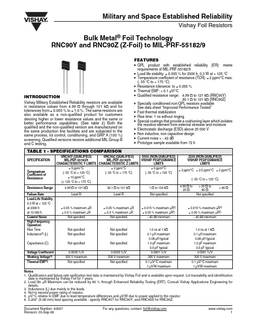
Document Number: 63007For any questions, contact: foil@Military and Space Established ReliabilityVishay Foil ResistorsBulk Metal ® Foil TechnologyRNC90Y and RNC90Z (Z-Foil) to MIL-PRF-55182/9INTRODUCTIONVishay Military Established Reliability resistors are available in resistance values from 4.99 Ω through 121 k Ω and for tolerances from ± 0.005 % to ± 1.0 %. The same resistors are also available as a non-qualified product for customers desiring higher or lower resistance values and the same or better performance capabilities. (See table 2) Both the qualified and the non-qualified version are manufactured on the same production line facilities and are subjected to the same process, lot control, conditioning, and GRP A (100 %)screening. Qualified versions receive additional MIL Group B and C testing.FEATURES•QPL product with established reliability (R): meets requirements of MIL-PRF-55182/9•Load life stability: ± 0.005 % for 2000 h, 0.3 W at + 125 °C •Temperature coefficient of resistance (TCR): ± 2 ppm/°C max.(- 55 °C to + 175 °C)•Resistance tolerance: to ± 0.005 %•Thermal EMF: < 0.1 µV/°C•Qualified resistance range: 4.99 Ω to 121 k Ω (RNC90Y)30.1 Ω to 121 k Ω (RNC90Z)•Specially conditioned non-QPL resistors available See data sheet “Improved Performance Tested”•Fast thermal stabilization•Rise time: 1 ns without ringing•Special coatings that provide a cushioning layer which isolates the resistive element from external stresses and moisture •Electrostatic discharge (ESD) above 25 000 V •Non inductive, non capacitive design •Current noise < - 42 dB•Prototype sample available from 72 hNotes1.Qualification and failure rate verification test data is maintained by Vishay Foil and is available upon request. Lot traceability and identification data is maintained by Vishay Foil for 7 years.2.Load life ΔR Maximum can be reduced by 80 % through Enhanced Reliability Testing (ERT). Consult Vishay Applications Engineering for details.3.Inductance (L) due mainly to the leads.4.Not to exceed power rating of resistor.5.µV/°C relates to EMF due to lead temperature differences and µV/W due to power applied to the resistor.6.0.200" (5.08 mm) lead spacing available - specify RNC90T for RNC90Y, and RNC90S for RNC90Z.TABLE 1 - SPECIFICATIONS COMPARISONSPECIFICATION RNC90Y (QUALIFIED) MIL-PRF-55182/9 CHARACTERISTIC Y LIMITS RNC90Z (QUALIFIED) MIL-PRF-55182/9 CHARACTERISTIC Z LIMITS S555 (NON-QUALIFIED)VISHAY PERFORMANCE LIMITS Z555 (NON-QUALIFIED)VISHAY PERFORMANCE LIMITSTemperature Coefficient of Resistance ± 5 ppm/°C ± 2 ppm/°C ± 5 ppm/°C± 3 ppm/°C ± 2.5 ppm/°C ± 2 ppm/°C(- 55 °C to + 125 °C)(- 55 °C to + 175 °C)(- 55 °C to + 125 °C)± 10 ppm/°C(- 55 °C to + 125 °C)(+ 125 °C to + 175 °C)Resistance Range 4.99 Ω to 121 k Ω30.1 Ω to 121 k Ω 1 Ω to 150 k Ω 4.99 Ω to 25 Ω> 25 Ω to 80 Ω> 80 ΩFailure RateLevel R Level R Not specified Not specifiedLoad-Life Stability 0.3 W at + 125 °C at 2000 h ± 0.05 % maximum ΔR ± 0.05 % maximum ΔR ± 0.015 % maximum ΔR 2)± 0.015 % maximum ΔR 2)at 10000 h ± 0.5 % maximum ΔR± 0.5 % maximum ΔR± 0.05 % maximum ΔR 2)± 0.05 % maximum ΔR 2)Current Noise Not specified Not specified - 40 dB minimum - 40 dB minimumHigh-Frequency Operation Rise TimeNot specified Not specified 1.0 ns at 1 k Ω 1.0 ns at 1 k ΩInductance 3) (L)Not specified Not specified 0.1 µH maximum 0.1 µH maximum 0.08 µH typical 0.08 µH typical Capacitance (C)Not specified Not specified 1.0 pF maximum 1.0 pF maximum 0.5 pF typical 0.5 pF typical Voltage Coefficient 0.0005 %/V 0.0005 %/V 0.0001 %/V 0.0001 %/V Working Voltage 4)300 V maximum 300 V maximum 300 V maximum 300 V maximum Thermal EMF 5)Not specifiedNot specified0.1 µV/°C maximum 0.1 µV/°C maximum 1 µV/W maximum 1 µV/W maximumMilitary and Space Established ReliabilityVishay Foil ResistorsBulk Metal ® Foil TechnologyRNC90Y and RNC90Z (Z-Foil) to MIL-PRF-55182/9 For any questions, contact: foil@Document Number: 63007Document Number: 63007For any questions, contact: foil@Military and Space Established ReliabilityBulk Metal ® Foil Technology RNC90Y and RNC90Z (Z-Foil) to MIL-PRF-55182/9Vishay Foil ResistorsNote•S555 and Z555 units are manufactured on the same production line facilities and are subjected to all the same process and lot control requirements imposed on RNC90Y (Z) version, as well as all of the special screening, environmental conditioning and documentation stipulations outlined in MIL-PRF 55182/9Note* For non-standard requests, please contact application engineering.TABLE 2 - MODEL SELECTIONMODELNUMBER RESISTANCE RANGE (Ω)STANDARD RESISTANCETOLERANCE FAILURE RATE AMBIENT POWER RATING AVERAGE WEIGHT(g)DIMENSIONS TIGHTEST %LOOSEST %at + 70 °C at + 125 ° C INCHES mmRNC90Y30.1 to 121K ± 0.005± 1.0M, P , R (SeeT able 3)0.6 W 0.3 W 0.6W: 0.105 ± 0.010L: 0.300 ± 0.010H: 0.326 ± 0.010ST: 0.015 ± 0.005SW: 0.040 ± 0.005LL: 1.000 ± 0.125LS: 0.150 ± 0.005 2.67 ± 0.257.62 ± 0.258.28 ± 0.250.38 ± 0.131.02 ± 0.1325.4 ± 3.183.81 ± 0.1316.2 to 30.0± 0.05± 1.04.99 to 16.0± 0.1± 1.0RNC90Z 30.1 to 121K ± 0.005± 1.00.6 W 0.3 W 0.6S555(NON QPL)30.1 to 121K ± 0.005± 1.0-0.6 W 0.3 W 0.620 to < 30.1± 0.01± 1.05 to < 20± 0.05± 1.02 to < 5± 0.1± 1.01 to < 2± 0.5± 1.0> 121K to 150K ± 0.005± 1.0-0.4 W 0.2 W 0.6Z555(NON QPL)30.1 to 121K ± 0.005± 1.0-0.6 W 0.3 W 0.620 to < 30.1± 0.01± 1.04.99 to < 20R ± 0.05± 1.0TABLE 3 - GLOBAL PART NUMBER INFORMATIONNEW GLOBAL PART NUMBER:Y1189100R500AR0L (preferred part number format)DENOTES PRECISIONVALUE LIFE FAILURE RATE (LFR)AER*YR = ΩK = k ΩR = ± 0.01 %P = ± 0.1 %M = ± 1.0 %0 = standard 1 - 999 = customPRODUCT CODE RESIST ANCE TOLERANCEPACKAGING 1189 = RNC90Z 0089 = RNC90Y 1508 = RNC90T 1506 = RNC90S 0088 = S5551288 = Z555V = ± 0.005 %T = ± 0.01 %A = ± 0.05 %B = ± 0.1 %D = ± 0.5 %F = ± 1.0 %L = bulk pack R = tape and reelFOR EXAMPLE: ABOVE GLOBAL ORDER Y1189 100R500 A R 0 L:TYPE: RNC90Z VALUE: 100.5 ΩABSOLUTE TOLERANCE: ± 0.05 %LIFE FAILURE RATE (LFR): ± 0.01 %AER: standardPACKAGING: bulk packHISTORICAL PART NUMBER:RNC90Z 100R50A R B (will continue to be used)RNC90Z 100R50A R B MODEL OHMIC VALUERESIST ANCE TOLERANCE LIFE FAILURE RA TE (LFR)P ACKAGING RNC90Z RNC90S RNC90Y RNC90T S555Z555100.5 ΩV = ± 0.005 %T = ± 0.01 %A = ± 0.05 %B = ± 0.1 %D = ± 0.5 %F = ± 1.0 %R = ± 0.01 %P = ± 0.1 %M = ± 1.0 %B = bulk pack18910R 50Y 1A R 000LMilitary and Space Established ReliabilityVishay Foil ResistorsBulk Metal ® Foil TechnologyRNC90Y and RNC90Z (Z-Foil) to MIL-PRF-55182/9 For any questions, contact: foil@Document Number: 63007The response of military and non military grade resistors to environmental stresses can be made better by “Improved Performance Testing” (IPT). The IPT part will see burn-in and cycling that removes the “knee” from the normal drift of non IPT parts. (See Table 4 for the improvement to expect in military parts when calling for Vishay recommended screening). Users should be aware that IPT testing renders the part non QPL and so a 3XXXXX part number will be assigned by Vishay. Consult Applications Engineering for details and ordering advice.CAGE #18612“Commercial and Government Entity”Formerly “FSCM”TABLE 4 - IMPROVED PERFORMANCE TESTING (NON-QPL APPROVED) VS. QPLTEST GROUPTESTRNC90YMIL-PRF-55182/9VISHAYIMPROVED PERFORMANCETESTING (IPT) LIMITS METHOD PARAGRAPHLIMITS IPower Conditioning not done -± 0.0025 %Thermal Shock and 4.8.2-± 0.0025 %Overload Combined 4.8.3± 0.05 %± 0.0025 %IIResistance TemperatureCharacteristic 4.8.9± 5 ppm/°C< ± 2 ppm/°C (- 55 °C to + 125 °C)(Can be sorted for tighter tracking)Low T emperature Storage 4.8.23± 0.05 %± 0.0025 %Low Temperature Operation4.8.10± 0.05 %± 0.0025 %T erminal Strength4.8.11± 0.02 %± 0.001 %IIIDWV4.8.12± 0.02 %± 0.001 %Insulation Resistance 4.8.13104 M Ω> 104 M ΩResistance to Soldering Heat4.8.14± 0.02 %± 0.001 %Moisture Resistance4.8.15± 0.05 %± 0.015 %IV Shock 4.8.16± 0.01 %± 0.0025 %Vibration4.8.17± 0.02 %± 0.0025 %V Load Life at + 125 °C; 2000 h 4.8.18± 0.05 %± 0.005 % (50 ppm)Load Life at + 125 °C; 10000 h4.8.18± 0.5 %± 0.015 % (150 ppm)V (a)+ 85 °C Power Rating --± 0.005 % (50 ppm)+ 70 °C Power Rating 4.8.18± 0.05 %± 0.005 % (50 ppm)V (b)+ 25 °C Power Rating--± 0.005 % (50 ppm)VI Storage Life--± 0.0025 %VII High T emperature Exposure 4.8.19± 0.5 %± 0.005 %VIIIMax. Allowance Reactance--< 1 %Current Noise --< - 42 dB Voltage Coefficient4.8.200.0005 %/V < 0.00001 %/V -(5 ppm/V)(< 0.1 ppm/V)Thermal EMF--0.1 µV/°CDisclaimer Legal Disclaimer NoticeVishayAll product specifications and data are subject to change without notice.Vishay Intertechnology, Inc., its affiliates, agents, and employees, and all persons acting on its or their behalf (collectively, “Vishay”), disclaim any and all liability for any errors, inaccuracies or incompleteness contained herein or in any other disclosure relating to any product.Vishay disclaims any and all liability arising out of the use or application of any product described herein or of any information provided herein to the maximum extent permitted by law. The product specifications do not expand or otherwise modify Vishay’s terms and conditions of purchase, including but not limited to the warranty expressed therein, which apply to these products.No license, express or implied, by estoppel or otherwise, to any intellectual property rights is granted by this document or by any conduct of Vishay.The products shown herein are not designed for use in medical, life-saving, or life-sustaining applications unless otherwise expressly indicated. Customers using or selling Vishay products not expressly indicated for use in such applications do so entirely at their own risk and agree to fully indemnify Vishay for any damages arising or resulting from such use or sale. Please contact authorized Vishay personnel to obtain written terms and conditions regarding products designed for such applications.Product names and markings noted herein may be trademarks of their respective owners.元器件交易网Document Number: 。
华测 X90 接收机 说明书

目录第1章X90RTK快速入门 (1)1.1X90接收机 (1)1.1.1卫星灯 (1)1.1.2数据采集灯 (1)1.1.3无线电指示灯 (2)1.1.4电源灯 (2)1.1.5切换键 (2)1.1.6串口和无线电接口 (2)1.2常规注意事项 (2)第2章华测RTK测量软件 (4)2.1RTK软件的安装与卸载 (4)2.1.1安装 (4)2.1.2卸载 (7)2.2手簿软件的安装与卸载 (10)2.2.1微软同步软件(ActiveSync)的安装 (10)2.2.2与电脑同步 (11)2.2.3测地通软件的安装 (12)第3章测地通软件 (15)3.1文件 (15)3.1.1新建任务 (15)3.1.2打开任务 (16)3.1.3保存任务 (16)3.1.4另存任务 (17)3.1.5任务属性 (17)3.1.6当前坐标参数 (18)3.1.7元素管理器 (20)3.1.7.1点管理器 (20)3.1.7.2直线管理器 (22)3.1.7.3点分类器 (23)3.1.8导入 (24)3.1.8.1当地点坐标导入 (24)3.1.8.284点坐标导入 (26)3.1.8.3直线导入 (26)3.1.8.4成果导入 (27)3.1.8.5导入/清空DXF文件 (27)3.1.8.6电力线数据导入 (28)3.1.9导出 (28)3.1.9.1点坐标导出 (29)3.1.9.2直线导出 (29)3.1.9.3成果导出 (30)3.1.9.4测量点成果导出 (31)3.1.9.5放样成果导出 (31)3.1.9.6直线放样点导出 (31)3.1.9.7校正成果导出 (32)3.1.9.8导出DXF/自动连线DXF文件 (32)3.1.9.9电力线数据导出 (32)3.1.9.10福建海洋数据导出 (33)3.1.9.11HTML测量点成果导出 (33)3.1.10退出 (33)3.2键入 (34)3.2.1键入点 (34)3.2.2键入直线 (35)3.3配置 (37)3.3.1移动站参数 (37)3.3.1.1移动站选项 (37)3.3.1.2内置电台和GPRS (38)3.3.1.3手簿网络 (40)3.3.1.4内置VRS移动站 (40)3.3.1.5手簿CORS (41)3.3.2基准站选项 (42)3.3.3坐标系管理 (43)3.3.4手簿端口配置 (43)3.3.5测深仪配置 (44)3.3.6测量点选项 (44)3.1.6.1地形点选项 (45)3.1.6.2观测控制点选项 (45)3.1.6.3快速点选项 (46)3.1.6.4连续点选项 (46)3.3.7放样格式 (47)3.3.8设置GPS类型 (47)3.3.9语言选择 (48)3.3.10软件注册 (48)3.3.11天线管理 (49)3.4测量 (50)3.4.1启动基准站接收机 (50)3.4.2启动移动站接收机 (51)3.4.3测量点 (53)3.4.4连续地形 (53)3.4.5其它测量 (54)3.4.6点放样 (55)3.4.6.1常规点放样 (55)3.4.6.2分类器放样 (58)3.4.7线放样 (59)3.4.7.1直线放样 (59)3.4.7.2直线库放样 (61)3.4.8道路放样 (62)3.4.9其他放样 (63)3.4.9.1轨迹放样 (63)3.4.9.3参考线放样 (64)3.4.9.4地震线放样 (65)3.4.9.5石油物探 (66)3.4.10点校正 (66)3.5坐标计算 (67)3.5.1反算计算 (67)3.5.2计算点 (68)3.5.3计算道路点 (69)3.5.4面积周长计算 (70)3.5.5计算方位角 (70)3.5.6计算偏转角 (71)3.5.7计算距离 (72)3.5.8划分线 (73)3.5.9计算器 (73)3.6仪器 (74)3.6.1星空图 (74)3.6.2卫星状态 (75)3.6.3位置 (75)3.6.4点位图 (76)3.6.5导航到基准站 (77)3.6.6接收机状态 (78)3.6.7接收机设置 (78)3.6.8接收机选项 (79)3.6.9接收机复位 (80)3.6.10超级终端 (80)3.6.11软件版本 (81)第4章道路放样测量 (83)4.1道路放样简介 (83)4.2道路放样测量 (83)4.2.1PC版道路编辑软件使用方法 (84)4.2.2手簿软件使用方法 (91)第5章测地通软件在电力线测量中的应用 (104)5.1电力线测量简介 (104)5.2电力线选线 (104)5.3电力线测量 (106)5.3.1直线放样方法 (106)5.3.2电力线放样方法 (106)5.3.2.1转角测量 (107)5.3.2.2碎步点测量 (107)5.3.2.3直线桩测量 (108)5.3.2.4房屋测量 (108)5.3.2.5跨越测量 (109)5.3.2.6沟、河测量 (110)5.3.2.7道路测量 (111)5.3.2.8池塘测量 (112)5.3.2.9坟的测量 (113)5.3.2.10断面测量 (113)5.3.2.11小结 (114)5.4数据导出 (114)5.4.1直线放样方法测量电力线数据导出 (114)5.4.2电力线放样方法数据导出 (115)5.5转换为道亨数据格式 (116)5.5.1直线放样数据转换 (116)5.5.2电力线放样数据转换 (118)5.6道亨软件点号的编码规则 (118)5.6.1点名的命名规则 (118)5.6.2房子的命名规则 (119)5.6.3跨越的命名方法 (119)5.6.4沟、河的命名方法 (120)5.6.5路的命名 (120)5.6.6塘的命名规则 (121)5.6.7坟的命名规则 (122)5.6.8断面连线 (122)第6章附录 (123)简介本章介绍的X90接收机是专门为GPS测量应用而设计的仪器,具有单触式记录的特点,操作简便。
STW9NK90Z中文资料

1/11April 2003STP9NK90Z -STF9NK90ZSTW9NK90ZN-CHANNEL 900V -1.1Ω-8A TO-220/TO-220FP/TO-247Zener-Protected SuperMESH™Power MOSFETs TYPICAL R DS (on)=1.1Ωs EXTREMELY HIGH dv/dt CAPABILITY s 100%AVALANCHE TESTED s GATE CHARGE MINIMIZEDs VERY LOW INTRINSIC CAPACITANCES sVERY GOOD MANUFACTURING REPEATIBILITYDESCRIPTIONThe SuperMESH™series is obtained through an extreme optimization of ST’s well established strip-based PowerMESH™layout.In addition to pushing on-resistance significantly down,special care is tak-en to ensure a very good dv/dt capability for the most demanding applications.Such series comple-ments ST full range of high voltage MOSFET s in-cluding revolutionary MDmesh™products.APPLICATIONSs HIGH CURRENT,HIGH SPEED SWITCHING s SWITCH MODE POWER SUPPLIESs DC-AC CONVERTERS FOR WELDING,UPS AND MOTOR DRIVEORDERING INFORMATIONTYPE V DSS R DS(on)I D Pw STP9NK90Z STF9NK90Z STW9NK90Z900V 900V 900V<1.3Ω<1.3Ω<1.3Ω8A 8A 8A160W 40W 160WSALES TYPE MARKING PACKAGE PACKAGINGSTP9NK90Z P9NK90Z TO-220TUBE STF9NK90Z F9NK90Z TO-220FP TUBE STW9NK90ZW9NK90ZTO-247TUBESTP9NK90Z -STF9NK90Z -STW9NK90Z2/11ABSOLUTE MAXIMUM RATINGS( )Pulse width limited by safe operating area(1)I SD ≤8A,di/dt ≤200A/µs,V DD ≤V (BR)DSS ,T j ≤T JMAX.(*)Limited only by maximum temperature allowedTHERMAL DATAAVALANCHE CHARACTERISTICSGATE-SOURCE ZENER DIODEPROTECTION FEATURES OF GATE-TO-SOURCE ZENER DIODESThe built-in back-to-back Zener diodes have specifically been designed to enhance not only the device’s ESD capability,but also to make them safely absorb possible voltage transients that may occasionally be applied from gate to source.In this respect the Zener voltage is appropriate to achieve an efficient and cost-effective intervention to protect the device’s integrity.These integrated Zener diodes thus avoid the usage of external components.Symbol ParameterValueUnit STP9NK90ZSTF9NK90ZSTW9NK90ZV DS Drain-source Voltage (V GS =0)900V V DGR Drain-gate Voltage (R GS =20k Ω)900V V GS Gate-source Voltage±30VI D Drain Current (continuous)at T C =25°C 88(*)8A I D Drain Current (continuous)at T C =100°C 55(*)5A I DM ( )Drain Current (pulsed)3232(*)32A P TOT Total Dissipation at T C =25°C 16040160W Derating Factor1.280.32 1.28W/°C V ESD(G-S)Gate source ESD(HBM-C=100pF,R=1.5K Ω)4KV dv/dt (1)Peak Diode Recovery voltage slope 4.5V/nsV ISO Insulation Withstand Voltage (DC)-2500-V T j T stgOperating Junction Temperature Storage Temperature-55to 150-55to 150°C °CTO-220TO-220FPTO-247Rthj-case Thermal Resistance Junction-case Max 0.783.10.78°C/W Rthj-ambThermal Resistance Junction-ambient Max62.550°C/W T lMaximum Lead Temperature For Soldering Purpose300°CSymbol ParameterMax ValueUnit I AR Avalanche Current,Repetitive or Not-Repetitive (pulse width limited by T j max)8A E ASSingle Pulse Avalanche Energy(starting T j =25°C,I D =I AR ,V DD =50V)300mJSymbol ParameterTest ConditionsMin.Typ.Max.Unit BV GSOGate-Source Breakdown VoltageIgs=±1mA (Open Drain)30V3/11STP9NK90Z -STF9NK90Z -STW9NK90ZELECTRICAL CHARACTERISTICS (T CASE =25°C UNLESS OTHERWISE SPECIFIED)ON/OFFDYNAMICSWITCHING ONSWITCHING OFFSOURCE DRAIN DIODENote: 1.Pulsed:Pulse duration =300µs,duty cycle 1.5%.2.Pulse width limited by safe operating area.3.C oss eq.is defined as a constant equivalent capacitance giving the same charging time as C oss when V DS increases from 0to 80%V DSS .Symbol ParameterTest ConditionsMin.Typ.Max.Unit V (BR)DSS Drain-sourceBreakdown Voltage I D =1mA,V GS =0900V I DSS Zero Gate VoltageDrain Current (V GS =0)V DS =Max RatingV DS =Max Rating,T C =125°C 150µA µA I GSS Gate-body Leakage Current (V DS =0)V GS =±20V±10µA V GS(th)Gate Threshold Voltage V DS =V GS ,I D =100µA 33.754.5V R DS(on)Static Drain-source On ResistanceV GS =10V,I D =3.6A1.11.3ΩSymbol ParameterTest ConditionsMin.Typ.Max.Unit g fs (1)Forward Transconductance V DS =15V ,I D =3.6A5.75S C iss C oss C rss Input Capacitance Output Capacitance Reverse Transfer Capacitance V DS =25V,f =1MHz,V GS =0211519040pF pF pF C oss eq.(3)Equivalent Output CapacitanceV GS =0V,V DS =0V to 720V115pFSymbol ParameterTest ConditionsMin.Typ.Max.Unit t d(on)t r Turn-on Delay Time Rise TimeV DD =450V,I D =4A R G =4.7ΩV GS =10V(Resistive Load see,Figure 3)2213ns ns Q g Q gs Q gdTotal Gate Charge Gate-Source Charge Gate-Drain ChargeV DD =720V,I D =8A,V GS =10V721438100nC nC nCSymbol ParameterTest ConditionsMin.Typ.Max.Unit t d(off)t f Turn-off Delay Time Fall TimeV DD =450V,I D =4A R G =4.7ΩV GS =10V(Resistive Load see,Figure 3)5528ns ns t r(Voff)t f t cOff-voltage Rise Time Fall TimeCross-over TimeV DD =720V,I D =8A,R G =4.7Ω,V GS =10V(Inductive Load see,Figure 5)531122ns ns nsSymbol ParameterTest ConditionsMin.Typ.Max.Unit I SD I SDM (2)Source-drain CurrentSource-drain Current (pulsed)832A A V SD (1)Forward On Voltage I SD =8A,V GS =0 1.6V t rr Q rr I RRMReverse Recovery Time Reverse Recovery Charge Reverse Recovery CurrentI SD =8A,di/dt =100A/µs V DD =50V,T j =150°C (see test circuit,Figure 5)9501021ns µC ASTP9NK90Z -STF9NK90Z -STW9NK90Z4/11Safe Operating Area For TO-2475/11STP9NK90Z -STF9NK90Z -STW9NK90ZStatic Drain-source On ResistanceTransferCharacteristicsTransconductanceSTP9NK90Z -STF9NK90Z -STW9NK90Z6/11Normalized BVDSS vs TemperatureSource-drain Diode Forward Characteristics7/11STP9NK90Z -STF9NK90Z -STW9NK90ZFig.5:Test Circuit For Inductive Load Switching And Diode Recovery TimesFig.4:Gate Charge test CircuitFig.2:Unclamped Inductive WaveformFig.1:Unclamped Inductive Load TestCircuitFig.3:Switching Times Test Circuit For ResistiveLoadSTP9NK90Z-STF9NK90Z-STW9NK90Z8/11STP9NK90Z-STF9NK90Z-STW9NK90Z9/11STP9NK90Z-STF9NK90Z-STW9NK90Z10/11元器件交易网STP9NK90Z-STF9NK90Z-STW9NK90Z Information furnished is believed to be accurate and reliable. However, STMicroelectronics assumes no responsibility for theconsequences of use of such information nor for any infringement of patents or other rights of third parties which may result fromits use. No license is granted by implication or otherwise under any patent or patent rights of STMicroelectronics. Specificationsmentioned in this publication are subject to change without notice. This publication supersedes and replaces all informationpreviously supplied. STMicroelectronics products are not authorized for use as critical components in life support devices orsystems without express written approval of STMicroelectronics.© The ST logo is a registered trademark of STMicroelectronics© 2003 STMicroelectronics - Printed in Italy - All Rights ReservedSTMicroelectronics GROUP OF COMPANIESAustralia - Brazil - Canada - China - Finland - France - Germany - Hong Kong - India - Israel - Italy - Japan - Malaysia - Malta - MoroccoSingapore - Spain - Sweden - Switzerland - United Kingdom - United States.© 11/11。
RNC各接口集成手册共43页word资料

目录1NOKIA的RNC简介 (2)2 RNC Iu-cs接口集成步骤及所需注意事项 (8)2.1 创建物理端口 (8)2.2 创建ATM层 (8)2.3 创建控制平面的MTP层 (9)2.4 创建控制平面的SCCP层配置 (12)2.5 创建用户平面 (14)3 RNC Iu-ps接口集成步骤及所需注意事项 (17)3.1 建物理端口 (17)3.2 创建ATM层 (17)3.3 创建控制平面的MTP层 (19)3.4 创建控制平面的SCCP层配置 (20)3.5 建用户平面 (22)4 RNC Iur接口集成步骤及所需注意事项 (25)4.1 创建ATM资源 (25)4.2 创建控制面数据 (25)4.3创建用户平面 (28)5RNC Iub接口集成步骤及所需注意事项 (30)5.1 创建IMA 组 (30)5.2 创建物理端口 (30)5.3 创建ATM层 (30)5.4 下面在NOKIA图形界面中创建VP,VC及其一些基站参数 (31)RNC无线网络控制器定义无线网络控制器(RNC,Radio Network Controller)是新兴3G网络的一个关键网元。
它是接入网的组成部分,用于提供移动性管理、呼叫处理、链接管理和切换机制。
为了实现这些功能,RNC必须利用出色的可靠性和可预测的性能,以线速执行一整套复杂且要求苛刻协的议处理任务。
作为3G 网络的重要组成部分,无线网络控制器(RNC)是流量汇集、转换、软硬呼叫转移(soft and hard call handoffs)、及智能小区和分组处理的重点。
无线网络控制器(RNC)的高级任务包括1) 管理用于传输用户数据的无线接入载波;2) 管理和优化无线网络资源;3) 移动性控制;和4) 无线链路维护。
无线网络控制器(RNC)具有组帧分配(framing distribution)与选择、加密、解密、错误检查、监视、以及状态查询等功能。
无线网络控制器(RNC)还可提供桥接功能,用于连接IP分组交换网络。
W12NK90Z中文资料

W12NK90Z中⽂资料October 2006 Rev 51/14STW12NK90ZN-channel 900V - 0.72? - 11A - TO-247Zener-protected SuperMESH? Power MOSFETGeneral features■Extremely high dv/dt capability ■100% avalanche tested ■Gate charge minimized ■Very low intrinsic capacitances ■Very good manufacturing repeatibilityDescriptionThe SuperMESH? series is obtained through an extreme optimization of ST’s well established strip-based PowerMESH? layout. In addition to pushing on-resistance significantly down, special care is taken to ensure a very good dv/dtcapability for the most demanding applications. Such series complements ST full range of high voltage MOSFETs including revolutionary MDmesh? products.Applications■Switching applicationType V DSS R DS(on)I D p W STW12NK90Z900V<0.88?11A230W/doc/a62e0e2c58fb770bf78a556d.htmlOrder codesPart number Marking Package Packaging STW12NK90ZW12NK90ZTO-247T ubeContents STW12NK90ZContents1Electrical ratings . . . . . . . . . . . . . . . . . . . . . . . . . . . . . . . . . . . . . . . . . . . . 31.1Protection features of gate-to-source zener diodes . . . . . . . . . . . . . . . . . . 42Electrical characteristics . . . . . . . . . . . . . . . . . . . . . . . . . . . . . . . . . . . . . 52.1Electrical characteristics (curves) . . . . . . . . . . . . . . . . . . . . . . . . . . . . . 7 3Test circuit . . . . . . . . . . . . . . . . . . . . . . . . . . . . . . . . . . . . . . . . . . . . . . . . 9 4Package mechanical data . . . . . . . . . . . . . . . . . . . . . . . . . . . . . . . . . . . . 11 5Revision history . . . . . . . . . . . . . . . . .. . . . . . . . . . . . . . . . . . . . . . . . . . 132/14STW12NK90Z Electrical ratings3/141 Electrical ratingsTable 1.Absolute maximum ratingsSymbol ParameterValue Unit V DS Drain-source voltage (V GS = 0)900V V GS Gate- source voltage± 30V I D Drain current (continuous) at T C = 25°C 11A I D Drain current (continuous) at T C = 100°C 7A I DM (1)1.Pulse width limited by safe operating area.Drain current (pulsed)44A P totT otal dissipation at T C = 25°C 230W Derating Factor1.85W/°C V ESD(G-S)Gate source ESD(HBM-C=100pF , R=1.5K ?)6000V E AS (2)2. I SD ≤11A, di/dt ≤200A/µs, V DD ≤ V (BR)DSS , T j ≤ T JMAX.Single pulse avalanche energy 4.5mJ T stg Storage temperature-55 to 150°CT jMax. operating junction temperatureTable 2.Thermal dataRthj-case Thermal resistance junction-case max 0.54°C/W Rthj-ambThermal resistance junction-ambient max 50°C/W T JMaximum lead temperature for soldering purpose300°CTable 3.Avalanche characteristicsSymbol ParameterMax valueUnit I AR Avalanche current, repetitive or not-repetitive(pulse width limited by T j max)11A E ASSingle pulse avalanche energy(starting T j = 25 °C, I D = I AR , V DD = 50 V)500mJTable 4.Gate-source zener diodeSymbol ParameterTest conditions Min.Typ.Max.Unit BV GSOGate-source breakdown voltageIgs=± 1mA (open drain)30VElectrical ratings STW12NK90Z1.1 Protection features of gate-to-source zener diodesThe built-in back-to-back Zener diodes have specifically been designed to enhance not onlythe device’s ESD capability, but also to make them safely absorb possible voltage transientsthat may occasionally be applied from gate to source. In this respect the Zener voltage isappropriate to achieve an efficient and cost-effective intervention to protect the device’sintegrity. These integrated Zener diodes thus avoid the usage of external components.4/14STW12NK90Z Electrical characteristics5/142 Electrical characteristics(T CASE =25°C unless otherwise specified)Table 5.On/off statesSymbol ParameterTest conditions Min.Typ.Max.Unit V (BR)DSSDrain-sourcebreakdown voltage I D = 1mA, V GS =0900V I DSSZero gate voltage drain current (V GS = 0)V DS = max rating V DS = max rating, T C = 125°C 150µA µA I GSS Gate-body leakage current (V DS = 0)V GS = ± 20V±10µA V GS(th)Gate threshold voltage V DS = V GS , I D = 100µA 33.754.5V R DS(on)Static drain-source on resistanceV GS = 10V , I D = 5.5A0.720.88Table 6.DynamicSymbol ParameterTest conditions Min.Typ.Max.Unit g fs (1)1.Pulsed: Pulse duration = 300 µs, duty cycle 1.5 %.Forwardtransconductance V DS = 15V , I D =5.5A11S C iss C oss C rss Input capacitance Output capacitance Reverse transfer capacitance V DS = 25V , f = 1MHz, V GS = 0 350028058pF pF pF C oss eq (2)2.Coss eq. is defined as a constant equivalent capacitance giving the same charging time as C oss when V DSincreases from 0 to 80% V DSS .Equivalent output capacitance V GS = 0V , V DS = 0V to 800V117pF t d(on)t r t d(off)t f Turn-on delay time Rise timeTurn-off delay time Fall timeV DD = 450V , I D = 5A R G =4.7? V GS = 10V (see Figure 13)31208855ns ns ns ns Q g Q gs Q gdTotal gate charge Gate-source charge Gate-drain chargeV DD = 720V , I D = 10A,V GS = 10V , R G =4.7?(see Figure 14)1131960152nC nC nCElectrical characteristics STW12NK90Z6/14Table 7.Source drain diodeSymbol Parameter Test conditions Min.Typ.Max.UnitI SDI SDM(1)1.Pulse width limited by safe operating area.Source-drain currentSource-drain current(pulsed)1144AA V SD(2)2.Pulsed: Pulse duration = 300 µs, duty cycle 1.5 % Forward on voltage I SD = 11A, V GS = 0 1.6V t rr Q rrI RRMReverse recovery timeReverse recovery chargeReverse recovery currentI SD = 10A, di/dt = 100A/µs,V DD = 50V, T j = 25°C(see Figure15)7287.821.6nsµCA t rrQ rrI RRMReverse recovery timeReverse recovery chargeReverse recovery currentI SD = 10A, di/dt = 100A/µs,V DD = 50V, T j = 150°C(see Figure15)9641123nsµCASTW12NK90Z Electrical characteristics7/142.1 Electrical characteristics (curves) Figure 1.Safe operating area Figure 2.Thermal impedanceFigure 3.Output characterisics Figure 4.Transfer characteristicsFigure 5.Transconductance Figure 6.Static drain-source on resistance Electrical characteristics STW12NK90Z8/14Figure 7.Gate charge vs gate-source voltage Figure 8. Capacitance variationsFigure 9.Normalized gate threshold voltageFigure 10.Normalized on resistance vs Figure 11.Source-drain diode forward Figure 12.Normalized breakdown voltage vs STW12NK90Z Test circuit9/143 Test circuitFigure 13.Switching times test circuit for Figure 14.Gate charge test circuitFigure 15.Test circuit for inductive load Figure 16.Unclamped Inductive load test Test circuitSTW12NK90Z10/14Figure 17.Unclamped inductive waveformFigure 18.Switching time waveformSTW12NK90Z Package mechanical data 4 Package mechanical dataIn order to meet environmental requirements, ST offers these devices in ECOPACK?packages. These packages have a Lead-free second level interconnect . The category ofsecond level interconnect is marked on the package and on the inner box label, incompliance with JEDEC Standard JESD97. The maximum ratings related to solderingconditions are also marked on the inner box label. ECOPACK is an ST trademark.ECOPACK specifications are available at: /doc/a62e0e2c58fb770bf78a556d.html11/14Package mechanical data STW12NK90Z12/14STW12NK90Z Revision history13/145 Revision historyTable 8.Revision historyDate RevisionChanges21-Jun-20044Complete version17-Oct-20065New template, no content changeSTW12NK90Z14/14Please Read Carefully:Information in this document is provided solely in connection with ST products. STMicroelectronics NV and its subsidiaries (“ST”) reserve the right to make changes, corrections, modifications or improvements, to this document, and the products and services described herein at any time, without notice.All ST products are sold pursuant to ST’s terms and conditions of sale.Purchasers are solely responsible for the choice, selection and use of the ST products and services described herein, and ST assumes no liability whatsoever relating to the choice, selection or use of the ST products and services described herein. No license, express or implied, by estoppel or otherwise, to any intellectual property rights is granted under this document. Ifany part of this document refers to any third party products or services it shall not be deemed a license grant by ST for the use of such third party products or services, or any intellectual property contained therein or considered as a warranty covering the use in any manner whatsoever of such third party products or services or any intellectual property contained therein. UNL ESS OTHERWISE SET FORTH IN ST’S TERMS AND CONDITIONS OF SAL E ST DISCL AIMS ANY EXPRESS OR IMPL IED WARRANTY WITH RESPECT TO THE USE AND/OR SAL E OF ST PRODUCTS INCL UDING WITHOUT L IMITATION IMPL IED WARRANTIES OF MERCHANTABILITY, FITNESS FOR A PARTICULAR PURPOSE (AND THEIR EQUIVALENTS UNDER THE LAWS OF ANY JURISDICTION), OR INFRINGEMENT OF ANY PATENT, COPYRIGHT OR OTHER INTELLECTUAL PROPERTY RIGHT. UNL ESS EXPRESSL Y APPROVED IN WRITING BY AN AUTHORIZED ST REPRESENTATIVE, ST PRODUCTS ARE NOT RECOMMENDED, AUTHORIZED OR WARRANTED FOR USE IN MILITARY, AIR CRAFT, SPACE, LIFE SAVING, OR LIFE SUSTAINING APPLICATIONS, NOR IN PRODUCTS OR SYSTEMS WHERE FAILURE OR MALFUNCTION MAY RESULT IN PERSONAL INJURY, DEATH, OR SEVERE PROPERTY OR ENVIRONMENTAL DAMAGE. ST PRODUCTS WHICH ARE NOT SPECIFIED AS "AUTOMOTIVE GRADE" MAY ONLY BE USED IN AUTOMOTIVE APPLICATIONS AT USER’S OWN RISK.Resale of ST products with provisions different from the statements and/or technical features set forth in this document shall immediately void any warranty granted by ST for the ST product or service described herein and shall not create or extend in any manner whatsoever, any liability of ST.ST and the ST logo are trademarks or registered trademarks of ST in various countries.Information in this document supersedes and replaces all information previously supplied.The ST logo is a registered trademark of STMicroelectronics. All other names are the property of their respective owners.2006 STMicroelectronics - All rights reservedSTMicroelectronics group of companiesAustralia - Belgium - Brazil - Canada - China - Czech Republic - Finland - France - Germany - Hong Kong - India - Israel -Italy - Japan - Malaysia - Malta - Morocco - Singapore - Spain - Sweden - Switzerland - United Kingdom - United States of America/doc/a62e0e2c58fb770bf78a556d.html。
Z90中文资料(rectron)中文数据手册「EasyDatasheet - 矽搜」

Z75 THRU Z330
DO-41
MA X IMU M R ATING S A ND E L E C T R IC A L C HA R A C T E R IS T IC S R a tings a t 25 C a mbie nt te mpe ra ture unle s s othe rwis e s pe cifie d. S ingle pha s e , ha lf wa ve , 6 0 H z , re s is tive or induc tive loa d. F or c a pa c itive loa d, de ra te c urre nt by 2 0 % .
5.0
150
5.0
160
5.0
170
5.0
180
5.0
200
5.0
220
5.0
240
5.0
Maximum Forward Voltage
@25 C T @I = 1.0A
V
V
1.2 1.2 1.2 1.2 1.2 1.2 1.2 1.2 1.2 1.2 1.2 1.2
2011-03 REV:B
芯片中文手册,看全文,戳
2500
.25
Z300300Fra bibliotek0.8
3000
.25
Z330
330
0.75
4000
.25
OPERATING AND STORAGE TEMPERATURE - 55 C to + 150 C
NOTE:1. Standard tolerance: +/-20%, Suffix “A” : +/-10% 2. “Fully ROHS compliant”, “100% Sn plating (Pb-free)”. 3. Available in Halogen-f ree epoxy by adding suf f ix -HF af ter the part nbr.
- 1、下载文档前请自行甄别文档内容的完整性,平台不提供额外的编辑、内容补充、找答案等附加服务。
- 2、"仅部分预览"的文档,不可在线预览部分如存在完整性等问题,可反馈申请退款(可完整预览的文档不适用该条件!)。
- 3、如文档侵犯您的权益,请联系客服反馈,我们会尽快为您处理(人工客服工作时间:9:00-18:30)。
Document Number: 63007For any questions, contact: foil@Military and Space Established ReliabilityVishay Foil ResistorsBulk Metal ® Foil TechnologyRNC90Y and RNC90Z (Z-Foil) to MIL-PRF-55182/9INTRODUCTIONVishay Military Established Reliability resistors are available in resistance values from 4.99 Ω through 121 k Ω and for tolerances from ± 0.005 % to ± 1.0 %. The same resistors are also available as a non-qualified product for customers desiring higher or lower resistance values and the same or better performance capabilities. (See table 2) Both the qualified and the non-qualified version are manufactured on the same production line facilities and are subjected to the same process, lot control, conditioning, and GRP A (100 %)screening. Qualified versions receive additional MIL Group B and C testing.FEATURES•QPL product with established reliability (R): meets requirements of MIL-PRF-55182/9•Load life stability: ± 0.005 % for 2000 h, 0.3 W at + 125 °C •Temperature coefficient of resistance (TCR): ± 2 ppm/°C max.(- 55 °C to + 175 °C)•Resistance tolerance: to ± 0.005 %•Thermal EMF: < 0.1 µV/°C•Qualified resistance range: 4.99 Ω to 121 k Ω (RNC90Y)30.1 Ω to 121 k Ω (RNC90Z)•Specially conditioned non-QPL resistors available See data sheet “Improved Performance Tested”•Fast thermal stabilization•Rise time: 1 ns without ringing•Special coatings that provide a cushioning layer which isolates the resistive element from external stresses and moisture •Electrostatic discharge (ESD) above 25 000 V •Non inductive, non capacitive design •Current noise < - 42 dB•Prototype sample available from 72 hNotes1.Qualification and failure rate verification test data is maintained by Vishay Foil and is available upon request. Lot traceability and identification data is maintained by Vishay Foil for 7 years.2.Load life ΔR Maximum can be reduced by 80 % through Enhanced Reliability Testing (ERT). Consult Vishay Applications Engineering for details.3.Inductance (L) due mainly to the leads.4.Not to exceed power rating of resistor.5.µV/°C relates to EMF due to lead temperature differences and µV/W due to power applied to the resistor.6.0.200" (5.08 mm) lead spacing available - specify RNC90T for RNC90Y, and RNC90S for RNC90Z.TABLE 1 - SPECIFICATIONS COMPARISONSPECIFICATION RNC90Y (QUALIFIED) MIL-PRF-55182/9 CHARACTERISTIC Y LIMITS RNC90Z (QUALIFIED) MIL-PRF-55182/9 CHARACTERISTIC Z LIMITS S555 (NON-QUALIFIED)VISHAY PERFORMANCE LIMITS Z555 (NON-QUALIFIED)VISHAY PERFORMANCE LIMITSTemperature Coefficient of Resistance ± 5 ppm/°C ± 2 ppm/°C ± 5 ppm/°C± 3 ppm/°C ± 2.5 ppm/°C ± 2 ppm/°C(- 55 °C to + 125 °C)(- 55 °C to + 175 °C)(- 55 °C to + 125 °C)± 10 ppm/°C(- 55 °C to + 125 °C)(+ 125 °C to + 175 °C)Resistance Range 4.99 Ω to 121 k Ω30.1 Ω to 121 k Ω 1 Ω to 150 k Ω 4.99 Ω to 25 Ω> 25 Ω to 80 Ω> 80 ΩFailure RateLevel R Level R Not specified Not specifiedLoad-Life Stability 0.3 W at + 125 °C at 2000 h ± 0.05 % maximum ΔR ± 0.05 % maximum ΔR ± 0.015 % maximum ΔR 2)± 0.015 % maximum ΔR 2)at 10000 h ± 0.5 % maximum ΔR± 0.5 % maximum ΔR± 0.05 % maximum ΔR 2)± 0.05 % maximum ΔR 2)Current Noise Not specified Not specified - 40 dB minimum - 40 dB minimumHigh-Frequency Operation Rise TimeNot specified Not specified 1.0 ns at 1 k Ω 1.0 ns at 1 k ΩInductance 3) (L)Not specified Not specified 0.1 µH maximum 0.1 µH maximum 0.08 µH typical 0.08 µH typical Capacitance (C)Not specified Not specified 1.0 pF maximum 1.0 pF maximum 0.5 pF typical 0.5 pF typical Voltage Coefficient 0.0005 %/V 0.0005 %/V 0.0001 %/V 0.0001 %/V Working Voltage 4)300 V maximum 300 V maximum 300 V maximum 300 V maximum Thermal EMF 5)Not specifiedNot specified0.1 µV/°C maximum 0.1 µV/°C maximum 1 µV/W maximum 1 µV/W maximumMilitary and Space Established ReliabilityVishay Foil ResistorsBulk Metal ® Foil TechnologyRNC90Y and RNC90Z (Z-Foil) to MIL-PRF-55182/9 For any questions, contact: foil@Document Number: 63007Document Number: 63007For any questions, contact: foil@Military and Space Established ReliabilityBulk Metal ® Foil Technology RNC90Y and RNC90Z (Z-Foil) to MIL-PRF-55182/9Vishay Foil ResistorsNote•S555 and Z555 units are manufactured on the same production line facilities and are subjected to all the same process and lot control requirements imposed on RNC90Y (Z) version, as well as all of the special screening, environmental conditioning and documentation stipulations outlined in MIL-PRF 55182/9Note* For non-standard requests, please contact application engineering.TABLE 2 - MODEL SELECTIONMODELNUMBER RESISTANCE RANGE (Ω)STANDARD RESISTANCETOLERANCE FAILURE RATE AMBIENT POWER RATING AVERAGE WEIGHT(g)DIMENSIONS TIGHTEST %LOOSEST %at + 70 °C at + 125 ° C INCHES mmRNC90Y30.1 to 121K ± 0.005± 1.0M, P , R (SeeT able 3)0.6 W 0.3 W 0.6W: 0.105 ± 0.010L: 0.300 ± 0.010H: 0.326 ± 0.010ST: 0.015 ± 0.005SW: 0.040 ± 0.005LL: 1.000 ± 0.125LS: 0.150 ± 0.005 2.67 ± 0.257.62 ± 0.258.28 ± 0.250.38 ± 0.131.02 ± 0.1325.4 ± 3.183.81 ± 0.1316.2 to 30.0± 0.05± 1.04.99 to 16.0± 0.1± 1.0RNC90Z 30.1 to 121K ± 0.005± 1.00.6 W 0.3 W 0.6S555(NON QPL)30.1 to 121K ± 0.005± 1.0-0.6 W 0.3 W 0.620 to < 30.1± 0.01± 1.05 to < 20± 0.05± 1.02 to < 5± 0.1± 1.01 to < 2± 0.5± 1.0> 121K to 150K ± 0.005± 1.0-0.4 W 0.2 W 0.6Z555(NON QPL)30.1 to 121K ± 0.005± 1.0-0.6 W 0.3 W 0.620 to < 30.1± 0.01± 1.04.99 to < 20R ± 0.05± 1.0TABLE 3 - GLOBAL PART NUMBER INFORMATIONNEW GLOBAL PART NUMBER:Y1189100R500AR0L (preferred part number format)DENOTES PRECISIONVALUE LIFE FAILURE RATE (LFR)AER*YR = ΩK = k ΩR = ± 0.01 %P = ± 0.1 %M = ± 1.0 %0 = standard 1 - 999 = customPRODUCT CODE RESIST ANCE TOLERANCEPACKAGING 1189 = RNC90Z 0089 = RNC90Y 1508 = RNC90T 1506 = RNC90S 0088 = S5551288 = Z555V = ± 0.005 %T = ± 0.01 %A = ± 0.05 %B = ± 0.1 %D = ± 0.5 %F = ± 1.0 %L = bulk pack R = tape and reelFOR EXAMPLE: ABOVE GLOBAL ORDER Y1189 100R500 A R 0 L:TYPE: RNC90Z VALUE: 100.5 ΩABSOLUTE TOLERANCE: ± 0.05 %LIFE FAILURE RATE (LFR): ± 0.01 %AER: standardPACKAGING: bulk packHISTORICAL PART NUMBER:RNC90Z 100R50A R B (will continue to be used)RNC90Z 100R50A R B MODEL OHMIC VALUERESIST ANCE TOLERANCE LIFE FAILURE RA TE (LFR)P ACKAGING RNC90Z RNC90S RNC90Y RNC90T S555Z555100.5 ΩV = ± 0.005 %T = ± 0.01 %A = ± 0.05 %B = ± 0.1 %D = ± 0.5 %F = ± 1.0 %R = ± 0.01 %P = ± 0.1 %M = ± 1.0 %B = bulk pack18910R 50Y 1A R 000LMilitary and Space Established ReliabilityVishay Foil ResistorsBulk Metal ® Foil TechnologyRNC90Y and RNC90Z (Z-Foil) to MIL-PRF-55182/9 For any questions, contact: foil@Document Number: 63007The response of military and non military grade resistors to environmental stresses can be made better by “Improved Performance Testing” (IPT). The IPT part will see burn-in and cycling that removes the “knee” from the normal drift of non IPT parts. (See Table 4 for the improvement to expect in military parts when calling for Vishay recommended screening). Users should be aware that IPT testing renders the part non QPL and so a 3XXXXX part number will be assigned by Vishay. Consult Applications Engineering for details and ordering advice.CAGE #18612“Commercial and Government Entity”Formerly “FSCM”TABLE 4 - IMPROVED PERFORMANCE TESTING (NON-QPL APPROVED) VS. QPLTEST GROUPTESTRNC90YMIL-PRF-55182/9VISHAYIMPROVED PERFORMANCETESTING (IPT) LIMITS METHOD PARAGRAPHLIMITS IPower Conditioning not done -± 0.0025 %Thermal Shock and 4.8.2-± 0.0025 %Overload Combined 4.8.3± 0.05 %± 0.0025 %IIResistance TemperatureCharacteristic 4.8.9± 5 ppm/°C< ± 2 ppm/°C (- 55 °C to + 125 °C)(Can be sorted for tighter tracking)Low T emperature Storage 4.8.23± 0.05 %± 0.0025 %Low Temperature Operation4.8.10± 0.05 %± 0.0025 %T erminal Strength4.8.11± 0.02 %± 0.001 %IIIDWV4.8.12± 0.02 %± 0.001 %Insulation Resistance 4.8.13104 M Ω> 104 M ΩResistance to Soldering Heat4.8.14± 0.02 %± 0.001 %Moisture Resistance4.8.15± 0.05 %± 0.015 %IV Shock 4.8.16± 0.01 %± 0.0025 %Vibration4.8.17± 0.02 %± 0.0025 %V Load Life at + 125 °C; 2000 h 4.8.18± 0.05 %± 0.005 % (50 ppm)Load Life at + 125 °C; 10000 h4.8.18± 0.5 %± 0.015 % (150 ppm)V (a)+ 85 °C Power Rating --± 0.005 % (50 ppm)+ 70 °C Power Rating 4.8.18± 0.05 %± 0.005 % (50 ppm)V (b)+ 25 °C Power Rating--± 0.005 % (50 ppm)VI Storage Life--± 0.0025 %VII High T emperature Exposure 4.8.19± 0.5 %± 0.005 %VIIIMax. Allowance Reactance--< 1 %Current Noise --< - 42 dB Voltage Coefficient4.8.200.0005 %/V < 0.00001 %/V -(5 ppm/V)(< 0.1 ppm/V)Thermal EMF--0.1 µV/°CDisclaimer Legal Disclaimer NoticeVishayAll product specifications and data are subject to change without notice.Vishay Intertechnology, Inc., its affiliates, agents, and employees, and all persons acting on its or their behalf (collectively, “Vishay”), disclaim any and all liability for any errors, inaccuracies or incompleteness contained herein or in any other disclosure relating to any product.Vishay disclaims any and all liability arising out of the use or application of any product described herein or of any information provided herein to the maximum extent permitted by law. The product specifications do not expand or otherwise modify Vishay’s terms and conditions of purchase, including but not limited to the warranty expressed therein, which apply to these products.No license, express or implied, by estoppel or otherwise, to any intellectual property rights is granted by this document or by any conduct of Vishay.The products shown herein are not designed for use in medical, life-saving, or life-sustaining applications unless otherwise expressly indicated. Customers using or selling Vishay products not expressly indicated for use in such applications do so entirely at their own risk and agree to fully indemnify Vishay for any damages arising or resulting from such use or sale. Please contact authorized Vishay personnel to obtain written terms and conditions regarding products designed for such applications.Product names and markings noted herein may be trademarks of their respective owners.元器件交易网Document Number: 。