2SC4420中文资料
CS22中文资料

32IXYS reserves the right to change limits, test conditions and dimensionsPhase Control ThyristorsElectrically Isolated Tab V RSM V RRM TypeV DSM V DRM V V 800 800CS 22-08io1M 12001200CS 22-12io1MSymbol ConditionsMaximum RatingsI T(AV)M T C = 85°C 180° sine ①16A T A = 25°C 180° sine ② 2.5A I TSMT VJ = 45°C t = 10 ms (50 Hz), sine 300A V R = 0 V t = 8.3 ms (60 Hz), sine 340A T VJ = T VJM t = 10 ms (50 Hz), sine 250A V R = 0 Vt = 8.3 ms (60 Hz), sine 285A I 2tT VJ = 45°C t = 10 ms (50 Hz), sine 450A 2s V R = 0 V t = 8.3 ms (60 Hz), sine 480A 2s T VJ = T VJM t = 10 ms (50 Hz), sine 300A 2s V R = 0 Vt = 8.3 ms (60 Hz), sine337A 2s (di/dt)crT VJ = T VJM repetitive, I T = 20 A 150A/µsf = 50Hz, t P = 200µs V D = 2/3 V DRM I G = 0.08 A non repetitive, I T = I T(AV)M 500A/µs di G /dt = 0.08 A/µs(dv/dt)cr T VJ = T VJM , V DR = 2/3 V DRM1000V/µs R GK = ∞, method 1 (linear voltage rise)P GM T VJ = T VJM t P = 30 µs 10W I T = I T(AV)Mt P = 300 µs5W P GAV 0.5W V RGM 10V T VJ -40...+150°C T VJM 150°C T stg -40...+125°C M dMounting torque M 3 or UNC 4-400.5-0.8Nm Weight3gFeatures•Thyristor for frequencies up to 400Hz •International standard package •Epoxy meets UL 94V-0•High performance glass passivated chip •Long-term stability of leakage current and blocking voltage•Plasitc overmolded tab for electrical isolation Applications•Motor control •Power converter •AC power controller•Light and temperature control•SCR for inrush current limiting in power supplies or AC drive Advantages•Space and weight savings •Simple mountingACGV RRM = 800-1200 V I T(AV)M = 16 AA = Anode, C = Cathode, G = Gate Tab = Isolated0 IsolatedA AC ① mounted on heatsink Data according to IEC 60747② without heatsink32IXYS reserves the right to change limits, test conditions and dimensionsSymbol ConditionsCharacteristic ValuesI R , I D T VJ = T VJM , V R = V RRM , V D = V DRM ≤5mA V T I T= 30 A, T VJ = 25°C≤1.5V V T0For power-loss calculations only (T VJ = 150°C)0.9V r T 18m ΩV GT V D = 6 V T VJ = 25°C ≤ 1.5V T VJ = -40°C ≤ 2.5V I GT V D = 6 VT VJ = 25°C ≤30mA T VJ = -40°C≤50mA V GD T VJ = T VJM , V D = 2/3 V DRM≤0.2V I GD ≤3mA I L T VJ = 25°C, t P = 10 µs≤100mA I G = 0.08 A, di G /dt = 0.08 A/µs I H T VJ = 25°C, V D = 6 V, R GK =∞≤80mA t gd T VJ = 25°C, V D = ½ V DRM≤2µs I G = 0.08 A, di G /dt = 0.08 A/µs R thJC DC current 2.5K/W R thCH DC current 0.5K/W R thJA DC current50K/W aMax. acceleration, 50 Hz50m/s 2Package Outline。
2SK1522中文资料(renesas)中文数据手册「EasyDatasheet - 矽搜」

7.如果这些产品或技术受日本出口管理限制,必须是 日本政府根据许可证出口,不能导入比批准目地以外国家.
禁止任何转移或再出口违反出口管制法律和日本及/或目地国家相关规定.
8.请与瑞萨科技公司对这些材料或产品进一步详情 其中所载.
芯片中文手册,看全文,戳
V GS = ±25 V, V DS = 0 V DS = 360 V, V GS = 0 V DS = 400 V, V GS = 0 ID =1毫安,V DS = 10 V ID = 25 A, V GS = 10 V * 1
ID = 25 A, V DS = 10 V * 1 VDS = 10 V, V GS = 0, F = 1兆赫
芯片中文手册,看全文,戳
2SK1521, 2SK1522
绝对最大额定值
(Ta = 25°C)
项目
漏极至源极电压
2SK1521
2SK1522
门源电压
漏极电流
漏电流峰值
身体流失二极管反向漏电流
频道耗散
通道温度
储存温度
注:1.PW
10 µs, 占空比
1%
2.价值在T C = 25°C
符号
ID = 25 A, V GS = 10 V, RL = 1.2
IF = 50 A, V GS = 0
IF = 50 A, V GS = 0, di F/ DT = 100 A /μs的
3
—
远期转移导纳
|yfs|
22
输入电容
Ciss —
输出电容
Coss —
反向传输电容
Crss —
导通延迟时间 上升时间 关断延迟时间 下降时间 身体向前漏二极管 电压
芯片datasheet---mic4420
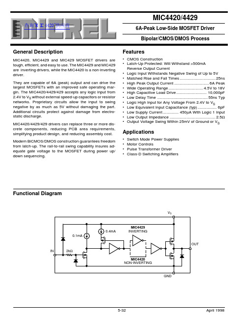
Electrical Characteristics: (T A = 25°C with 4.5V ≤ V S ≤ 18V unless otherwise specified.)Symbol ParameterConditionsMinTypMaxUnitsINPUT V IH Logic 1 Input Voltage 2.41.4V V IL Logic 0 Input Voltage 1.10.8V V IN Input Voltage Range –5V S + 0.3V I IN Input Current0 V ≤ V IN ≤ V S–1010µAOUTPUT V OH High Output Voltage See Figure 1V S –0.025V V OL Low Output Voltage See Figure 10.025V R O Output Resistance,I OUT = 10 mA, V S = 18 V 1.7 2.8ΩOutput Low R O Output Resistance,I OUT = 10 mA, V S = 18 V 1.5 2.5ΩOutput High I PK Peak Output Current V S = 18 V (See Figure 5)6A I RLatch-Up Protection>500mAWithstand Reverse CurrentSWITCHING TIME (Note 3)t R Rise Time Test Figure 1, C L = 2500 pF 1235ns t F Fall Time Test Figure 1, C L = 2500 pF 1335ns t D1Delay Time Test Figure 11875ns t D2Delay TimeTest Figure 14875nsPOWER SUPPLYI S Power Supply Current V IN = 3 V 0.45 1.5mA V IN = 0 V90150µA V SOperating Input Voltage4.518VAbsolute Maximum Ratings (Notes 1, 2 and 3)Supply Voltage (20V)Input Voltage...............................V S + 0.3V to GND – 5V Input Current (V IN > V S ).........................................50mA Power Dissipation, T A ≤ 25°CPDIP...................................................................960W SOIC .............................................................1040mW 5-Pin TO-220..........................................................2W Power Dissipation, T C ≤ 25°C5-Pin TO-220.....................................................12.5W Derating Factors (to Ambient)PDIP............................................................7.7mW/°C SOIC ...........................................................8.3mW/°C 5-Pin TO-220................................................17mW/°C Storage Temperature............................–65°C to +150°C Lead Temperature (10 sec.)..................................300°COperating RatingsJunction Temperature............................................150°C Ambient TemperatureC Version ................................................0°C to +70°C B Version.............................................–40°C to +85°C Package Thermal Resistance5-pin TO-220 (θJC )..........................................10°C/W 8-pin MSOP (θJA )..........................................250°C/W查询"MIC4420"供应商where:I H =quiescent current with input high I L =quiescent current with input lowD =fraction of time input is high (duty cycle)V S =power supply voltageTransition Power DissipationTransition power is dissipated in the driver each time its output changes state, because during the transition, for a very brief interval, both the N- and P-channel MOSFETs in the output totem-pole are ON simultaneously, and a current is conducted through them from V +S to ground. The transi-tion power dissipation is approximately:P T = 2 f V S (A•s)where (A•s) is a time-current factor derived from the typical characteristic curves.Total power (P D ) then, as previously described is:P D = P L + P Q +P TDefinitionsC L =Load Capacitance in Farads.D =Duty Cycle expressed as the fraction of time theinput to the driver is high.f =Operating Frequency of the driver in Hertz I H =Power supply current drawn by a driver whenboth inputs are high and neither output is loaded.I L =Power supply current drawn by a driver whenboth inputs are low and neither output is loaded.I D =Output current from a driver in Amps.P D =Total power dissipated in a driver in Watts.P L =Power dissipated in the driver due to the driver’sload in Watts.P Q =Power dissipated in a quiescent driver in Watts.P T =Power dissipated in a driver when the outputchanges states (“shoot-through current”) in Watts.NOTE: The “shoot-through” current from a dual transition (once up, once down) for both drivers is shown by the "Typical Characteristic Curve :Crossover Area vs. Supply Voltage and is in ampere-seconds. This figure must be multiplied by the number of repetitions per second (fre-quency) to find Watts.R O =Output resistance of a driver in Ohms.V S =Power supply voltage to the IC in Volts.Capacitive Load Power DissipationDissipation caused by a capacitive load is simply the energy placed in, or removed from, the load capacitance by the driver. The energy stored in a capacitor is described by the equation:E = 1/2 C V 2As this energy is lost in the driver each time the load is charged or discharged, for power dissipation calculations the 1/2 is removed. This equation also shows that it is good practice not to place more voltage on the capacitor than is necessary, as dissipation increases as the square of the voltage applied to the capacitor. For a driver with a capaci-tive load:P L = f C (V S )2where:f =Operating Frequency C =Load Capacitance V S =Driver Supply Voltage Inductive Load Power DissipationFor inductive loads the situation is more complicated. For the part of the cycle in which the driver is actively forcing current into the inductor, the situation is the same as it is in the resistive case:P L1 = I 2 R O DHowever, in this instance the R O required may be either the on resistance of the driver when its output is in the high state, or its on resistance when the driver is in the low state,depending on how the inductor is connected, and this is still only half the story. For the part of the cycle when the inductor is forcing current through the driver, dissipation is best described asP L2 = I V D (1-D)where V D is the forward drop of the clamp diode in the driver (generally around 0.7V). The two parts of the load dissipa-tion must be summed in to produce P LP L = P L1 + P L2Quiescent Power DissipationQuiescent power dissipation (P Q , as described in the input section) depends on whether the input is high or low. A low input will result in a maximum current drain (per driver) of ≤0.2mA; a logic high will result in a current drain of ≤2.0mA.Quiescent power can therefore be found from:P Q = V S [D I H + (1-D) I L ]查询"MIC4420"供应商。
2SC4250中文资料(toshiba)中文数据手册「EasyDatasheet - 矽搜」

反向传输电容 过渡频率 转换增益 噪声系数
(Ta = 25°C)
符号
测试条件
ICBO IEBO V (BR) CEO hFE Cre
fT Gce NF
VCB = 25 V, I E = 0 VEB = 3 V, I C = 0 IC = 1毫安,我B = 0 VCE = 10 V, I C = 5毫安 VCB = 10 V, I E = 0, f = 1兆赫 VCE = 10 V, I C = 5毫安 VCC = 12 V, f = 200兆赫,女 L = 260兆赫 (图1)
• 请联系您的东芝销售代表了解详细信息,以环境问题,如产品的RoHS指令的兼容性. 请遵守产品使用与规范纳入或使用受控物质,包括但不限于,欧盟RoHS指令的所有适用的法律和法规.东芝对发生违规作为适用的法律和法规而导致的损害 或损失不承担任何责任.
5
2007-11-01
• 东芝公司及其子公司和附属公司(统称为“TOSHIBA”),保留这份文件中更改信息的权利,以及相关的硬件,软件和系统(统称为“产品”),恕不另行通 知.
• 本文档以及任何信息均不得转载未经东芝事先书面许可.即使 东芝的书面许可,复制是允许的,只要在没有任何改动/遗漏.
• 虽然东芝的作品不断地提高产品的质量和可靠性,产品会发生故障或失败.客户 负责符合安全标准和用于提供充分的设计和保障其硬件,软件和 这最大限度地降低风险,并避免出现在产品的故障或失效可能导致生命丧失,身体系统 人身伤害或财产损失,包括数据丢失或损坏.在创作和制作的设计和使用,客户必须 也指,符合(一)中的所有相关信息,东芝的最新版本,包括但不限于本文件, 规格,数据表和应用笔记产品的注意事项和条件中规定的“TOSHIBA 半导体可靠性手册“和(b)对于该产品将与或使用的应用程序的说明.客户全权负责自己的产品设计或应用程序的各个方面,包括但不限于:(a)确定 的利用这样的设计或应用该产品的适当性; (b)评价和确定本文档中包含的任何信息的适用性,或图表,图表,程序,算法,示例应用电路,或 任何其他引用文件; (三)验证这样的设计和应用的所有运行参数.
442SA2TADN中文资料
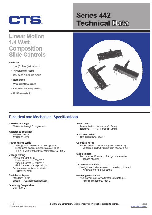
®Linear Motion 1/4 Watt Composition Slide Controls•11/4" (31.7mm) slider travel•1/4watt power rating •Choice of resistance tapers •Economical•Wide resistance range•Choice of mounting stylesElectrical and Mechanical SpecificationsResistance Range200 ohms through 5 megaohmsResistance ToleranceStandard:±20%Available:±10%Power Rating, Watts1/4watt @ 55°C derated to no load @ 85°C,linear taper, control mounted on steel panel4" x 4" x .050" (101.6mm x 101.6mm x 1.27mm). Voltage RatingAcross end terminals:Linear curves — 500 VDCTapered curves — 350 VDC(Not to exceed wattage ratings)Between case and end terminals:1080 VAC RMSResistance TapersStandard:LinearSpecial:Available upon request Slide TravelMechanical — 11/4inches (31.7mm)Effective — 11/4inches (31.7mm)Shaft InformationSee illustrations, page 2.Operating ForceEither direction 1 to 9 in-oz. (28 to 256 gf-cm)Measured .250" (6.35mm) from base of slider.Stop StrengthMaximum — 35 in-lbs. (15.9 kg-cm) measuredat base of slider.Terminal InformationStraight, vertical or snap-in to printed circuit board,wirewrap or solder lug styles.Mounting InformationTop, bottom, side or no twist tab mounting —refer to illustrations, page 2.FeaturesOperating Temperature0°C - +70°C•RoHS compliant1-2©2006CTS C orporati o n. A ll r i g hts r eserved. I nformati o n s ubject t o c hange.9/21/06 CTS Electronic Components Ordering Information CTS Series 442DIMENSION:mmINCHSUGGESTED PANEL PIERCING VIEWED FROM TOP SIDE FOR TWIST TABS AND ACTUATOR FROM TOP SIDE FOR TWIST TABS SUGGESTED PANEL PIERCING VIEWED2.03851.77SUGGESTED PANEL PIERCING VIEWED FROMCENTERLINE OF CONTROL FOR VERTICAL P.C. TERMINALS CONTROL SIDE FOR STRAIGHT P.C. & WIREWRAP TERMINALSSUGGESTED PANEL PIERCING VIEWED FROMALTERNATE TERMINAL STYLESNO MOUNT2-2©2006CTS C orporati o n. A ll r i g hts r eserved. I nformati o n s ubject t o c hange.9/21/06 CTS Electronic Components CONTROL SIDE FOR SNAP-IN P.C. TERMINALSSUGGESTED PANEL PIERCING VIEWED FROM。
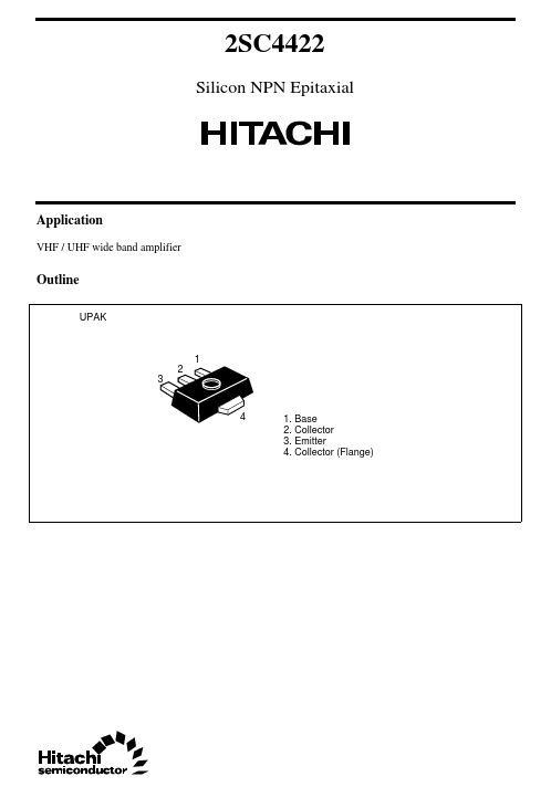
2SC4422中文资料
IMAG. –268.988 –221.759 –167.756 –133.425 –110.501 –94.442 –82.874 –73.836 –67.183 –61.241
Yre (mS) REAL 0.000 0.005 0.006 0.024 0.025 0.056 0.079 0.124 0.180 0.246
2.0 IE = 0 f = 1 MHz
1.6
1.2
0.8
0.4
0
1
2
5 10 20
50
Collector to Base Voltage VCB (V)
Power Gain PG (dB)
Power Gain vs. Collector Current
20 VCE = 0 f = 900 MHz
16
–0.2
–0.4 –0.6 –0.8 –1
–10
–5 –4 –3
–2 –1.5
6
Hale Waihona Puke S Parameters (Emitter Common)
Test Condition VCE = 5 V, IC = 5 mA, ZO = 50 Ω
Freq. (MHz) 100 200 300 400 500 600 700 800 900 1000
REAL
IMAG.
0.175
0.922
0.218
1.731
0.206
2.618
0.250
3.531
0.295
4.395
0.421
5.324
0.387
6.235
0.413
7.209
0.338
8.218
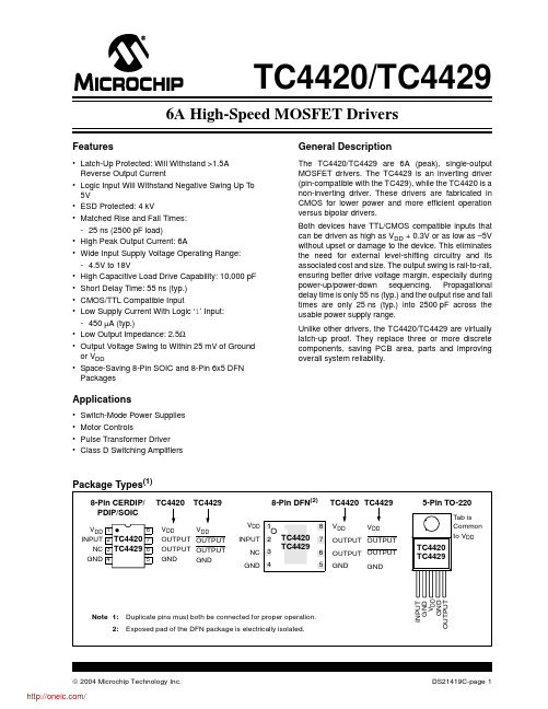
TC4429COA;TC4420COA;TC4429CPA;TC4420CPA;TC4420EPA;中文规格书,Datasheet资料
VDD Output
DS21419C-page 2
/
2004 Microchip Technology Inc.
1.0 ELECTRICAL CHARACTERISTICS
Absolute Maximum Ratings†
Supply Voltage ..................................................... +20V Input Voltage .................................. – 5V to VDD + 0.3V Input Current (VIN > VDD)................................... 50 mA Power Dissipation (TA ≤ 70°C)
- 4.5V to 18V • High Capacitive Load Drive Capability: 10,000 pF • Short Delay Time: 55 ns (typ.) • CMOS/TTL Compatible Input • Low Supply Current With Logic ‘1’ Input:
TC4420/TC4429
† Stresses above those listed under “Absolute Maximum Ratings” may cause permanent damage to the device. These are stress ratings only and functional operation of the device at these or any other conditions above those indicated in the operation sections of the specifications is not implied. Exposure to Absolute Maximum Rating conditions for extended periods may affect device reliability.
CLM4420资料
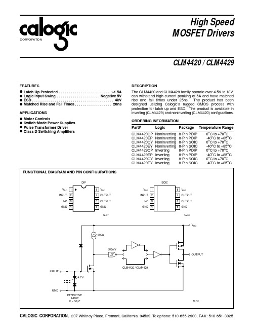
High Speed MOSFET Drivers CLM4420 / CLM4429FEATURES•Latch Up Protected. . . . . . . . . . . . . . . . . . . . . . . . . >1.5A •Logic Input Swing. . . . . . . . . . . . . . . . . . . . . Negative 5V •ESD. . . . . . . . . . . . . . . . . . . . . . . . . . . . . . . . . . . . . . . . 4kV •Matched Rise and Fall Times. . . . . . . . . . . . . . . . . . 20nsAPPLICATIONS•Motor Controls•Switch-Mode Power Supplies•Pulse Transformer Driver•Class D Switching Amplifiers DESCRIPTIONThe CLM4420 and CLM4429 family operate over 4.5V to 18V, can withstand high current peaking of 6A and have matched rise and fall times under 25ns. The product has been designed utilizing Calogic’s rugged CMOS process with protection for latch up and ESD. The product is available in inverting (CLM4429) and noninverting (CLM4420) configurations. ORDERING INFORMATIONPart#Logic Package Temperature Range CLM4420CP Noninverting8-Pin PDIP0C to +70C CLM4420EP Noninverting8-Pin PDIP-40o C to +85o C CLM4420CY Noninverting8-Pin SOIC0o C to +70o C CLM4420EY Noninverting8-Pin SOIC-40o C to +85o C CLM4429CP Inverting8-Pin PDIP0o C to +70o C CLM4429EP Inverting8-Pin PDIP-40o C to +85o C CLM4429CY Inverting8-Pin SOIC0o C to +70o C CLM4429EY Inverting8-Pin SOIC-40o C to +85oCABSOLUTE MAXIMUM RATINGSSupply Voltage. . . . . . . . . . . . . . . . . . . . . . . . . . . . . . . . +20V Input Voltage. . . . . . . . . . . . . . . . . . . . . . . . . . . . -5V to >V DD Input Current (V IN > V DD). . . . . . . . . . . . . . . . . . . . . . . . 50mA Power Dissipation, T A≤ 25o CPDIP. . . . . . . . . . . . . . . . . . . . . . . . . . . . . . . . . . . . . . . . 1W SOIC. . . . . . . . . . . . . . . . . . . . . . . . . . . . . . . . . . . 500mW Derating Factors (T o Ambient)PDIP . . . . . . . . . . . . . . . . . . . . . . . . . . . . . . . . . . . 8mW/o C SOIC. . . . . . . . . . . . . . . . . . . . . . . . . . . . . . . . . . . 4mW/o C Storage T emperature Range. . . . . . . . . . . . -55o C to +150o C Operating T emperature (Chip). . . . . . . . . . . . . . . . . . . +150o C Operating Temperature Range (Ambient)C Version. . . . . . . . . . . . . . . . . . . . . . . . . . . . 0o C to +70o C E Version. . . . . . . . . . . . . . . . . . . . . . . . . . -40o C to +85o C Lead Temperature (Soldering, 10 sec). . . . . . . . . . . . +300o C Static-sensitive device. Unused devices must be stored in conductive material. Protect devices from static discharge and static fields. Stresses above those listed under "Absolute Maximum Ratings" may cause permanent damage to the device. These are stress ratings only and functional operation of the device at these or any other conditions above those indicated in the operation sections of the specifications is not implied. Exposure to absolute maximum rating conditions for extended-periods may affect device reliability.ELECTRICAL CHARACTERISTICS: T A = +25o C with 4.5V ≤ V DD≤18V, unless otherwise specified.ELECTRICAL CHARACTERISTICS:Measured over operating temperature range with 4.5V ≤ V DD≤ 18V, unless otherwise specified.Note: 1. Switching times guaranteed by design.DIE SIZE 76 X 77 (INCHES)DD INV OUT GNDOUTGND GNDDDV DIE SIZE 76 X 77 (mm)。
- 1、下载文档前请自行甄别文档内容的完整性,平台不提供额外的编辑、内容补充、找答案等附加服务。
- 2、"仅部分预览"的文档,不可在线预览部分如存在完整性等问题,可反馈申请退款(可完整预览的文档不适用该条件!)。
- 3、如文档侵犯您的权益,请联系客服反馈,我们会尽快为您处理(人工客服工作时间:9:00-18:30)。
Power Transistors
2SC4420
Silicon NPN triple diffusion planar type
For high breakdown voltage high-speed switching
Unit: mm
q q q q q
16.2±0.5 12.5 3.5 Solder Dip
Thermal resistance Rth(t) (˚C/W)
1000
100 (1) 10 (2)
1
0.1 10–4
10–3
10–2
10–1
1
10
102
103
104
Time t (s)
3
VCE=5V f=1MHz TC=25˚C
Base to emitter saturation voltage VBE(sat) (V)
Forward current transfer ratio hFE
30
300
Transition frequency fT (MHz)
1 3 10
30
10
100 TC=100˚C 25˚C 10 –25˚C
0.1
0.3
1
3
10
Ambient temperature Ta (˚C)
Collector to emitter voltage VCE (V)
Collector current IC (A)
VBE(sat) — IC
100 1000 IC/IB=5
hFE — IC
VCE=5V 100
fT — IC
100 30 Non repetitive pulse TC=25˚C
Collector output capacitance Cob (pF)
Switching time ton,tstg,tf (µs)
300
Collector current IC (A)
10 3
10 3 1
ICM IC
100
t=0.1ms
1:Base 2:Collector 3:Emitter TOP–3 Full Pack Package(a)
s Electrical Characteristics
Parameter Collector cutoff current Emitter cutoff current Collector to emitter voltage Forward current transfer ratio Collector to emitter saturation voltage Base to emitter saturation voltage Transition frequency Turn-on time Storage time Fall time
IC — VCE
Collector to emitter saturation voltage VCE(sat) (V)
100 IC/IB=5 30 10 25˚C 3 1 0.3 0.1 0.03 0.01 0.01 0.03 –25˚C TC=100˚C
VCE(sat) — IC
Collector power dissipation PC (W)
High-speed switching High collector to base voltage VCBO Wide area of safe operation (ASO) Satisfactory linearity of foward current transfer ratio hFE Full-pack package which can be installed to the heat sink with one screw (TC=25˚C)
(TC=25˚C)
Symbol ICBO IEBO VCEO hFE1 hFE2 VCE(sat) VBE(sat) fT ton tstg tf Conditions VCB = 900V, IE = 0 VEB = 7V, IC = 0 IC = 10mA, IB = 0 VCE = 5V, IC = 0.1A VCE = 5V, IC = 0.8A IC = 0.8A, IB = 0.16A IC = 0.8A, IB = 0.16A VCE = 5V, IC = 0.15A, f = 1MHz IC = 0.8A, IB1 = 0.16A, IB2 = – 0.32A, VCC = 250V 10 0.7 2.5 0.3 800 8 6 1.5 1.5 V V MHz µs µs µs min typ max 50 50 Unit µA µA V
10
3
30
3
1 T =–25˚C C 100˚C 0.3 25˚C
1
3
0.3
0.1 0.01 0.03
0.1
0.3
1
3
10
1 0.01 0.03
0.1
0.3
0.1 0.01 0.03
0.1
0.3
1
3
10
Collector current IC (A)
Collector current IC (A)
Collector current IC (A)
Vclamp
Collector to emitter voltage VCE (Vmeasured at Ta=25˚C and under natural convection. (1) PT=10V × 0.2A (2W) and without heat sink (2) PT=10V × 1.0A (10W) and with a 100 × 100 × 2mm Al heat sink
tstg 1 0.3 tf 0.1 0.03 ton
30
1ms 0.3 0.1 0.03 0.01 10ms DC
10
3
1 1 3 10 30 100
0.01 0 0.4 0.8 1.2 1.6
1
3
10
30
100
300
1000
Collector to base voltage VCB (V)
Collector current IC (A)
2SC4420
Reverse bias ASO measuring circuit
L coil IB1 Vin T.U.T IC
Collector current IC (A)
12 10 8 6 4 2 0 0 200 400 600 800 1000 1200 1400 1600
–IB2
VCC
tW
70 60 50 40 30 20 10
2.5
IB=500mA 400mA
Collector current IC (A)
2.0
300mA 200mA
1.5
1.0
100mA 50mA
(2)
0.5 (3) 0 0 20 40 60 80 100 120 140 160 0 0 2 4 6 8 10 12
Cob — VCB
1000 100 IE=0 f=1MHz TC=25˚C 30
ton, tstg, tf — IC
Pulsed tw=1ms Duty cycle=1% IC/IB=5 (2IB1=–IB2) VCC=250V TC=25˚C
Area of safe operation (ASO)
Ratings 900 900 800 7 5 3 1 70 3 150 –55 to +150 Unit V V V V A A A W ˚C ˚C
0.7
s Features
15.0±0.3 11.0±0.2
5.0±0.2 3.2
21.0±0.5 15.0±0.2
φ3.2±0.1
2.0±0.2 2.0±0.1 1.1±0.1 5.45±0.3 10.9±0.5 1 2 3 0.6±0.2
s Absolute Maximum Ratings
Parameter Collector to base voltage Collector to emitter voltage Emitter to base voltage Peak collector current Collector current Base current Collector power TC=25°C dissipation Ta=25°C Junction temperature Storage temperature Symbol VCBO VCES VCEO VEBO ICP IC IB PC Tj Tstg
Collector to emitter voltage VCE (V)
2
元器件交易网
Power Transistors
Area of safe operation, reverse bias ASO
16 14 Lcoil=200µH IC/IB=5 (IB1=–IB2) TC=25˚C
1
元器件交易网
Power Transistors
PC — Ta
80 3.0 TC=25˚C (1) (1) TC=Ta (2) With a 100 × 100 × 2mm Al heat sink (3) Without heat sink (PC=3W)
2SC4420