BL-PDO-CRS-C10中文资料
BL-PWT-SJS-C10中文资料
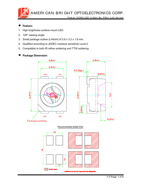
• Feature:1. High brightness surface mount LED.2. 120° viewing angle.3. Small package outline (LxWxH) of 2.8 x 3.2 x 1.8 mm.4. Qualified according to JEDEC moisture sensitivity Level 2.5. Compatible to both IR reflow soldering and TTW soldering. • Package Dimension:Recommended Solder Pad• Optical Characteristics:Part Number Chip TechnologyColor ViewingAngleLuminous Intensity @ If @ 30mAIv ( mcd )BL-PWB-SJS-C20 • BIN Q2• BIN R1• BIN R2BL-PWB-SJS-C10 • BIN R1• BIN R2• BIN S1BL-PWB-UJS-C10 • BIN R2• BIN S1• BIN S2InGaN /Blue, 470 nm12090.0 … 180.090.0 … 112.5112.5 … 140.0140.0 … 180.0112.5 … 224.0112.5 … 140.0140.0 … 180.0180.0 … 224.0140.0 … 285.0140.0 … 180.0180.0 … 224.0224.0 … 285.0BL-PWC-CJS-C10 • BIN S1• BIN S2• BIN T1• BIN T2BL-PWC-SJS-C10 • BIN T1• BIN T2• BIN U1• BIN U2BL-PWC-SJS-C20 • BIN U1• BIN U2• BIN V1• BIN V2BL-PWC-UJS-C10 • BIN U1• BIN U2• BIN V1• BIN V2 InGaN /Cyan, 505nm120180.0 … 450.0180.0 … 224.0224.0 … 285.0285.0 … 355.0355.0 … 450.0285.0 … 715.0285.0 … 355.0355.0 … 450.0450.0 … 560.0560.0 … 715.0450.0 … 1125.0450.0 … 560.0560.0 … 715.0715.0 … 900.0900.0 … 1125.0450.0 … 1125.0450.0 … 560.0560.0 … 715.0715.0 … 900.0900.0 … 1125.0• Optical Characteristics:Part Number Chip TechnologyColor ViewingAngleLuminous Intensity @ If @ 30mAIv ( mcd )BL-PWT-CJS-C10 • BIN S1• BIN S2• BIN T1• BIN T2BL-PWT-SJS-C10 • BIN T1• BIN T2• BIN U1• BIN U2 BL-PWT-SJS-C20 • BIN U1• BIN U2• BIN V1• BIN V2 BL-PWT-UJS-C10 • BIN U1• BIN U2• BIN V1• BIN V2 InGaN /True Green, 525nm120 180.0 … 450.0180.0 … 224.0224.0 … 285.0285.0 … 355.0355.0 … 450.0285.0 … 715.0285.0 … 355.0355.0 … 450.0450.0 … 560.0560.0 … 715.0450.0 … 1125.0450.0 … 560.0560.0 … 715.0715.0 … 900.0900.0 … 1125.0450.0 … 1125.0450.0 … 560.0560.0 … 715.0715.0 … 900.0900.0 … 1125.0BL-PWW-SJD-C10 • BIN T1• BIN T2• BIN U1• BIN U2BL-PWW-UJD-C10 • BIN U1• BIN U2• BIN V1• BIN V2 InGaN /White (0.31, 0.31)120 285.0 … 715.0285.0 … 355.0355.0 … 450.0450.0 … 560.0560.0 … 715.0450.0 … 1125.0450.0 … 560.0560.0 … 715.0715.0 … 900.0900.0 … 1125.0Note:1. Other luminous intensity groups are also available upon request.2. Luminous intensity is measured with an accuracy of ±11%.3. Wavelength binning is carried for all units as per the wavelength-binning table. Only one wavelengthgroup is allowed for each reel.4. InGaN wavelength is very sensitive to drive current. Operating at lower current is not recommendedand may yield unpredictable performance Current pulsing should be used for dimming purposes.5. An optional Vf binning is also available upon request. Binning scheme is as per following table.• Absolute Maximum Ratings:Parameter Maximum Value Unit DC forward current. 30 mA Peak pulse current; (tp ≤ 10 µs, Duty cycle = 0.005) 200 mA Reverse voltage; Ir (max) = 10µA. 5 V LED junction temperature. 125 °C Operating temperature. -40 … +100 °C Storage temperature. -40 … +100 °C Power dissipation ( at room temperature ) 135 mW • Vf Binning:Vf Bin @ 30mA Forward voltage (V)Standard 3.9 (typical), 4.55 (max)30 3.35 … 3.6531 3.65 … 3.9532 3.95 … 4.2533 4.25 … 4.55Forward voltage, Vf is measured with an accuracy of ±01 V.• Wavelength Grouping:Color Group Wavelength (nm) @ 30mABL-PWB; Blue FullWXYZ 464 - 476 464 - 468 468 - 472 472 – 476 476 - 480BL-PWC; Cyan FullWXY 499 - 511 499 - 503 503 - 507 507 - 511BL-PWT; True Green FullWXYZ 520- 536 520 - 524 524 - 528 528 – 532 532 – 536Wavelength is measured with an accuracy of ±1 nm.•Bin X Bin WA1 Cx 0.2775 0.2900 0.29000.2775E1 Cx 0.32750.3400 0.3400 0.3275Cy 0.2732 0.2939 0.31140.2907 Cy 0.35610.3768 0.3943 0.3736 A2 Cx 0.2775 0.2900 0.29000.2775E2 Cx 0.32750.3400 0.3400 0.3275Cy 0.2557 0.2764 0.29390.2732 Cy 0.33860.3593 0.3768 0.3561 A3 Cx 0.2900 0.3025 0.30250.2900E3 Cx 0.34000.3525 0.3525 0.3400Cy 0.2939 0.3146 0.33210.3114 Cy 0.37680.3975 0.4150 0.3943 A4 Cx 0.2900 0.3025 0.30250.2900E4 Cx 0.34000.3525 0.3525 0.3400Cy 0.2764 0.2971 0.31460.2939 Cy 0.35930.3800 0.3975 0.3768 C1 Cx 0.3025 0.3150 0.31500.3025Cy 0.3146 0.3354 0.35290.3321C2 Cx 0.3025 0.3150 0.31500.3025Cy 0.2971 0.3179 0.33540.3146C3 Cx 0.3150 0.3275 0.32750.3150Cy 0.3354 0.3561 0.37360.3529C4 Cx 0.3150 0.3275 0.32750.3150Cy 0.3179 0.3386 0.35610.3354• Typical electro-optical characteristics curves:Fig.1 Relative luminous intensity vs. forward current. Fig.2 Forward current vs. forward voltage.Fig.3 Radiation pattern.Fig.4 Maximum forward current vs. temperature.Fig.5 Relative Intensity vs Wavelength Fig.6 Dominant Wavelength vs Forward CurrentFig. 7 Recommended IR-reflow Soldering Profile.Fig. 8 Recommended TTW Soldering Profile.• Taping And Orientation:Reels come in quantity of 2000 units.Reel diameter is 180 mm.。
MAX-M10S u-blox M10高精度GNSS模块数据手册说明书

MAX-M10Su-blox M10 standard precision GNSS moduleData sheetAbstractThis document describes the features and application of the MAX-M10S,an ultra-low-power GNSS receiver for high-performance asset-trackingdevices.UBX-20035208 - R01C1-PublicDocument informationTitle MAX-M10SSubtitle u-blox M10 standard precision GNSS moduleDocument type Data sheetDocument number UBX-20035208Revision and date R0121-Dec-2020 Document status Objective specificationDisclosure restriction C1-PublicProduct status Corresponding content statusIn development /Objective specification Target values. Revised and supplementary data will be published later. prototypeEngineering sample Advance information Data based on early testing. Revised and supplementary data will bepublished later.Initial production Early production information Data from product verification. Revised and supplementary data may bepublished later.Mass production /Production information Document contains the final product specification.End of lifeThis document applies to the following products:Product name Type number Firmware version PCN referenceMAX-M10S MAX-M10S-00B-00SPG 5.00N/Au-blox reserves all rights to this document and the information contained herein. Products, names, logos and designs described herein may in whole or in part be subject to intellectual property rights. Reproduction, use, modification or disclosure to third parties of this document or any part thereof without the express permission of u-blox is strictly prohibited. The information contained herein is provided "as is" and u-blox assumes no liability for the use of the information. No warranty, either express or implied, is given with respect to, including but not limited to, the accuracy, correctness, reliability and fitness for a particular purpose of the information. This document may be revised by u-blox at any time. For most recent documents, please visit www.u .Copyright © 2020, u-blox AG.u-blox is a registered trademark of u-blox Holding AG in the EU and other countries.Contents1 Functional description (4)1.1 Overview (4)1.2 Performance (4)1.3 Supported GNSS constellations (5)1.4 Supported protocols (6)1.5 Firmware features (6)2 System description (7)2.1 Block diagram (7)3 Pin definition (8)3.1 Pin assignment (8)4 Electrical specification (10)4.1 Absolute maximum ratings (10)4.2 Operating conditions (10)4.3 Indicative power requirements (11)5 Communication interfaces (13)5.1 UART (13)5.2 I2C (13)5.3 Default interface settings (13)6 Mechanical specification (14)7 Labeling and ordering information (15)7.1 Product labeling (15)7.2 Explanation of product codes (15)7.3 Ordering codes (15)Related documents (17)Revision history (18)1 Functional description1.1 OverviewThe MAX-M10S module features the u-blox M10 standard precision GNSS platform and provides exceptional sensitivity and acquisition times for all L1 GNSS signals.The extremely low power consumption in continuous tracking mode allows great power autonomy for all battery-operated devices, such as asset trackers, without compromising on GNSS performance.The MAX-M10S supports concurrent reception of up to four GNSS (GPS, GLONASS, Galileo, and BeiDou). The high number of visible satellites enables the receiver to select the best signals. This maximizes the position accuracy, in particular under challenging conditions such as in deep urban canyons. In the firmware described here, however, the number of concurrently received GNSS is limited to three. u-blox Super-S (Super-Signal) technology offers great RF sensitivity.The MAX-M10S integrates an LNA followed by a SAW filter in the RF path for maximum sensitivity in passive antenna designs.The MAX-M10S offers backwards pin-to-pin compatibility with products from the previous u-blox generations, which saves the designer's effort and reduces costs when upgrading designs.The MAX-M10S is based on the u-blox M10 GNSS chip, which is qualified according to AEC-Q100, manufactured in IATF 16949 certified sites, and fully tested on a system level.1.2 PerformanceParameter SpecificationReceiver type u-blox M10 receiverAccuracy of time pulse signal RMS99%30 ns60 nsFrequency of time pulse signal 0.25 Hz to 10 MHz (configurable)Operational limits1Dynamics≤ 4 gAltitude80,000 mVelocity500 m/sVelocity accuracy20.05 m/sDynamic heading accuracy20.3 degGNSS GPS+GAL GPS+GLO GPS+BDS GPS+GLO+GAL GPS+GAL+BDSAcquisition3Cold startHot startAided start429 s1 s1 s26 s1 s1 s27 s1 s1 s24 s1 s1 s27 s1 s1 sNav. update rate PVT10 Hz10 Hz10 Hz10 Hz10 Hz1Assuming Airborne 4 g platform250% at 30 m/s for dynamic operation3Commanded starts. All satellites at -130 dBm. GPS always in combination with QZSS and SBAS. Measured at room temperature.4Dependent on the speed and latency of the aiding data connection, commanded starts.GNSS GPS+GAL GPS+GLO GPS+BDS GPS+GLO+GAL GPS+GAL+BDSSensitivity5Tracking and nav.ReacquisitionCold startHot start -166 dBm-160 dBm-148 dBm-160 dBm-167 dBm-160 dBm-148 dBm-160 dBm-167 dBm-160 dBm-148 dBm-160 dBm-167 dBm-160 dBm-148 dBm-160 dBm-166 dBm-160 dBm-148 dBm-160 dBmPosition accuracy PVT 2 m CEP 2 m CEP 2 m CEP 2 m CEP 2 m CEP Table 1: MAX-M10S typical performance in multi-constellation GNSS modesGNSS GPS GLONASS BEIDOU GALILEOAcquisition3Cold startHot startAided start429 s1 s1 s27 s1 s1 s30 s1 s1 s38 s1 s5 sNav. update rate PVT18 Hz18 Hz18 Hz18 HzSensitivity5Tracking and nav.ReacquisitionCold startHot start -166 dBm-160 dBm-148 dBm-160 dBm-166 dBm-154 dBm-147 dBm-156 dBm-160 dBm-158 dBm-146 dBm-159 dBm-159 dBm-154 dBm-141 dBm-154 dBmPosition accuracy PVT 2 m CEP 4 m CEP 3 m CEP 3 m CEPTable 2: MAX-M10S typical performance in single-GNSS modes1.3 Supported GNSS constellationsThe MAX-M10S is a concurrent GNSS receiver which can receive and track multiple GNSS systems. The single RF front-end architecture enables all major GNSS constellations to be received concurrently. The receiver can be configured for a sub-set of GNSS constellations to achieve lower power consumption.The following GNSS and their signals are supported:System SignalsGPS L1C/A (1575.42 MHz)Galileo E1-B/C (1575.42 MHz)GLONASS L1OF (1602 MHz + k*562.5 kHz, k = –7,..., 5, 6)BeiDou B1I (1561.098 MHz)Table 3: Supported GNSS and signals on MAX-M10SThe following GNSS assistance services are supported:Service SupportAssistNow™ Online SupportedAssistNow™ Offline SupportedAssistNow™ Autonomous SupportedTable 4: Supported Assisted GNSS (A-GNSS) servicesThe following augmentation systems are supported:5Demonstrated with a good external LNA. Measured at room temperature.System SupportSBAS EGNOS, GAGAN, MSAS and WAASQZSS L1S (SLAS)Table 5: Supported augmentation systemsThe augmentation systems SBAS and QZSS can be enabled only if GPS operation is also enabled.1.4 Supported protocolsThe MAX-M10S supports the following protocols:Protocol TypeUBX Input/output, binary, u-blox proprietaryNMEA versions 2.1, 2.3, 4.0, and 4.10. (default 4.10)Input/output, ASCIITable 6: Supported protocols1.5 Firmware featuresFeature DescriptionAntenna supervisor6Active antenna supervisor to detect short and open statusAssisted GNSS AssistNow Online, AssistNow Offline and AssistNow Autonomous supported Backup modes Hardware backup mode, hardware standby mode, software standby mode (similar toolder software backup mode), all with optional RTCData batching Autonomous tracking up to 5 minutes at 1 HzOdometer Measure traveled distance with support for different user profilesTable 7: Firmware featuresFeature DescriptionAnti-jamming RF interference and jamming detection and reporting; Active GNSS in-band filtering Anti-spoofing Spoofing detection and reportingMessage integrity All messages are cryptographically signed, JTAG debug interface disabled by default Table 8: Security features6External components required, some pins need to be reprogrammed as needed.2 System description2.1 Block diagramFigure 1: MAX-M10S block diagramThe GPIOs can be programmed for different uses like external interrupt, enable LNA, TX ready, data batching indicator, and antenna supervisor.3 Pin definition3.1 Pin assignmentThe pin assignment of the MAX-M10S module is shown below:Figure 2: MAX-M10S pin assignmentPin PIO no.I/O Description1GND--Connect to GND2TXD1O UART TX3RXD0I UART RX4TIMEPULSE4O Time pulse signal5EXTINT5I External interrupt6V_BCKP-I Backup voltage supply7V_IO-I IO voltage supply8VCC-I Main voltage supply9RESET_N-I System reset (active low)10GND--Connect to GND11RF_IN-I GNSS signal input12GND--Connect to GND13LNA_EN-O On/Off external LNA or active antenna 14VCC_RF-O Output voltage RF section15Reserved--Reserved16SDA2I/O I2C data17SCL3I I2C clockPin PIO no.I/O Description18SAFEBOOT_N-I Safeboot mode (leave OPEN) Table 9: MAX-M10S pin assignment4 Electrical specificationThe limiting values given are in accordance with the Absolute Maximum Rating System(IEC 134). Stress above one or more of the limiting values may cause permanent damageto the device. These are stress ratings only. Operation of the device at these or at any other conditions above those given below is not implied. Exposure to limiting values for extended periods may affect device reliability.Where application information is given, it is advisory only and does not form part of thespecification.4.1 Absolute maximum ratingsSymbol Parameter Min Max UnitVCC Supply voltage–0.3 3.6VVoltage ramp on VCC72535000µs/VV_IO Supply voltage, I/O–0.3 3.6VVoltage ramp on V_IO72535000µs/VV_BCKP Supply voltage, backup domain–0.3 3.6VVoltage ramp on V_BCKP725µs/VVin Input voltage, digital pins–0.3V_IO + 0.3V(max 3.6)Ipin Max source / sink current, digital pins8-1010mAICC_RF Max source current, VCC_RF100mAP rfin RF input power on RF_IN9+15dBmT amb Ambient temperature–40+85°CT s Storage temperature–40+85°CTable 10: Absolute maximum ratingsThe product is not protected against overvoltage or reversed voltages. Voltage spikesexceeding the power supply voltage specification, given in the table above, must be limited to values within the specified boundaries by using appropriate protection diodes.4.2 Operating conditionsTable 11shows the general operating conditions. Table 12shows the electrical parameters for digital I/O.Symbol Parameter Min Typical Max UnitsVCC Supply voltage 2.7 3.0 3.6VV_IO Supply voltage, I/O 2.7 3.0 3.6VV_BCKP Supply voltage, backup domain 1.65 3.6VVCC_RF VCC_RF output voltage VCC-0.1VICC_RF VCC_RF output current50mANF tot Receiver chain noise figure2dB7Exceeding the voltage ramp speed may permanently damage the device.8SAFEBOOT_N pin has an internal 1 kΩ series resistor. With a 3.3 V supply, the current is limited to 3.3 mA.9Test conditions TBCSymbol Parameter Min Typical Max UnitsExt_gain10External gain at RF_IN, low gain mode (default)TBD dBExternal gain at RF_IN, bypass mode TBD dBT opr Operating temperature-40+85°CTable 11: General operating conditionsSymbol Parameter Min Typical Max UnitsV in Input pin voltage range0V_IO VV il Low-level input voltage0.63VV ih High-level input voltage0.68 x V_IO VV ol Low-level output voltage, Iout = -2 mA0.4VV oh High-level output voltage, Iout = 2 mA V_IO - 0.4VR pu, IO Pull-up resistance, Digital IO1151772kΩR pu, SAFEBOOT_N Pull-up resistance, SAFEBOOT_N1251772kΩR pu, RESET_N Pull-up resistance, RESET_N71013kΩTable 12: Digital IOOperation beyond the specified operating conditions can affect device reliability.To trigger a reset, the minimum low period for RESET_N is 1 ms.4.3 Indicative power requirementsTable 13 lists examples of the total system supply current for VCC and V_IO. Table 14 shows current consumptions for the backup modes.These values are provided for customer information only, as an example of typical current requirements. They are characterized on samples using a cold start command. Actualpower requirements can vary depending on FW version used, external circuitry, number of satellites tracked, signal strength, type and time of start, duration, internal LNA gain mode, and test conditions.Symbol Parameter Conditions GPS GPS+GAL GPS+GAL+GLO GPS+GAL+BEIUnitI PEAK Peak current Acquisition25252525mAAcquisition 6.57.09.010.5mA I VCC13Current at VCCTracking(Continuous mode)6.0 6.07.08.0mAAcquisition 2.2 2.2 2.3 2.3mA I V_IO14Current at V_IOTracking(Continuous mode)2.2 2.2 2.3 2.3mA Table 13: Typical currents to calculate the indicative power requirementsSymbol Parameter Conditions Typ.Unit I V_BCKP Total current in hardware backup mode V_BCKP = 3.3 V / V_IO = VCC = 0 V32µA 10The internal LNA gain is configurable.11TXD, RXD, TIMEPULSE, EXTINT, SCL, SDA, and LNA_EN.12The SAFEBOOT_N pin has an additional 1 kΩ series resistor.13Voltage at VCC = 3.0 V. Internal LNA set to low gain. Simulated signal using power levels of -130 dBm.14Voltage at V_IO = 3.0 V.Symbol Parameter Conditions Typ.Unit Total current in hardware standby mode V_IO = 3.3 V / VCC = 0 V46µAI VCC, V_IO15Total current in software standby mode V_IO = 3.3 V / VCC = 3.3 V TBDµA Table 14: Backup currents to calculate the indicative power requirementsAll values in Table 13 and Table 14 are measured at 25 °C ambient temperature and with the internal LNA set to low gain.SBAS and QZSS are activated in all measurements.15I VCC, V_IO includes currents flowing into VCC and V_IO.5 Communication interfacesThe receiver allows communication over UART and I2C16 interface.All the inputs have internal pull-up resistors in normal operation and can be left open if not used. All the PIOs are supplied by V_IO, therefore all the voltage levels of the PIO pins are related to V_IO supply voltage.5.1 UARTThe UART interface supports configurable baud rates. Hardware flow control is not supported.Symbol Parameter Min Max UnitR u Baud rate4800921600bit/sΔTx Tx baud rate accuracy-1%+1%-ΔRx Rx baud rate tolerance-2.5%+2.5%-Table 15: UART specifications5.2 I2CAn I2C-compliant interface is available for communication with an external host CPU. The interface is compatible with the Fast-mode of the I2C industry standard, allowing a maximum bit rate of 400 kbit/s17.5.3 Default interface settingsInterface SettingsUART•9600 baud, 8 bits, no parity bit, 1 stop bit.•Input messages: NMEA and UBX.•Output messages: NMEA GGA, GLL, GSA, GSV, RMC, VTG and TXT.I2C•7-bit I2C address (0x42).•Input messages: NMEA and UBX.•Output messages: NMEA GGA, GLL, GSA, GSV, RMC, VTG and TXT.Table 16: Default interface settings16I2C is a registered trademark of Philips/NXP.17External pull-up resistors are needed to achieve 400 kbit/s communication speed as the internal pull-up resistance can be very large.6 Mechanical specificationFigure 3: MAX-M10S mechanical drawing7 Labeling and ordering informationThis section provides information about product labeling and ordering.7.1 Product labelingThe labeling of the MAX-M10S package provides product information and revision information. For more information contact u-blox sales.Figure 4: Location of product type number on MAX-M10S label7.2 Explanation of product codesThree product code formats are used. The Product name is used in documentation such as this data sheet and identifies all u-blox products, independent of packaging and quality grade. The Ordering code includes options and quality, while the Type number includes the hardware and firmware versions.Table 17 details these three different formats for the MAX-M10S.Format Structure Product codeProduct name PPP-TGGV MAX-M10SOrdering code PPP-TGGV-NNQ MAX-M10S-00BType number PPP-TGGV-NNQ-XX MAX-M10S-00B-00Table 17: Product code formatsThe parts of the product code are explained in Table 18 .Code Meaning ExamplePPP Product family MAXTGG Platform M10 = u-blox M10V Variant S = Standard precision, ROM, LNA, and SAW filterNNQ Option / Quality grade NN: Option [00...99]Q: Grade, A = Automotive, B = ProfessionalXX Product detail Describes hardware and firmware versionsTable 18: Part identification code7.3 Ordering codesOrdering code Product RemarkMAX-M10S-00B u-blox MAX-M10S module, professional gradeTable 19: Product ordering codesProduct changes affecting form, fit or function are documented by u-blox. For a list ofProduct Change Notifications (PCNs) see our website at: https:///en/product-resources.UBX-20035208 - R017 Labeling and ordering information Page 16 of 19Related documents[1]MAX-M10S Integration manual, UBX-20053088[2]u-blox M10 SPG 5.00 Interface description, UBX-20048810For regular updates to u-blox documentation and to receive product change notifications please register on our homepage https://.UBX-20035208 - R01Related documents Page 17 of 19Revision historyRevision Date Name Status / comments 0121-Dec-2020imar, jesk, msul, rmak Objective specificationContactFor complete contact information visit us at .u-blox OfficesNorth, Central and South America Headquarters Asia, Australia, PacificEurope, Middle East, Africau-blox America, Inc.u-blox AG u-blox Singapore Pte. Ltd.Phone:+1 703 483 3180Phone:+41 44 722 74 44Phone:+65 6734 3811E-mail:******************E-mail:***************E-mail:******************Support:******************Support:********************* Regional Office West Coast Regional Office AustraliaPhone:+1 408 573 3640 Phone:+61 3 9566 7255E-mail:****************** E-mail:*******************Support:********************* Technical Support Regional Office China (Beijing) Phone:+1 703 483 3185 Phone:+86 10 68 133 545E-mail:********************* E-mail:******************Support:********************* Regional Office China (Chongqing) Phone:+86 23 6815 1588E-mail:******************Support:********************* Regional Office China (Shanghai)Phone:+86 21 6090 4832E-mail:******************Support:********************* Regional Office China (Shenzhen) Phone:+86 755 8627 1083E-mail:******************Support:********************* Regional Office IndiaPhone:+91 80 4050 9200E-mail:******************Support:********************* Regional Office Japan (Osaka)Phone:+81 6 6941 3660E-mail:******************Support:********************* Regional Office Japan (Tokyo)Phone:+81 3 5775 3850E-mail:******************Support:********************* Regional Office KoreaPhone:+82 2 542 0861E-mail:******************Support:********************* Regional Office TaiwanPhone:+886 2 2657 1090E-mail:******************Support:*********************。
读码器教学

激光条码读取器BL-1300 系列附录1 BL-1300 系列技术规格.....................................................................................A-2 技术规格............................................................................................................................. A-2读取范围特性(典型)........................................................................................................ A-4角度特性(典型)............................................................................................................... A-82 N-R2/R4/UB/L1 技术规格.................................................................................A-93 NX-50 系列技术规格.......................................................................................A-104 尺寸图............................................................................................................. A-125 一般故障排除..................................................................................................A-17 无法读取条码....................................................................................................... A-17读取率测试模式不是100%。
FM8413-LC条码扫码引擎硬件使用手册说明书

FM8413-LC 条码扫码引擎硬件使用手册2019. 12本资料是为了让用户根据用途选择合适的上海复旦微电子集团股份有限公司(以下简称复旦微电子)的产品而提供的参考资料,不转让属于复旦微电子或者第三者所有的知识产权以及其他权利的许可。
在使用本资料所记载的信息最终做出有关信息和产品是否适用的判断前,请您务必将所有信息作为一个整体系统来进行评价。
采购方对于选择与使用本文描述的复旦微电子的产品和服务全权负责,复旦微电子不承担采购方选择与使用本文描述的产品和服务的责任。
除非以书面形式明确地认可,复旦微电子的产品不推荐、不授权、不担保用于包括军事、航空、航天、救生及生命维持系统在内的,由于失效或故障可能导致人身伤亡、严重的财产或环境损失的产品或系统中。
未经复旦微电子的许可,不得翻印或者复制全部或部分本资料的内容。
今后日常的产品更新会在适当的时候发布,恕不另行通知。
在购买本资料所记载的产品时,请预先向复旦微电子在当地的销售办事处确认最新信息,并请您通过各种方式关注复旦微电子公布的信息,包括复旦微电子的网站(/)。
如果您需要了解有关本资料所记载的信息或产品的详情,请与上海复旦微电子集团股份有限公司在当地的销售办事处联系。
商标上海复旦微电子集团股份有限公司的公司名称、徽标以及“复旦”徽标均为上海复旦微电子集团股份有限公司及其分公司在中国的商标或注册商标。
上海复旦微电子集团股份有限公司在中国发布,版权所有。
目录目录1产品综述 (4)1.1产品简介 (4)1.2产品特点 (4)1.3外观及结构 (4)1.4典型应用 (5)2使用注意事项 (6)2.1ESD防护 (6)2.2镜头防护 (6)2.3工作条件 (6)2.4散热 (6)3电气特性 (7)3.1工作电源要求 (7)3.2直流特性 (7)3.2语音特性 (7)4接口说明 (8)4.1FPC柔性软排线接口 (8)4.2线到板连接器 (9)4.3USB连接器 (9)4.4通讯接口 (10)4.4.1串口 (10)4.4.2 USB (10)4.5状态指示输出 (10)4.5.1蜂鸣器输出 (10)4.5.2指示灯输出 (10)4.6触发信号输入 (11)4.7语音输出接口 (11)版本信息 (12)上海复旦微电子集团股份有限公司销售及服务网点 (13)1产品综述1.1产品简介FM8413条码扫码引擎是复旦微提供的条码识读解决方案,用于识别常用的纸张以及手机屏幕显示的主流QR码,模组分为嵌入式模块和整机集成模块,嵌入式模块体积小巧,装配灵活,对外提供丰富的接口以满足用户的定制化需求,可满足大部分嵌入式设备的应用场景;集成模块结构更加完整,提供统一的接口,增强了设备的安全防护特性,用于对结构尺寸限制较少,快速应用的场景。
实创兴SEW270模块用户技术手册V2.0

2
SEW270 WCDMA 模块
前言
概述
本文档适用的产品是:实创兴 SEW270 模块。本文档通过对 SEW270 模块的介绍,用以指导用户 对该模块进行硬件设计并获取软件技术支持,并在该模块基础上更方便快捷的进行各种终端无线产品 的设计。
阅读对象
本文档主要适用于以下工程师: � � � � � 系统设计工程师 结构工程师 硬件工程师 软件工程师 测试工程师
内容简介
本文档包含 5 章,内容如下: 章节 1 概述 2 产品介绍 3 引脚描述 4 硬件接口描述 5 结构 内容 介绍 SEW270 模块的基本技术规格、参考涉及的相关文档和缩略语。 简要介绍 SEW270 模块的电路原理图和应用方框图。 介绍 SEW270 模块引脚名称和功能。 介绍 SEW270 模块各部分的硬件接口参考设计。 介绍 SEW270 模块的外观图、装配图、天线连接器规格和模块固定方式。
侵权必究。 实创兴电子保留修改本手册技术参数及规格的权力,对本手册中的印刷错误及与最新资料不符之处我 们 会及时改进。所有这些改动不再事先通知,但会编入新版手册中。 实创兴电子拥有本手册的最终解释权。
1
SEW270 WCDMA 模块
实创兴是国内领先的移动通讯企业,以数据卡、移动手持终端、无线通讯模块解决方案为主营业务, 可为 WCDMA/EDGE/cdma2000 等通讯模块用户提供技术支持。 实创兴电子为客户提供现场、电话、网站、即时通讯、E-MAIL 等多种支持方式。 实创兴电子网站 ,提供相关的行业信息和模块相关技术资料。 全国技术支持您想获得实创兴电子产品的技术支持信息,您可以进入在线帮助,通过网络的方式与技 术支持进行交流。如有疑问可发送邮件至 support_Module@ 来获得技术支持。 技术支持热(2012-07-28) 第一次正式发布。 V2.0(2012-9-8) 修改 UIM 卡接口电路,修改模块复位功能实现方式,更新规格参数表。
C1010中文资料
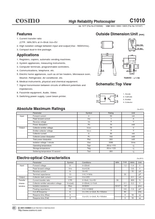
Schematic:Top View
Absolute Maximum Ratings
Parameter Input Forward current Peak forward current Reverse voltage Power dissipation Output Collector-emitter voltage Emitter-collector voltage Collector current Collector power dissipation Total power dissipation Isolation voltage 1 minute Operating temperature Storage temperature Soldering temperature 10 second Symbol IF IFM VR PD VCEO VECO IC PC Ptot Viso Topr Tstg Tsol Rating 50 1 6 70 70 6 50 150 200 5000 -30 to +115 -55 to +125 260 Unit mA A V mW V V mA mW mW Vrms °C °C °C
Collector Current Ic (mA)
Forward Current IF (mA)
Ambient Temperature Ta (°C)
Ambient Temperature Ta (°C)
c
2004
cosmo ELECTRONICS CORPORATION
Fig.7 Relative Current Transfer Ratio vs. Ambient Temperature
亿维自动化 X系列BD扩展板使用说明书
3.4. X-2AO-BD 产品说明书 ............................................................................................................ 19
3.4.1. 产品概述 ............................................................................................................................ 19
2.1.4. 模拟量 BD 扩展板地址对照表........................................................................................... 7
3. BD 扩展板详细参数..................................................................................................................................... 9
服务热线:4000 300 890
3.1.4. 安装及接线图 .................................................................................................................... 10
3.1.5. 应用说明 .............................................................................................................................11
万能红外遥控解码模块
/item.htm?id=7693624806该模块采用5V电源供电,可以完成目前应用最广泛的多种红外遥控编码的解码,包括飞利浦(RC5)编码(典型编码芯片如SAA3010及兼容芯片如PT2210 等)和NEC编码(典型编码芯片如uPD6121,uPD6122, TC9012 )以及众多的兼容芯片型号,(如PT2221, PT2222, SC6121, SC6122,SC9012 等等),采用该模块,可以缩短开发时间,节约CPU 资源,降低总体成本。
特点●使用简单、可靠● 支持多种编码● 兼容SPI 及UART(波特率9600)的串行输出● 采用数字滤波技术,高抗干扰,无误码● 接收有效指示输出● 工业级温度范围红外编码介绍目前应用于家电等领域的红外线遥控装置,并没有统一的国际标准,目前市场上所见的红外线遥控编码芯片,超过10 种之多,分别由飞利浦公司、NEC 公司、SONY 公司、东芝公司、三菱公司、JVC 公司等生产,使用的编码方式各不相同。
目前应用最广泛、兼容产品最多的,是飞利浦公司(RC5编码)的和NEC 公司的编码芯片。
本模块可以完成这两种格式编码的解码工作。
RC5 编码:RC5 编码由飞利浦公司推出,其编码芯片有SAA3010,SAA3006 等,是应用很广泛的一种编码方式。
RC5 编码采用双相位编码方式,用不同相位分别代表“0”和“1”。
传送每一位的时间固定为1.778mS。
每一个指令包括1.5bits 的起始位(2 个逻辑1),1 个翻转位,5 位系统码(地址码),以及6 位命令码(键码),因此,最多可以支持64 个键。
翻转位在每次有新的按键按下去的时候翻转一次,这里指的新按键,也包括同一个键抬起后再次按下的情况。
如果某个键持续按下,则编码芯片会不断地重复发送同样的数据。
翻转位保持不变。
而如果该键中途抬起后再次按下,则再次按下后所发送的数据中的翻转位发生翻转,其它数据保持不变。
NEC 编码:NEC 编码由NEC 公司推出,其典型编码芯片为uPD6121,uPD6122,除了NEC 公司的产品,市场上还有大量与之相兼容的产品,如PT2221, PT2222, SC6121, SC6122,SC9012 等等。
- 1、下载文档前请自行甄别文档内容的完整性,平台不提供额外的编辑、内容补充、找答案等附加服务。
- 2、"仅部分预览"的文档,不可在线预览部分如存在完整性等问题,可反馈申请退款(可完整预览的文档不适用该条件!)。
- 3、如文档侵犯您的权益,请联系客服反馈,我们会尽快为您处理(人工客服工作时间:9:00-18:30)。
Part Number
BL-PDH-CRS-C10 • BIN P1 • BIN P2 • BIN Q1 • BIN Q2
BL-PDS-CRS-C10 • BIN Q1 • BIN Q2 • BIN R1 • BIN R2
BL-PDS-SRS-C10 • BIN Q1 • BIN Q2 • BIN R1 • BIN R2
AMERICAN BRIGHT OPTOELECTRONICS CORP.
AlInGap DOMILED BL-PDx-xRS Series
• Absolute Maximum Ratings:
Parameter DC forward current. Peak pulse current; (tp ≤ 10 µs, Duty cycle = 0.005) Reverse voltage. LED junction temperature. Operating temperature. Storage temperature. Power dissipation ( at room temperature )
BL-PDR-CRS-C10 • BIN R1 • BIN R2 • BIN S1 • BIN S2
BL-PDR-SRS-C10 • BIN R1 • BIN R2 • BIN S1 • BIN S2
BL-PDR-TRS-C10 • BIN T1 • BIN T2 • BIN U1 • BIN U2
71.5 – 180.0 71.5 – 90.0 90.0 – 112.5 112.5 – 140.0 140.0 – 180.0
NOTE: 1. Other luminous intensity groups are also available upon request. 2. Luminous intensity is measured with an accuracy of ±11%. 3. Wavelength binning is carried for all units as per the wavelength-binning table. Only one wavelength
group is allowed for each reel. 4. An optional Vf binning is also available upon request. Binning scheme is as per following table.
V.2 Page: 3 of 8
元器件交易网
BL-PDG-CRS-C10
AlInGaP
120
• BIN P1
Green, 572nm
• BIN P2
• BIN Q1
• BIN Q2
45.0 – 112.5 45.0 – 56.0 56.0 – 71.5 71.5 – 90.0 90.0 – 112.5
BL-PDG-SRS-C10 • BIN Q1 • BIN Q2 • BIN R1 • BIN R2
71.5 – 180.0 71.5 – 90.0 90.0 – 112.5 112.5 – 140.0 140.0 – 180.0
71.5 – 180.0 71.5 – 90.0 90.0 – 112.5 112.5 – 140.0 140.0 – 180.0
112.5 – 285.0 112.5 – 140.0 140.0 – 180.0 180.0 – 224.0 224.0 – 285.0
V.2 Page: 5 of 8
元器件交易网
AMERICAN BRIGHT OPTOELECTRONICS CORP.
AlInGap DOMILED BL-PDx-xRS Series
• Typical electro-optical characteristics curves:
2.2 2
1.8 1.6 1.4 1.2
1 0.8 0.6 0.4 0.2
0 0
10
20
30
40
50
60
FORWARD CURRENT (mA)
Forward Current (mA)
Forward Current (mA) vs. Forward Voltage
35
30
25 AS AlInGaP
20
BL-PDY-CRS-C10 • BIN R1 • BIN R2 • BIN S1 • BIN S2
AlInGaP
120
Yellow, 587nm
112.5 – 285.0 112.5 – 140.0 140.0 – 180.0 180.0 – 224.0 224.0 – 285.0
BL-PDY-SRS-C10 • BIN S1 • BIN S2 • BIN T1 • BIN T2
元器件交易网
AMERICAN BRIGHT OPTOELECTRONICS CORP.
AlInGap DOMILED BL-PDx-xRS Series
• Feature:
1. High brightness surface mount LED. 2. 120° viewing angle. 3. Small package outline (LxWxH) of 2.8 x 3.2 x 1.8 mm. 4. Qualified according to JEDEC moisture sensitivity Level 2. 5. Compatible to both IR reflow soldering and TTW soldering.
• Package Dimension:
Recommended Solder Pad
V.2 Page: 1 of 8
元器件交易网
AMERICAN BRIGHT OPTOELECTRONICS CORP.
AlInGap DOMILED BL-PDx-xRS Series
• Optical Characteristics:
AlInGap DOMILED BL-PDx-xRS Series
• Wavelength Grouping:
Color BL-PDH; Hyper-red BL-PDS; Super-red BL-PDR-CJ, -SJ; Red (AS) BL-PDR-TJ; Red (TS) BL-PDA; Amber
180.0 – 450.0 180.0 – 224.0 224.0 – 285.0 285.0 – 355.0 355.0 – 450.0
V.2 Page: 2 of 8
元器件交易网
AMERICAN BRIGHT OPTOELECTRONICS CORP.
AlInGap DOMILED BL-PDx-xRS Series
AlInGaP Red, 625nm
TS AlInGaP Red, 625nm
AlInGaP Amber, 615nm
Viewing Angle °
120 120
120
120 120
Luminous Intensity @ IF=20mA Iv (mcd)
45.0 – 112.5 45.0 – 56.0 56.0 – 71.5 71.5 – 90.0 90.0 – 112.5
112.5 – 285.0 112.5 – 140.0 140.0 – 180.0 180.0 – 224.0 224.0 – 285.0
BL-PDO-SRS-C10 • BIN S1 • BIN S2 • BIN T1 • BIN T2
180.0 – 450.0 180.0 – 224.0 224.0 – 285.0 285.0 – 355.0 355.0 – 450.0
Fig. 1 Relative luminous intensity vs. forward current.
Fig. 2 Forward current vs. forward voltage.
Relative intensity. Normalized at 20 mA.
Intensity vs. DC Forward Current
BL-PDA-CRS-C10 • BIN R1 • BIN R2 • BIN S1 • BIN S2
BL-PDA-SRS-C10 • BIN S1 • BIN S2 • BIN T1 • BIN T2
Chip Technology / Color
AlInGaP Hyper-red, 640nm
AlInGaP Super-red, 632nm
35
30
0.8
25
Forward Current, If
180.0 – 450.0 180.0 – 224.0 224.0 – 285.0 285.0 – 355.0 355.0 – 450.0
BL-PDY-TRS-C10 • BIN T1 • BIN T2 • BIN U1 • BIN U2
TS AlInGaP
120
Yellow, 590nm
285.0 – 715.0 285.0 – 355.0 355.0 – 450.0 450.0 – 560.0 560.0 – 715.0
Maximum Value 30
1000 5
125 -40 … +100 -40 … +100
75
Unit mA mA V °C °C °C mW
• Vf Binning:
Vf Bin @ 20mA
Forward Voltage (V)
Standard
1.55 … 2.45 (max)
01
1.55 … 1.85
15 TS AlInGaP
10
5