3570 1210中文资料
X1202资料
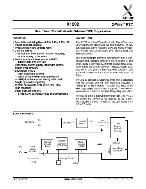
X12022-Wire™ RTC Real Time Clock/Calendar/Alarms/CPU SupervisorFEATURES•Selectable watchdog timer (0.25s, 0.75s, 1.75s, off)•Power on reset (250ms)•Programmable low voltage reset• 2 polled alarms—Settable on the second, minute, hour, day, month, or day of the week•2-wire interface interoperable with I2C—400kHz data transfer rate•Secondary power supply input with internal switch-over circuitry•Low power CMOS—<1µA operating current—<3mA active current during program—<400µA active current during data read •Single byte write capability•Typical nonvolatile write cycle time: 5ms•High reliability•Small package options—8-lead SOIC package, 8-lead TSSOP package DESCRIPTIONThe X1202 is a Real Time Clock with Clock/Calendar/ CPU Supervisor circuits and two polled alarms. The dual port clock and alarm registers allow the clock to oper-ate, without loss of accuracy, even during read and write operations.The clock/calendar provides functionality that is con-trollable and readable through a set of registers. The clock, using a low-cost 32.768kHz crystal input, accu-rately tracks the time in seconds, minutes, hours, date, day, month and years. It has leap year correction and automatic adjustment for months with less than 31 days.The X1202 provides a watchdog timer with 3 selectable time out periods and off. The watchdog activates a RESET pin when it expires. The reset also goes active when V CC drops below a fixed trip point. There are two alarms where a match is monitored by polling status bits. The device offers a backup power input pin. This V BACK pin allows the device to be backed up by a non-rechargeable battery. The RTC is fully operational from 1.8 to 5.5 volts.BLOCK DIAGRAMSCLSDA元器件交易网X1202PIN CONFIGURATIONPIN DESCRIPTIONSSerial Clock (SCL)The SCL input is used to clock all data into and out of the device. The input buffer on this pin is always active (not gated).Serial Data (SDA)SDA is a bidirectional pin used to transfer data into and out of the device. It has an open drain output and may be wire ORed with other open drain or open collector outputs. The input buffer is always active (not gated). An open drain output requires the use of a pull-up resistor. The output circuitry controls the fall time of the output signal with the use of a slope controlled pull-down. The circuit is designed for 400kHz 2-wire inter-face speeds.V BACKThis input provides a backup supply voltage to the device. V BACK supplies power to the device in the event the V CC supply fails.RESET Output—RESETThis is a reset signal output. This signal notifies a host processor that the watchdog time period has expired or that the supply voltage V CC has dropped below a fixed V TRIP threshold. It is an open drain active LOW output. X1, X2The X1 and X2 pins are the input and output,respectively, of an inverting amplifier that can be configured for use as an on-chip oscillator. A32.768kHz quartz crystal is used. Recommended crystalinput. The power control circuit will switch to V BACK when V CC < VBACK – 0.2V . It will switch back to V CC when V CC exceeds V BACK . Figure 2. Power ControlREAL TIME CLOCK OPERATIONThe Real Time Clock (RTC) uses an external,32.768kHz quartz crystal to maintain an accurate inter-nal representation of the year, month, day, date, hour,minute, and seconds. The RTC has leap-year correc-tion and century byte. The clock also corrects for months having fewer than 31 days and has a bit that controls 24-hour or AM/PM format. When the X1202powers up after the loss of both V CC and V BACK , the clock will not increment until at least one byte is written to the clock register.Reading the Real Time ClockThe RTC is read by initiating a Read command and specifying the address corresponding to the register of the real time clock. The RTC Registers can then be read in a Sequential Read Mode. Since the clock runs continuously and a read takes a finite amount of time,there is the possibility that the clock could change dur-ing the course of a read operation. In this device, the元器件交易网X1202time is latched by the read command (falling edge of the clock on the ACK bit prior to RTC data output) into a separate latch to avoid time changes during the read operation. The clock continues to run. Alarms occurring during a read are unaffected by the read operation. Writing to the Real Time ClockThe time and date may be set by writing to the RTC registers. T o avoid changing the current time by an uncompleted write operation, the current time value is loaded into a separate buffer at the falling edge of the clock on the ACK bit before the RTC data input bytes, the clock continues to run. The new serial input data replaces the values in the buffer. This new RTC value is loaded back into the RTC register by a stop bit at the end of a valid write sequence. An invalid write opera-tion aborts the time update procedure and the contents of the buffer are discarded. After a valid write operation the RTC will reflect the newly loaded data beginning with the first “one second” clock cycle after the stop bit. The RTC continues to update the time while an RTC register write is in progress and the RTC continues to run during any nonvolatile write sequences. A single byte may be written to the RTC without affecting the other bytes.CLOCK/CONTROL REGISTERS (CCR)The Control/Clock Registers are located in an area separate from the EEPROM array and are only acces-sible following a slave byte of “1101111x” and reads or writes to addresses [0000h:003Fh].CCR AccessThe contents of the CCR can be modified by perform-ing a byte or a page write operation directly to any address in the CCR. Prior to writing to the CCR (except the status register), however, the WE L and RWEL bits must be set using a two step process (See section “Writing to the Clock/Control Registers.”)The CCR is divided into 5 sections. These are:1. Alarm 0 (8 bytes)2. Alarm 1 (8 bytes)3. Control (1 byte)4. Real Time Clock (8 bytes)5. Status (1 byte)Sections 1) through 3) are nonvolatile and Sections 4) and 5) are volatile. E ach register is read and written through buffers. The nonvolatile portion (or the counter portion of the RTC) is updated only if RWEL is set and only after a valid write operation and stop bit. A sequential read or page write operation provides access to the contents of only one section of the CCR per operation. Access to another section requires a new operation. Continued reads or writes, once reach-ing the end of a section, will wrap around to the start of the section. A read or page write can begin at any address in the CCR.Section 5) is a volatile register. It is not necessary to set the RWE L bit prior to writing the status register. Section 5) supports a single byte read or write only. Continued reads or writes from this section terminates the operation.The state of the CCR can be read by performing a ran-dom read at any address in the CCR at any time. This returns the contents of that register location. Additional registers are read by performing a sequential read. The read instruction latches all clock registers into a buffer, so an update of the clock does not change the time being read. At the end of a read, the master supplies a stop condition to end the operation and free the bus. After a read of the CCR, the address remains at the previous address +1 so the user can execute a current address read of the CCR and continue reading the next Register.ALARM REGISTERSThere are two alarm registers whose contents mimic the contents of the RTC register, but add enable bits and exclude the 24-hour time selection bit. The enable bits specify which registers to use in the comparison between the Alarm and real time registers. For example:–The user can set the X1202 to alarm every Wednes-day at 8:00AM by setting the EDWn, the EHRn and EMNn enable bits to ‘1’ and setting the DWAn, HRAn and MNAn Alarm registers to 8:00AM Wednesday.–A daily alarm for 9:30PM results when the EHRn and EMNn enable bits are set to ‘1’ and the HRAn and MNAn registers set 9:30PM.–Setting the EMOn bit in combination with other enable bits and a specific alarm time, the user can establish an alarm that triggers at the same time once a year.When there is a match, an alarm flag is set. The occur-rence of an alarm can only be determined by polling the AL0 and AL1 bits.The alarm enable bits are located in the MSB of the particular register. When all enable bits are set to ‘0’, there are no alarms.元器件交易网X1202Table 1. Clock/Control Memory MapAddr.TypeRegNameBitRangeFactorySetting 76543210(optional)003F Status SR BAT AL1AL000RWEL WEL RTCF01h0037RTC(SRAM)Y2K00Y2K21Y2K20Y2K1300Y2K1019/2020h0036DW00000DY2DY1DY00-600h 0035YR Y23Y22Y21Y20Y13Y12Y11Y100-9900h 0034MO000G20G13G12G11G101-1200h 0033DT00D21D20D13D12D11D101-3100h 0032HR MIL0H21H20H13H12H11H100-2300h 0031MN0M22M21M20M13M12M11M100-5900h 0030SC0S22S21S20S13S12S11S100-5900h 0010Control(EEPROM)BL000WD1WD000000h000F Alarm1(EEPROM)Y2K000A1Y2K21A1Y2K20A1Y2K1300A1Y2K1019/2020h000E DWA0EDW10000DY2DY1DY00-600h 000D YRA0Unused - Default = RTC Year value000C MOA0EMO100A1G20A1G13A1G12A1G11A1G101-1200h 000B DTA0EDT10A1D21A1D20A1D13A1D12A1D11A1D101-3100h 000A HRA0EHR10A1H21A1H20A1H13A1H12A1H11A1H100-2300h 0009MNA0EMN1A1M22A1M21A1M20A1M13A1M12A1M11A1M100-5900h 0008SCA0ESC1A1S22A1S21A1S20A1S13A1S12A1S11A1S100-5900h0007Alarm0(EEPROM)Y2K100A0Y2K21A0Y2K20A0Y2K1300A0Y2K1019/2020h0006DWA1EDW00000DY2DY1DY00-600h 0005YRA1Unused - Default = RTC Year value0004MOA1EMO000A0G20A0G13A0G12A0G11A0G101-1200h 0003DTA1EDT00A0D21A0D20A0D13A0D12A0D11A0D101-3100h 0002HRA1EHR00A0H21A0H20A0H13A0H12A0H11A0H100-2300h 0001MNA1EMN0A0M22A0M21A0M20A0M13A0M12A0M11A0M100-5900h 0000SCA1ESC0A0S22A0S21A0S20A0S13A0S12A0S11A0S100-5900hREAL TIME CLOCK REGISTERSYear 2000 (Y2K)The X1202 has a century byte that “rolls over” from 19 to 20 when the years byte changes from 99 to 00. The Y2K byte can contain only the values of 19 or 20.Day of the Week Register (DW)This register provides a Day of the Week status and uses three bits DY2 to DY0 to represent the seven days of the week. The counter advances in the cycle 0-1-2-3-4-5-6-0-1-2-... The assignment of a numerical value to a specific day of the week is arbitrary and may be decided by the system software designer. The Clock Default values define 0 = Sunday.元器件交易网X1202Clock/Calendar Register (YR, MO, DT, HR, MN, SC) These registers depict BCD representations of the time. As such, SC (Seconds) and MN (Minutes) range from 0 to 59, HR (Hour) is 1 to 12 with an AM or PM indicator (H21 bit) or 0 to 23 (with MIL = 1), DT (Date) is 1 to 31, MO (Month) is 1 to 12, YR (Y ear) is 0 to 99.24 Hour TimeIf the MIL bit of the HR register is 1, the RTC uses a 24-hour format. If the MIL bit is 0, the RTC uses a 12-hour format and bit H21 functions as an AM/PM indica-tor with a ‘1’ representing PM. The clock defaults to Standard Time with H21 = 0.Leap YearsLeap years add the day February 29 and are defined as those years that are divisible by 4. Y ears divisible by 100 are not leap years, unless they are also divisible by 400. This means that the year 2000 is a leap year, the year 2100 is not. The X1202 does not correct for the leap year in the year 2100.STATUS REGISTER (SR)The Status Register is located in the RTC area at address 003Fh. This is a volatile register only and is used to control the WE L and RWE L write enable latches, read two power status and two alarm bits. This register is separate from both the array and the Clock/ Control Registers (CCR).Table 2. Status Register (SR)BAT: Battery Supply—VolatileThis bit set to “1” indicates that the device is operating from V BACK, not V CC. It is a read only bit and is set/ reset by hardware.AL1, AL0: Alarm bits—VolatileThese bits announce if either alarm 1 or alarm 2 match the real time clock. If there is a match, the respective bit is set to ‘1’. The falling edge of the last data bit in a SR Read operation resets the flags. Note: Only the AL bits that are set when an SR read starts will be reset. An alarm bit that is set by an alarm occurring during an SR read operation will remain set after the read operation is complete.RWEL: Register Write Enable Latch—VolatileThis bit is a volatile latch that powers up in the LOW (disabled) state. The RWEL bit must be set to “1” prior to any writes to the Clock/Control Registers. Writes to RWEL bit do not cause a nonvolatile write cycle, so the device is ready for the next operation immediately after the stop condition. A write to the CCR requires both the RWE L and WE L bits to be set in a specific sequence. RWEL bit is reset after each high voltage or reset by sending 00h to status register.WEL: Write Enable Latch—VolatileThe WEL bit controls the access to the CCR and mem-ory array during a write operation. This bit is a volatile latch that powers up in the LOW (disabled) state. While the WE L bit is LOW, writes to the CCR or any array address will be ignored (no acknowledge will be issued after the Data Byte). The WEL bit is set by writing a “1”to the WEL bit and zeroes to the other bits of the Status Register. Once set, WEL remains set until either reset to “0” (by writing a “0” to the WEL bit and zeroes to the other bits of the Status Register) or until the part pow-ers up again. Writes to WEL bit do not cause a nonvol-atile write cycle, so the device is ready for the next operation immediately after the stop condition.RTCF: Real Time Clock Fail Bit—VolatileThis bit is set to a ‘1’ after a total power failure. This is a read only bit that is set by hardware when the device powers up after having lost all power to the device. The bit is set regardless of whether V CC or V BACK is applied first. The loss of one or the other supplies does not result in setting the RTCF bit. The first valid write to the RTC (writing one byte is sufficient) resets the RTCF bit to ‘0’.Unused BitsThese devices do not use bits 3 or 4, but must have a zero in these bit positions. The Data Byte output during a SR read will contain zeros in these bit locations.CONTROL REGISTERWatchdog Timer Control BitsThe bits WD1 and WD0 control the period of the Watchdog Timer. See T able 3 for options.Addr76543210003Fh BAT AL1AL000RWEL WEL RTCFDefault00000001元器件交易网X1202Table 3. Watchdog Timer Time Out OptionsWRITING TO THE CLOCK/CONTROL REGISTERS Changing any of the nonvolatile bits of the clock/control register requires the following steps:–Write a 02H to the status register to set the Write Enable Latch (WEL). This is a volatile operation, so there is no delay after the write. (Operation pre-ceeded by a start and ended with a stop).–Write a 06H to the status register to set both the Register Write Enable Latch (RWEL) and the WEL bit. This is also a volatile cycle. The zeros in the data byte are required. (Operation preceeded by a start and ended with a stop).–Write one to 8 bytes to the clock/control registers with the desired clock, alarm, or control data. This sequence starts with a start bit, requires a slave byte of “11011110” and an address within the CCR and is terminated by a stop bit. A write to the CCR changes EEPROM values so these initiate a nonvolatile write cycle and will take up to 10ms to complete. Writes to undefined areas have no effect. The RWEL bit is reset by the completion of a nonvolatile write cycle, so the sequence must be repeated to again initiate another change to the CCR contents. If the sequence is not completed for any reason (by sending an incorrect number of bits or sending a start instead of a stop, for example) the RWEL bit is not reset and the device remains in an active mode.–The RWEL and WEL bits can be reset by writing a 0 to the status register.–A read operation occurring between any of the previous operations will not interrupt the register write operation. POWER ON RESETApplication of power to the X1202 activates a power on reset circuit that pulls the RESET pin active. This signal provides several benefits.–It prevents the system microprocessor from starting to operate with insufficient voltage.–It prevents the processor from operating prior to sta-bilization of the oscillator.–It allows time for an FPGA to download its configura-tion prior to initialization of the circuit.When V CC exceeds the device V TRIP threshold value for 250ms the circuit releases RE SE T, allowing the system to begin operation.WATCHDOG TIMER OPERATIONThe watchdog timer is selectable. By writing a value to WD1 and WD0, the watchdog timer can be set to 3 dif-ferent time out periods or off. When the watchdog timer is set to off, the watchdog circuit is configured for low power operation.Watchdog Timer RestartThe Watchdog Timer is restarted by a falling edge of SDA when the SCL line is high. This is also referred to as start condition. The restart signal restarts the watch-dog timer counter, resetting the period of the counter back to the maximum. If another start fails to be detected prior to the watchdog timer expiration, then the RE SE T pin becomes active. In the event that the restart signal occurs during a reset time out period, the restart will have no effect.LOW VOLTAGE RESET OPERATIONWhen a power failure occurs, and the voltage to the part drops below a fixed V TRIP voltage, a reset pulse is issued to the host microcontroller. The circuitry monitors the V CC line with a voltage comparator which senses a preset threshold voltage. Power up and power down waveforms are shown in Figure 4. The low voltage reset circuit is to be designed so the RE SE T signal is valid down to 1.0V.When the low voltage reset signal is active, the operation of any in-progress nonvolatile write cycle is unaffected, allowing a nonvolatile write to continue as long as possi-ble (down to the power on reset voltage). The low voltage reset signal, when active, terminates in-progress commu-nications to the device and prevents new commands, to reduce the likelihood of data corruption.WD1WD0Watchdog Time Out Period00 1.75 seconds01750 milliseconds10250 milliseconds11disabled元器件交易网X1202Figure 3. Watchdog Restart/Time OutFigure 4. Power On Reset and Low Voltage ResetV CC THRESHOLD RESET PROCEDUREThe X1202 is shipped with a standard V CC threshold (V TRIP) voltage. This value will not change over normal operating and storage conditions. However, in applica-tions where the standard V TRIP is not exactly right, or if higher precision is needed in the V TRIP value, the X1202 threshold may be adjusted. The procedure is described below, and uses the application of a nonvolatile write control signal.Setting the V TRIP VoltageThis procedure is used to set the V TRIP to a higher voltage value. It is necessary to reset the trip point before setting the new value.T o set the new V TRIP voltage, apply the desired V TRIP threshold voltage to the V CC pin and tie the RE SE T pad pin to the programming voltage V P. Then write data 00h to address 01h. The stop bit following a valid write operation initiates the V TRIP programming sequence. Bring RESET to V CC to complete the operation. Note: This operation also writes 00h to address 01h of the EEPROM array.元器件交易网Figure 5. Set V TRIP Level Sequence (V CC = desired V TRIP value)Resetting the V TRIP VoltageThis procedure is used to set the V TRIP to a “native”voltage level. For example, if the current V TRIP is 4.4V and the new V TRIP must be 4.0V , then the V TRIP must be reset. When V TRIP is reset, the new V TRIP is less than 1.7V . This procedure must be used to set the volt-age to a lower value.T o reset the new V TRIP voltage, apply more than 3V to the V CC pin and tie the RESET pin to the programming voltage V P . Then write 00h to address 03h. The stop bit of a valid write operation initiates the V TRIP programming sequence. Bring RESET to complete the operation. Note: This operation also writes 00h to address 03h of the EEPROM array.Figure 6. Reset V TRIP Level Sequence (V CC > 3V)Figure 7. Sample V TRIP Reset Circuit01234567SCLSDAAEh0123456703hRESET V P = 15V00h012345670123456700hV CCV CCSERIAL COMMUNICATIONInterface ConventionsThe device supports a bidirectional bus oriented proto-col. The protocol defines any device that sends data onto the bus as a transmitter, and the receiving device as the receiver. The device controlling the transfer is called the master and the device being controlled is called the slave. The master always initiates data transfers, and provides the clock for both transmit and receive operations. Therefore, the devices in this family operate as slaves in all applications.Clock and DataData states on the SDA line can change only during SCL LOW. SDA state changes during SCL HIGH are reserved for indicating start and stop conditions. See Figure 8.Figure 8. Valid Data Changes on the SDA BusStart ConditionAll commands are preceded by the start condition, which is a HIGH to LOW transition of SDA when SCL is HIGH. The device continuously monitors the SDA and SCL lines for the start condition and will not respond to any command until this condition has been met. See Figure 9.Stop ConditionAll communications must be terminated by a stop con-dition, which is a LOW to HIGH transition of SDA when SCL is HIGH. The stop condition is also used to place the device into the Standby power mode after a read sequence. A stop condition can only be issued after the transmitting device has released the bus. See Figure 8. AcknowledgeAcknowledge is a software convention used to indicate successful data transfer. The transmitting device, either master or slave, will release the bus after transmitting eight bits. During the ninth clock cycle, the receiver will pull the SDA line LOW to acknowledge that it received the eight bits of data. Refer to Figure 10.Figure 9. Valid Start and Stop ConditionsFigure 10. Acknowledge Response From ReceiverThe device will respond with an acknowledge after rec-ognition of a start condition and if the correct device identifier and select bits are contained in the slave address byte. If a write operation is selected, the device will respond with an acknowledge after the receipt of each subsequent eight bit word. The device will acknowledge all incoming data and address bytes, except for:–The slave address byte when the device identifier and/or select bits are incorrect–All data bytes of a write when the WEL in the write protect register is LOW–The 2nd data byte of a status register write operation (only 1 data byte is allowed)In the read mode, the device will transmit eight bits of data, release the SDA line, then monitor the line for an acknowledge. If an acknowledge is detected and no stop condition is generated by the master, the device will continue to transmit data. The device will terminate further data transmissions if an acknowledge is not detected. The master must then issue a stop condition to return the device to standby mode and place the device into a known state.WRITE OPERATIONSByte WriteFor a byte write operation, the device requires the slave address byte and the CCR address bytes. This gives the master access to any one of the words in the CCR. (Note: Prior to writing to the CCR, the master must write a 02h, then 06h to the status register in two preceeding operations to enable the write operation. See “Writing to the Clock/Control Registers” on page 6.) Upon receipt of each address byte, the X1202 responds with an acknowledge. After receiving both address bytes the X1202 awaits the eight bits of data. After receiving the 8 data bits, the X1202 again responds with an acknowledge. The master then termi-nates the transfer by generating a stop condition. The X1202 then begins an internal write cycle of the data to the nonvolatile memory. During the internal write cycle, the device inputs are disabled, so the device will not respond to any requests from the master. The SDA out-put is at high impedance. See Figure 11.Page WriteThe X1202 has a page write operation. It is initiated in the same manner as the byte write operation; but instead of terminating the write cycle after the first data byte is transferred, the master can transmit up to 7 more bytes to the clock/control registers.Note: Prior to writing to the CCR, the master must write a 02h, then 06h to the status register in two pre-ceeding operations to enable the write operation. See “Writing to the Clock/Control Registers” on page 6.)Figure 11. Byte Write SequenceFigure 12. Page Write SequenceS t a r tS t o pSlave AddressCCR Address 1 DataA C KA C KSDA Bus Signals from the SlaveSignals from the Master 0CCR Address 0111101100000000A C KA C KCCR Address 0S t a r tS t o pSlave AddressCCR Address 1Data (n)A C KA C KA C KSDA BusSignals from the SlaveSignals from the MasterData (1)A C K(1 ≤ n 64)111101100000000After the receipt of each byte, the X1202 responds with an acknowledge, and the address is internally incrimi-nated by one. When the counter reaches the end of the page, it “rolls over” and goes back to the first address on the same page. If the master supplies more than 8bytes of data, then the previously loaded data is over written by the new data, one byte at a time. The master terminates the data byte loading by issuing a stop con-dition, which causes the device to begin the non vola-tile write cycle. As with the byte write operation, all inputs are disabled until completion of the internal write cycle. Refer to Figure 12 for the address, acknowledge,and data transfer sequence.Stops and Write ModesStop conditions that terminate write operations must be sent by the master after sending at least 1 full data byte and its associated ACK signal. If a stop is issued in the middle of a data byte, or before 1 full data byte +ACK is sent, then the device will reset itself without performing the write. The contents of the array will not be affected.Acknowledge PollingThe disabling of the inputs during non volatile write cycles can be used to take advantage of the typical 5ms write cycle time. Once the stop condition is issued to indicate the end of the master’s byte load operation,the device initiates the internal non volatile write cycle.Acknowledge polling can be initiated immediately. T o do this, the master issues a start condition followed by the slave address byte for a write or read operation. If the device is still busy with the non volatile write cycle then no ACK will be returned. If the device has com-pleted the write operation, an ACK will be returned and the host can then proceed with the read or write opera-tion. Refer to the flow chart in Figure 13.Figure 13. Acknowledge Polling SequenceREAD OPERATIONSThere are three basic read operations: Current Address Read, Random Read, and Sequential Read.Current Address ReadInternally the device contains an address counter that maintains the address of the last word read incrimi-nated by one. Therefore, if the last read was to address n, the next read operation would access data from address n + 1.Upon receipt of the slave address byte with the R/W bit set to one, the device issues an acknowledge and then transmits the eight bits of the data byte. The master terminates the read operation when it does not respond with an acknowledge during the ninth clock and then issues a stop condition. Refer to Figure 14 for the address, acknowledge, and data transfer sequence.It should be noted that the ninth clock cycle of the read operation is not a “don’t care.” T o terminate a read operation, the master must either issue a stop condi-tion during the ninth cycle or hold SDA HIGH during the ninth clock cycle and then issue a stop condition.Figure 14. Current Address Read SequenceS t a r tS t o pSlave AddressDataA C KSDA Bus Signals from the SlaveSignals from the Master 11111011。
MAXIM MAX3570 MAX3571 MAX3573 说明书

_________________________________概述MAX3570/MAX3571/MAX3573低成本、宽带、两次变频调谐器芯片设计用于数字电视接收机。
每款芯片集成了所有必需的射频功能模块,其中包括一个集成的高中频滤波器、全集成VCO、中频VGA。
工作频率范围从50MHz 至878MHz,同时提供超过60dB的RF及IF可控增益范围。
MAX3570/MAX3571具有以44MHz为中心的中频频率,而MAX3573具有以36MHz为中心的中频输出。
这三款芯片都包括了可变增益射频前端,噪声系数仅为8dB。
双频合成器产生两个本振(LO)频率,提供优异的相位噪声性能,在10kHz频偏时相位噪声为-86dBc/Hz。
集成的高中频(HI-IF)滤波器有55dBc (典型值)的镜像抑制。
仅需要一个中频SAW滤波器、无源环路滤波器和晶体振荡器即可构建完整的单芯片调谐器。
MAX3570芯片编程和配置由3线串行接口完成,而MAX3571/MAX3573芯片编程和配置由2线串行接口完成。
MAX3570/MAX3571/MAX3573采用48引脚QFN-EP封装,可工作于商业温度范围(0°C 至+70°C)。
_________________________________应用DVB-C数字电视接收机ATSC数字电视接收机有线电视调制解调器DOCSIS/EURO DOCSIS调制解调器ITU J.83数字机顶盒___________________________________特性♦全集成HI-IF滤波器♦全集成VCO,无需外部元器件和走线。
♦8dB低噪声系数♦高线性—大于54dBc, CSO, CTB, X-MOD。
♦业界最小的封装♦优异的相位噪声,可用于256-QAM、8-VSB和COFDM。
MAX3570/MAX3571/MAX3573高中频(HI-IF)单片宽带调谐器________________________________________________________________Maxim Integrated Products1_____________________引脚排列和功能框图______________________________定购信息*EP = 裸露焊盘。
A1203中文资料

A1203中⽂资料Continuous-time operation – Fast power-on time– Low noiseStable operation over full operating temperature range Reverse battery protectionSolid-state reliabilityFactory-programmed at end-of-line for optimum performance Robust EMC performance High ESD ratingRegulator stability without a bypass capacitorA1201, A1202, A1203 and A1204 Hall-effect bipolar switches are . The extensive on-board protection circuitry makes Continuous-Time Bipolar Switch FamilyFunctional Block DiagramVOUTTerminal ListName DescriptionNumberPackage LH Package UAVCC Connects power supply to chip 11VOUT Output from circuit 23GNDGround32Part Number Packing*MountingAmbient, T A B RP (Min)B OP (Max)A1201ELHLT-T 7-in. reel, 3000 pieces/reel 3-pin SOT23W surface mount –40oC to 85oC–5050A1201EUA-T Bulk, 500 pieces/bag 3-pin SIP through hole A1201LLHLT-T 7-in. reel, 3000 pieces/reel 3-pin SOT23W surface mount –40oC to 150oC A1201LUA-T Bulk, 500 pieces/bag 3-pin SIP through hole A1202ELHLT-T 7-in. reel, 3000 pieces/reel 3-pin SOT23W surface mount –40oC to 85oC–7575A1202EUA-T Bulk, 500 pieces/bag 3-pin SIP through hole A1202LLHLT-T 7-in. reel, 3000 pieces/reel 3-pin SOT23W surface mount –40oC to 150oC A1202LUA-T Bulk, 500 pieces/bag 3-pin SIP through hole A1203ELHLT-T 7-in. reel, 3000 pieces/reel 3-pin SOT23W surface mount –40oC to 85oC–9595A1203EUA-T Bulk, 500 pieces/bag 3-pin SIP through hole A1203LLHLT-T 7-in. reel, 3000 pieces/reel 3-pin SOT23W surface mount –40oC to 150oC A1203LUA-T Bulk, 500 pieces/bag 3-pin SIP through hole A1204ELHLT-T 7-in. reel, 3000 pieces/reel 3-pin SOT23W surface mount –40oC to 85oC–150150A1204EUA-T Bulk, 500 pieces/bag 3-pin SIP through hole A1204LLHLT-T 7-in. reel, 3000 pieces/reel 3-pin SOT23W surface mount –40oC to 150oCA1204LUA-TBulk, 500 pieces/bag3-pin SIP through hole*Contact Allegro for additional packing options.Product Selection GuideOPERATING CHARACTERISTICS over full operating voltage and ambient temperature ranges, unless otherwise noted Characteristic Symbol Test Conditions Min.Typ.Max.Units Electrical CharacteristicsSupply Voltage1V CC Operating, T J < 165°C 3.8–24V Output Leakage Current I OUTOFF V OUT = 24 V, B < B RP––10µA Output On Voltage V OUT(SAT)I OUT = 20 mA, B > B OP–215400mVPower-On Time2t PO Slew rate (dV CC/dt) < 2.5 V/µs, B > B OP + 5 G orB < B RP – 5 G––4µsOutput Rise Time3t r V CC = 12 V, R LOAD = 820 ?, C S = 12 pF––2µs Output Fall Time3t f V CC = 12 V, R LOAD = 820 ?, C S = 12 pF––2µsSupply Current I CCON B > B OP– 3.87.5mA I CCOFF B < B RP– 3.57.5mAReverse Battery Current I RCC V RCC = –30 V–––10mA Supply Zener Clamp Voltage V Z I CC = 10.5 mA; T A = 25°C32––V Supply Zener Current4I Z V Z = 32 V; T A = 25°C––10.5mA Magnetic Characteristics5Operate Point B OP A1201South pole adjacent to branded faceof device–401550G A1202–2675G A1203–2695G A1204–10042150GRelease Point B RP A1201North pole adjacent to branded faceof device–50–1540G A1202–75–26–G A1203–95–26–G A1204–150–40100GHysteresis B HYS A1201B OP – B RP53055G A12023052–G A12033052–G A12045082115G1 Maximum voltage must be adjusted for power dissipation and junction temperature, see Power Derating section.2 For V CC slew rates greater than 250 V/µs, and T A = 150°C, the Power-On Time can reach its maximum value.3 C S =oscilloscope probe capacitance.4 Maximum current limit is equal to the maximum I CC(max) + 22 mA.5 Magnetic flux density, B, is indicated as a negative value for north-polarity magnetic fields, and as a positive value for south-polarity magnetic fields. This so-called algebraic convention supports arithmetic comparison of north and south polarity values, where the relative strength of the field is indicated by the absolute value of B, and the sign indicates the polarity of the field (for example, a –100 G field and a 100 G field have equivalent strength, but opposite polarity).DEVICE QUALIFICATION PROGRAMContact Allegro for information.EMC (Electromagnetic Compatibility) REQUIREMENTSContact Allegro for information.THERMAL CHARACTERISTICS may require derating at maximum conditions, see application information CharacteristicSymbolTest ConditionsValue Units Package Thermal ResistanceR θJAPackage LH, minimum-K PCB (single layer, single-sided with copper limited to solder pads)110oC/W Package LH, low-K PCB (single layer, double-sided with 0.926 in 2 copper area)228oC/W Package UA, minimum-K PCB (single layer, single-sided with copper limited to solder pads)165oC/W678923451011121314151617181920212223242520406080100120140160180M a x i m u m A l l o w a b l e V C C (V )T=165oC;I =I Power Derating Curve V CC(min)V CC(max)100200300400500600700800900100011001200130014001500160017001800190020406080100120140160180Temperature (°C)P o w e r D i s s i p a t i o n ,P D (m W )Power Dissipation versus Ambient TemperatureCharacteristic DataFunctional DescriptionBipolar Device SwitchingThe devices of the A120X family provide highly sensitive switching for applications using magnetic fields of alternating polarities, such as ring magnets. There are three switching modes for bipolar devices, referred to as latch , unipolar switch , and negative switch . Mode is determined by the switchpoint charac-teristics of the individual device. The characteristic hysteresis, B HYS , of the device, is the difference in the relative magnetic strength and polarity of the switchpoints of the device. (Note that, in the following descriptions, a negative magnetic value indicates a north polarity field, and a positive magnetic value indicates a south polarity field. For a given value of magnetic strength, B X , the values –B X and B X indicate two fields of equal strength, but opposite polarity. B = 0 indicates the absence of a magnetic field.)Bipolar devices typically behave as latches. In this mode, magnetic fields of opposite polarity and equivalent strengths are needed to switch the output. When the magnetic fields are removed (B → 0) the device remains in the same state until a magnetic field of the opposite polarity and of sufficient strength causes it to switch. The hysteresis of latch mode behavior isshown in panel A of figure 1.In contrast to latching, when a device exhibits unipolar switch-ing, it only responds to a south magnetic field. The field must be of sufficient strength, > B OP , for the device to operate. When the field is reduced beyond the B RP level, the device switches back to the high state, as shown in panel B of figure 1. Devices exhibiting negative switch behavior operate in a similar but opposite manner. A north polarity field of sufficient strength, > B RP , (more north than B RP ) is required for operation, although the result is that V OUT switches high, as shown in panel C. WhenFigure 1. Bipolar Device Output Switching Modes. These behaviors can be exhibited when using a circuit such as that shown in panel D. Panel A displays the hysteresis when a device exhibits latch mode (note that the B HYS band incorporates B= 0), panel B shows unipolar switch behavior (the B HYS band is more positive than B = 0), and panel C shows negative switch behavior (the B HYS band is more negative than B = 0). Bipolar devices, such as the 120x family, can operate in any of the three modes.HYS V O U THYS HYSV OUT(SAT)CC(A)(B)(C)(D)the field is reduced beyond the B OP level, the device switches back to the low state.The typical output behavior of the A120x devices is latching. That is, switching to the low state when the magnetic field at the Hall sensor exceeds the operate point threshold, B OP . At this point, the output voltage is V OUT(SAT). When the magnetic field is reduced to below the release point threshold, B RP , the device output, V OUT , goes high. The values of the magnetic parameters are specified in the Magnetic Characteristics table, on page 3. Note that, as shown in figure 1, these switchpoints can lie in either north or south polarity ranges.The A120x family is designed to attain a small hysteresis, and thereby provide more sensitive switching. Although this means that true latching behavior cannot be guaranteed in all cases, proper switching can be ensured by use of both south and north magnetic fields, as in a ring magnet. The hysteresis of the A120x family allows clean switching of the output, even in the presence of external mechanical vibration and electrical noise.Bipolar devices adopt an indeterminate output state when pow-ered-on in the absence of a magnetic field or in a field that lies within the hysteresis band of the device.For more information on Bipolar switches, refer to Application Note 27705, Understanding Bipolar Hall Effect Sensors . CONTINUOUS-TIME BENEFITSContinuous-time devices, such as the A120x family, offer the fastest available power-on settling time and frequency response. Due to offsets generated during the IC packaging process, continuous-time devices typically require programming after packaging to tighten magnetic parameter distributions. In con-trast, chopper-stabilized switches employ an offset cancellation technique on the chip that eliminates these offsets without the need for after-packaging programming. The tradeoff is a longer settling time and reduced frequency response as a result of the chopper-stabilization offset cancellation algorithm.Figure 2. Continuous-Time Application, B < B RP .. This figure illustrates the use of a quick cycle for chopping V CC in order to conserve battery power. Position 1, power is applied to the device. Position 2, the output assumes the correct state at a time prior to the maximum Power-On Time, t PO(max). The case shown is where the correct output state is HIGH . Position 3, t PO(max) has elapsed. The device output is valid. Position 4, after the output is valid, a control unit reads the output. Position5, power is removed from the device.VV PO(max)The choice between continuous-time and chopper-stabilized designs is solely determined by the application. Battery manage-ment is an example where continuous-time is often required. In these applications, V CC is chopped with a very small duty cycle in order to conserve power (refer to figure 4). The duty cycleis controlled by the power-on time, t PO, of the device. Because continuous-time devices have the shorter power-on time, they are the clear choice for such applications.For more information on the chopper stabilization technique, refer to Technical Paper STP 97-10, Monolithic Magnetic Hall Sensor Using Dynamic Quadrature Offset Cancellation and Technical Paper STP 99-1, Chopper-Stabilized Amplifiers with a Track-and-Hold Signal Demodulator.ADDITIONAL APPLICATIONS INFORMATION Extensive applications information for Hall-effect sensors is available in:Hall-Effect IC Applications Guide, Application Note 27701 Hall-Effect Devices: Gluing, Potting, Encapsulating, Lead Welding and Lead Forming, Application Note 27703.1Soldering Methods for Allegro’s Products – SMT and Through-Hole, Application Note 26009All are provided in Allegro Electronic Data Book, AMS-702, and the Allegro Web site,/doc/407cd0b7c77da26925c5b0c1.html .Power Derating Power DeratingThe device must be operated below the maximum junction temperature of the device, T J(max). Under certain combinations of peak conditions, reliable operation may require derating sup-plied power or improving the heat dissipation properties of the application. This section presents a procedure for correlating factors affecting operating T J. (Thermal data is also available on the Allegro MicroSystems Web site.)The Package Thermal Resistance, RθJA, is a figure of merit sum-marizing the ability of the application and the device to dissipate heat from the junction (die), through all paths to the ambient air. Its primary component is the Effective Thermal Conductivity, K, of the printed circuit board, including adjacent devices and traces. Radiation from the die through the device case, RθJC, is relatively small component of RθJA. Ambient air temperature,T A, and air motion are significant external factors, damped by overmolding.The effect of varying power levels (Power Dissipation, P D), can be estimated. The following formulas represent the fundamental relationships used to estimate T J, at P D.P D = V IN× I IN (1)T = P D× RθJA(2)T J = T A + ?T (3)For example, given common conditions such as: T A= 25°C,V CC = 12 V, I CC = 4 mA, and RθJA = 140 °C/W, then:P D = V CC× I CC = 12 V × 4 mA = 48 mWT = P D× RθJA = 48 mW × 140 °C/W = 7°CT J = T A + ?T = 25°C + 7°C = 32°CA worst-case estimate, P D(max), represents the maximum allow-able power level (V CC(max), I CC(max)), without exceeding T J(max), at a selected RθJA and T A.Example: Reliability for V CC at T A =150°C, package UA, using minimum-K PCB.Observe the worst-case ratings for the device, specifically:RθJA =165°C/W, T J(max) =165°C, V CC(max) =24 V, andI CC(max) =7.5mA.Calculate the maximum allowable power level, P D(max). First, invert equation 3:T max = T J(max) – T A = 165°C–150°C = 15°CThis provides the allowable increase to T J resulting from internal power dissipation. Then, invert equation 2:P D(max) = ?T max ÷ RθJA = 15°C ÷ 165 °C/W = 91 mWFinally, invert equation 1 with respect to voltage:V CC(est) = P D(max) ÷ I CC(max) =91 mW ÷ 7.5 mA = 12.1 VThe result indicates that, at T A, the application and device can dissipate adequate amounts of heat at voltages ≤V CC(est). Compare V CC(est) to V CC(max). If V CC(est)≤ V CC(max), then reli-able operation between V CC(est) and V CC(max) requires enhanced RθJA. If V CC(est)≥ V CC(max), then operation between V CC(est) and V CC(max) is reliable under these conditions.Package LH, 3-Pin (SOT-23W)Package UA, 3-PinThe products described herein are manufactured under one or more of the following U.S. patents: 5,045,920; 5,264,783; 5,442,283; 5,389,889; 5,581,179; 5,517,112; 5,619,137; 5,621,319; 5,650,719; 5,686,894; 5,694,038; 5,729,130; 5,917,320; and other patents pending.Allegro MicroSystems, Inc. reserves the right to make, from time to time, such de p ar t ures from the detail spec i f i c a t ions as may be required to permit improvements in the per f or m ance, reliability, or manufactur-ability of its products. Before placing an order, the user is cautioned to verify that the information being relied upon is current.Allegro products are not authorized for use as critical components in life-support devices or sys t ems without express written approval.The in f or m a t ion in c lud e d herein is believed to be ac c u r ate and reliable. How e v e r, Allegro MicroSystems, Inc. assumes no re s pon s i b il i t y for its use; nor for any in f ringe m ent of patents or other rights of third parties which may result from its use.Copyright ? 2005, Allegro MicroSystems, Inc.。
NCA-前言

ASME锅炉及压力容器规范国际性规范III 核设施部件建造规则ACI标准359-95美国国家标准NCA分卷第1册和第2册的总要求2004版2004年7月1日ASME锅炉及压力容器委员会核动力分委员会编著上海发电设备成套设计研究院翻译上海核工程研究设计院上海科学技术文献出版社出版日期:2004年7月1日(包括2003年7月及以前的各次增补)本国际规范或标准是按照符合美国国家标准准则的认可程序制定的,它是美国国家标准。
批准本规范或标准的“标准委员会”所组成经过协调,可保证技术权威和利益相关部门的人士都有机会参加。
规范或标准草案经过公开征求意见和公开评议,使产业界、学术界、监督机构和公众得以提出补充意见。
美国机械工程师学会(ASME)不对任何物项、建造、专利的装置或活动进行“批准”、“定等级”或“担保”。
ASME对与本文件述及的任何项目有联系的任何专利权的有效性,不作任何表态;不保证任何人在使用某一标准时是否违反法律侵犯有关专利证书,也不承担此类责任。
ASME明确告知规范或标准的使用人:确定任何这类专利权是否有效以及侵犯专利带来的风险,完全由他们自己负责。
不可把产业界人士或联邦政府代表的参与理解为产业界或联邦政府对本规范或标准的认可。
ASME只对那些按照ASME管理程序和方针发布的文件的“条款解释”负责,不允许以个人名义发布“条款解释”。
本文件中的“脚注”也是美国国家标准的组成部分。
ASME会员标志以上ASME标志是在美国专利局注册的。
“ASME”是美国机械工程师学会的商标。
凡事先未取得出版商书面认可,本文件的任一部分都不得以任何形式,包括电子检索系统或别的方式复制。
美国国会图书馆目录卡号:56-3934本规范英文原版在美国印刷美国机械工程师学会理事会于1914年通过本规范历次修订版本如下:1940,1941,1943,1946,1949,1952,1953,1956,1959,1962,1965,1968,1971,1974,1977,1980,1983,1986,1989,1992,1995,1998,2001,2004美国机械工程师学会地址:Three Park Avenue, New York, NY 10016-59902004版的版权归美国机械工程学会所有版权所有不得翻印2004版ASME锅炉及压力容器规范各卷名称(Sections)第Ⅰ卷动力锅炉建造规则第Ⅱ卷材料A篇—铁基材料技术规格B篇—非铁基材料技术规格C篇—焊条、焊丝及填充金属材料技术规格D篇—性能(美国通用单位)D篇—性能(国际单位)第Ⅲ卷NCA分卷—第1册和第2册的总要求第Ⅲ卷第1册NB分卷—1级部件NC分卷—2级部件ND分卷—3级部件NE分卷—MC级部件NF分卷—支承件NG分卷—堆芯支承结构NH分卷—高温使用的1级部件附录第Ⅲ卷第2册—混凝土安全壳规范第Ⅲ卷第3册—用于运输与储存乏燃料和高放射性材料及废料的安全容器第Ⅳ卷采暖锅炉建造规则第Ⅴ卷无损检测第Ⅵ卷采暖锅炉维护和运行推荐规则第Ⅶ卷动力锅炉维护推荐指南第Ⅷ卷压力容器建造规则第1册第2册—另一规则第3册—高压容器建造规则第Ⅸ卷焊接和钎焊评定第Ⅹ卷纤维增强塑料压力容器第Ⅺ卷核电厂部件在役检查规则第Ⅻ卷运输罐建造和持续使用规则增补(Addenda)本规范各卷每年出版包括补充和修改的彩页增补,将及时寄给有关卷的订户,直到2007版规范出版时为止。
DAC1210中文资料

TL H 5690MICRO-DAC DAC1208 DAC1209 DAC1210 DAC1230 DAC1231 DAC123212-Bit m P Compatible Double-Buffered D to A ConvertersFebruary1995 MICRO-DAC TM DAC1208 DAC1209 DAC1210 DAC1230 DAC1231 DAC123212-Bit m P CompatibleDouble-Buffered D to A ConvertersGeneral DescriptionThe DAC1208and the DAC1230series are12-bit multiply-ing D to A converters designed to interface directly with awide variety of microprocessors(8080 8048 8085 Z-80etc ) Double buffering input registers and associated con-trol lines allow these DACs to appear as a two-byte‘‘stack’’in the system’s memory or I O space with no additional in-terfacing logic requiredThe DAC1208series provides all12input lines to allow sin-gle buffering for maximum throughput when used with16-bitprocessors These input lines can also be externally config-ured to permit an8-bit data interface The DAC1230seriescan be used with an8-bit data bus directly as it internallyformulates the12-bit DAC data from its8input lines All ofthese DACs accept left-justified data from the processorThe analog section is a precision silicon-chromium(Si-Cr)R-2R ladder network and twelve CMOS current switchesAn inverted R-2R ladder structure is used with the binaryweighted currents switched between the I OUT1and I OUT2maintaining a constant current in each ladder leg indepen-dent of the switch state Special circuitry provides TTL logicinput voltage level compatibilityThe DAC1208series and DAC1230series are the12-bitmembers of a family of microprocessor compatible DACs(MICRO-DACs TM) For applications requiring other resolu-tions the DAC1000series for10-bit and DAC0830seriesfor8-bit are available alternativesFeaturesY Linearity specified with zero and full-scale adjust onlyY Direct interface to all popular microprocessorsY Double-buffered single-buffered or flow through digitaldata inputsY Logic inputs which meet TTL voltage level specs(1 4Vlogic threshold)Y Works with g10V reference full4-quadrantmultiplicationY Operates stand-alone(without m P)if desiredY All parts guaranteed12-bit monotonicY DAC1230series is pin compatible with the DAC0830series8-bit MICRO-DACsKey SpecificationsY Current Settling Time1m sY Resolution12BitsY Linearity(Guaranteedover temperature)10 11 or12Bits of FSY Gain Tempco1 3ppm CY Low Power Dissipation20mWY Single Power Supply5V DC to15V DC Typical ApplicationTL H 5690–1TRI-STATE is a registered trademark of National Semiconductor CorpMICRO-DAC TM is a trademark of National Semiconductor CorpC1995National Semiconductor Corporation RRD-B30M115 Printed in U S AAbsolute Maximum RatingsIf Military Aerospace specified devices are required please contact the National Semiconductor Sales Office Distributors for availability and specifications (Notes 1and 2)Supply Voltage (V CC )17V DC Voltage at Any Digital Input V CC to GNDVoltage at V REF Inputg 25VStorage Temperature Rangeb 65 C to a 150 CPackage Dissipation at T A e 25 C 500mW(Note 3)DC Voltage Applied to I OUT1or I OUT2(Note 4)b 100mV to V CCESD Susceptability800VOperating ConditionsLead Temperature (Soldering 10sec )300 CTemperature RangeT MIN s T A s T MAXDAC1208LCJ DAC1209LCJ DAC1210LCJ DAC1230LCJ DAC1231LCJ DAC1232LCJDAC1231LIN DAC1232LINb 40 C s T A s a 85 C DAC1208LCJ-1 DAC1210LCJ-1 DAC1230LCJ-1 DAC1231LCJ-1 DAC1232LCJ-1 DAC1231LCN DAC1232LCN DAC1231LCWM DAC1232LCWM 0 C s T A s a 70 C Range of V CC 4 75V DC to 16V DC Voltage at Any Digital InputV CC to GNDElectrical CharacteristicsV REF e 10 000V DC V CC e 11 4V DC to 15 75V DC unless otherwise noted Boldface limits apply from T MIN to T MAX (seeNote 13) all other limits T A e T J e 25 CTyp Tested Design ParameterConditions Notes(Note 10)Limit Limit Units (Note 5)(Note 6)Resolution121212BitsLinearity ErrorZero and Full-Scale 4 7 13(End Point Linearity)AdjustedDAC1208 DAC1230g 0 018g 0 018%of FSR DAC1209 DAC1231g 0 024g 0 024%of FSR DAC1210 DAC1232g 0 050g 0 05%of FSRDifferential Non-Linearity Zero and Full-Scale 4 7 13AdjustedDAC1208 DAC1230g 0 018g 0 018%of FSR DAC1209 DAC1231g 0 024g 0 024%of FSR DAC1210 DAC1232g 0 050g 0 05%of FSR Monotonicity 4121212Bits Gain Error (Min)Using Internal R Fb 7b 0 10 0%of FSR Gain Error (Max)V ref e g 10V g 1V7b 0 1b 0 2%of FSRGain Error Tempco 7g 1 3g 6 0ppm of FS C Power Supply RejectionAll Digital Inputs 7g 3 0g 30ppm of FSR VLatched HighReference Input Resistance (Min)13151010k X Reference Input Resistance (Max)152020Output Feedthrough ErrorV REF e 20Vp-p f e 100kHz All Data Inputs Latched 93 0mVp-pLowOutput CapacitanceAll Data Inputs I OUT1200pF Latched High I OUT270pF All Data Inputs I OUT170pF Latched LowI OUT2200pF Supply Current Drain 132 02 5mA Output Leakage Current I OUT1All Data Inputs Latched 11 130 11515nA LowI OUT2All Data Inputs Latched 11 130 11515nA HighDigital Input Threshold Low Threshold 130 80 8V DC High Threshold 132 22 2V DC Digital Input CurrentsDigital Inputs k 0 8V 13b 200b 200m A DC Digital Inputs l 2 2V131010m A DC2Electrical Characteristics(Continued)V REF e10 000V DC V CC e11 4V DC to15 75V DC unless otherwise noted Boldface limits apply from T MIN to T MAX(see Note13) all other limits T A e T J e25 CSee Typ Tested DesignSymbol Parameter ConditionsNote(Note10)Limit Limit Units (Note5)(Note6)AC CHARACTERISTICSt s Current Setting Time V IL e0V V IH e5V1 0m st W Write and XFER V IL e0V V IH e5V850320Pulse Width Min 320t DS Data Setup Time Min V IL e0V V IH e5V70320320t DH Data Hold Time Min V IL e0V V IH e5V3090ns90t CS Control Setup Time Min V IL e0V V IH e5V60320320t CH Control Hold Time Min V IL e0V V IH e5V010Note1 Absolute Maximum Ratings indicate limits beyond which damage to the device may occur DC and AC electrical specifications do not apply when operating the device beyond its specified operating conditionsNote2 All voltages are measured with respect to GND unless otherwise specifiedNote3 This500mW specification applies for all packages The low intrinsic power dissipation of this part(and the fact that there is no way to significantly modify the power dissipation)removes concern for heat sinkingNote4 Both I OUT1and I OUT2must go to ground or the virtual ground of an operational amplifier The linearity error is degraded by approximately V OS d V REF For example if V REF e10V then a1mV offset V OS on I OUT1or I OUT2will introduce an additional0 01%linearity errorNote5 Tested and guaranteed to National’s AOQL(Average Outgoing Quality Level)Note6 Design limits are guaranteed but not100%tested These limits are not used to calculate outgoing quality levels Guaranteed for V CC e11 4V to15 75V and V REF e b10V to a10VNote7 The unit FSR stands for full-scale range Linearity Error and Power Supply Rejection specs are based on this unit to eliminate dependence on a particular V REF value to indicate the true performance of the part The Linearity Error specification of the DAC1208is0 012%of FSR(max) This guarantees that after performing a zero and full-scale adjustment the plot of the4096analog voltage outputs will each be within0 012%c V REF of a straight line which passes through zero and full-scale The unit ppm of FSR(parts per million of full-scale range)and ppm of FS(parts per million of full-scale)are used for convenience to define specs of very small percentage values typical of higher accuracy converters In this instance 1ppm of FSR e V REF 106is the conversion factor to provide an actual output voltage quantity For example the gain error tempco spec of g6ppm of FS C represents a worst-case full-scale gain error change with temperature from b40 C to a85 C of g(6)(V REF 106)(125 C)or g0 75(10b3)V REF which is g0 075%of V REFNote8 This spec implies that all parts are guaranteed to operate with a write pulse or transfer pulse width(t W)of320ns A typical part will operate with t W of only 100ns The entire write pulse must occur within the valid data interval for the specified t W t DS t DH and t S to applyNote9 To achieve this low feedthrough in the D package the user must ground the metal lid If the lid is left floating the feedthrough is typically6mVNote10 Typicals are at25 C and represent the most likely parametric normNote11 A10nA leakage current with R Fb e20k and V REF e10V corresponds to a zero error of(10c10b9c20c103)c100%10V or0 002%of FSNote12 Human body model 100pF discharged through a1 5k X resistorNote13 Tested limit for b1suffix parts applies only at25 CConnection DiagramsDual-In-Line Package Dual-In-Line PackageTL H 5690–2See Ordering Information3Switching WaveformsTL H 5690–3Typical Performance CharacteristicsDigital Input Threshold vs V CCDigital Input Threshold vs TemperatureGain and Linearity Error Variation vs TemperatureGain and Linearity Error Variation vs Supply VoltageControl Set-Up Time t CS Data Hold Time t DHWrite Pulse Width t W Data Set-Up Time t DSTL H 5690–44Definition of Package Pinouts CONTROL SIGNALS(all control signals are level actuated) CS Chip Select(active low) The CS will enable WR1WR1 Write1 The active low WR1is used to load the digital data bits(DI)into the input latch The data in the input latch is latched when WR1is high The12-bit input latch is split into two latches One holds the first8bits while the other holds4bits The Byte1 Byte2control pin is used to select both latches when Byte1 Byte2is high or to overwrite the 4-bit input latch when in the low stateByte1 Byte2 Byte Sequence Control When this control is high all12locations of the input latch are enabled When low only the four least significant locations of the input latch are enabledWR2 Write2(active low) The WR2will enable XFER XFER Transfer Control Signal(active low) This signal in combination with WR2 causes the12-bit data which is available in the input latches to transfer to the DAC register DI0to DI11 Digital Inputs DI0is the least significant digital input(LSB)and DI11is the most significant digital input (MSB)I OUT1 DAC Current Output1 I OUT1is a maximum for a digital code of all1s in the DAC register and is zero for all 0s in the DAC registerI OUT2 DAC Current Output2 I OUT2is a constant minus I OUT1 or I OUT1a I OUT2e constant(for a fixed reference voltage) This constant current isV REF c 1b14096Jdivided by the reference input resistanceR Fb Feedback Resistor The feedback resistor is provided on the IC chip for use as the shunt feedback resistor for the external op amp which is used to provide an output voltage for the DAC This on-chip resistor should always be used (not an external resistor)since it matches the resistors in the on-chip R-2R ladder and tracks these resistors over temperatureV REF Reference Voltage Input This input connects an ex-ternal precision voltage source to the internal R-2R ladder V REF can be selected over the range of10V to b10V This is also the analog voltage input for a4-quadrant multiplying DAC applicationV CC Digital Supply Voltage This is the power supply pin for the part V CC can be from5V DC to15V DC Operation is optimum for15V DCGND Pins3and12of the DAC1208 DAC1209 and DAC1210must be connected to ground Pins3and10of the DAC1230 DAC1231 and DAC1232must be connectedto ground It is important that I OUT1and I OUT2are at ground potential for current switching applications Any difference of potential(V OS on these pins)will result in a linearity change ofV OS3V REFFor example if V REF e10V and these ground pins are9mV offset from I OUT1and I OUT2the linearity change will be 0 03%Definition of TermsResolution Resolution is defined as the reciprocal of the number of discrete steps in the DAC output It is directly related to the number of switches or bits within the DAC For example the DAC1208has212or4096steps and therefore has12-bit resolutionLinearity Error Linearity error is the maximum deviation from a straight line passing through the endpoints of the DAC transfer characteristic It is measured after adjusting for zero and full-scale Linearity error is a parameter intrinsic to the device and cannot be externally adjusted National’s linearity test(a)and the best straight line test(b) used by other suppliers are illustrated below The best straight line(b)requires a special zero and FS adjustment for each part which is almost impossible for the user to determine The end point test uses a standard zero FS ad-justment procedure and is a much more stringent test for DAC linearityPower Supply Sensitivity Power supply sensitivity is a measure of the effect of power supply changes on the DAC full-scale outputSettling Time Full-scale current settling time requires zero to full-scale or full-scale to zero output change Settling time is the time required from a code transition until the DAC output reaches within g LSB of the final output value Full-Scale Error Full-scale error is a measure of the output error between an ideal DAC and the actual device output Ideally for the DAC1208or DAC1230series full-scale is V REF b1LSB For V REF e10V and unipolar operation V FULL-SCALE e10 0000V b2 44mV e9 9976V Full-scale error is adjustable to zeroDifferential Non-Linearity The difference between any two consecutive codes in the transfer curve from the theo-retical1LSB is differential non-linearityMonotonic If the output of a DAC increases for increasing digital input code then the DAC is monotonic A12-bit DAC which is monotonic to12bits simply means that input in-creasing digital input codes will produce an increasing ana-log outputTL H 5690–5a)End Point Test After Zeroand FS Adjustb)Shifting FS Adjust to PassBest Straight Line Test5Application Hints1 0DIGITAL INTERFACEThese DACs are designed to provide all of the necessary digital input circuitry to permit a direct interface to a wide variety of microprocessor systems The timing and logic lev-el convention of the input control signals allow the DACs to be treated as a typical memory device or I O peripheral with no external logic required in most systems Essentially these DACs can be mapped as a two-byte stack in memory (or I O space)to receive their12bits of input data in two successive8-bit data writing sequences The DAC1230se-ries is intended for use in systems with an8-bit data bus The DAC1208series provides all12digital input lines which can be externally configured to be controlled from an8-bit bus or can be driven directly from a16-bit data bus All of the digital inputs to these DACs contain a unique threshold regulator circuit to maintain TTL voltage level compatibility independent of the applied V CC to the DAC Any input can also be driven from higher voltage CMOS logic levels in non-microprocessor based systems To pre-vent damage to the chip from static discharge all unused digital inputs should be tied to V CC or ground As a trouble-shooting aid if any digital input is inadvertently left floating the DAC will interpret the pin as a logic‘‘1’’Double buffered digital inputs allow the DAC to internally format the12-bit word used to set the current switching R-2R ladder network(see section2 0)from two8-bit data write cycles Figures1and2show the internal data regis-ters and their controlling logic circuitry The timing diagrams for updating the DAC output are shown in sections1 1 1 2 and1 3for three possible control modes The method used depends strictly upon the particular applicationFIGURE1 DAC1208 DAC1209 DAC1210Functional DiagramTL H 5690–6 FIGURE2 DAC1230 DAC1231 DAC1232Functional Diagram6Application Hints(Continued)1 1Automatic TransferThe12-bit DAC word is automatically transferred to the DAC register and the R-2R ladder when the second write(the4LSBs of the data)occursTL H 5690–71 2Independent Processor Transfer ControlIn this case a separate address is decoded to provide the XFER signal This allows the processor to load the next required DAC word but not change the analog output until some time later most useful for the simultaneous updating of several DACs in a system where their XFER lines would be tied togetherTL H 5690–8 1 3Transfer via an External StrobeThis method is basically the same as the previous operation except the XFER signal is provided by a device other than the processor This allows the DAC to hold the code for a conditional analog output signal which will be required on demand from an external monitoring device(an analog voltage comparator for instance)WR2tied to a logic low(0V)TL H 5690–97Application Hints (Continued)1 4Left-Justified Data FormatIt is important to realize that the input registers of these DACs are arranged to accept a left-justified data word from the microprocessor with the most significant 8bits coming first (Byte 1)and the lower 4bits second Left justification simply means that the binary point is assumed to be located to the left of the most significant bit Figure 3shows how the 12bits of DAC data should be arranged in 28-bit registers of an 8-bit processor before being written to the DACTL H 5690-10X e don’t careFIGURE 3 Left-Justified Data Format1 516-Bit Data Bus InterfaceThe DAC1208series provides all 12digital input lines to permit a direct parallel interface to a 16-bit data bus In this instance double buffering is not always necessary (unless a simultaneous updating of several DACs or a data transfer via an external strobe is desired)so the 12-bit DAC register can be wired to flow-through whereby its Q outputs always reflect the state of its D inputs The external connections required and the timing diagram for this single buffered ap-plication are shown in Figure 4 Note that either left or right-justified data from the processor can be accommodated with a 16-bit data bus1 6Flow-Through OperationThrough primarily designed to provide microprocessor inter-face compatibility the MICRO-DACs can easily be config-ured to allow the analog output to continuously reflect the state of an applied digital input This is most useful in appli-Interface TimingTL H 5690-11XFER and WR2grounded Byte 1 Byte 2tied to V CCFIGURE 4 16-Bit Data Bus Interface for the DAC1208Series8Application Hints(Continued)cations where the DAC is used in a continuous feedback control loop and is driven by a binary up down counter or in function generation circuits where a ROM is continuously providing DAC dataOnly the DAC1208 DAC1209 DAC1210devices can have all12inputs flow-through Simply grounding CS WR1 WR2 and XFER and tying Byte1 Byte2high allows both internal registers to follow the applied digital inputs(flow-through) and directly affect the DAC analog output1 7Address Decoding TipsIt is possible to map the MICRO-DACs into system ROM space to allow more efficient use of existing address decod-ing hardware The DAC in effect can share the same ad-dresses of any number of ROM locations The ROM outputs will only be enabled by a READ of its address(gated by the system READ strobe)and the DAC will only accept data that is written to the same address(gated by the system WRITE strobe)The Byte1 Byte2control function can easily be generated by the processor’s least significant address bit(A0)by plac-ing the DAC at two consecutive address locations and utiliz-ing double-byte WRITE instructions which automatically in-crement or decrement the address The CS and XFER sig-nals can then be decoded from the remaining address bits Care must be taken in selecting the actual address used for Byte1of the DAC to prevent a carry(as a result of incrementing the address for Byte2)from propagating through the address word and changing any of the bits de-coded for CS or XFER Figure5shows how to prevent this effectThe same problem can occur from a borrow when an auto-decremented address is used but only if the processor’s address outputs are inverted before being decoded1 8Control Signal TimingWhen interfacing these MICRO-DACs to any microproces-sor there are two important time relationships that must be considered to insure proper operation The first is the mini-mum WR strobe pulse width which is specified as320ns for V CC e11 4V to15 75V and operation over temperature but typically a pulse width of only250ns is adequate A second consideration is that the guaranteed minimum data hold time of90ns should be met or erroneous data can be latched This hold time is defined as the length of time data must be held valid on the digital inputs after a qualified(via CS)WR strobe makes a low to high transition to latch the applied dataIf the controlling device or system does not inherently meet these timing specs the DAC can be treated as a slow mem-ory or peripheral and utilize a technique to extend the write strobe A simple extension of the write time by adding a wait state can simultaneously hold the write strobe active and data valid on the bus to satisfy the minimum WR pulseWrite Address BitsCycle1521 0First01(Byte1)Decoded toSecond Address DAC10(Byte2)Starting with a0prevents a carry on address incrementingUsed as Byte1 Byte2ControlFIGURE5TL H 5690-12 FIGURE6 Accommodating a High Speed SystemX Y9Application Hints(Continued)width If this does not provide a sufficient data hold time at the end of the write cycle a negative edge triggered one-shot can be included between the system write strobe and the WR pin of the DAC This is illustrated in Figure6for an exemplary system which provides a250ns WR strobe time with a data hold time of only10nsThe proper data set-up time prior to the latching edge(low to high transition)of the WR strobe is insured if the WR pulse width is within spec and the data is valid on the bus for the duration of the DAC WR strobe1 9Digital Signal FeedthroughA typical microprocessor is a tremendous potential source of high frequency noise which can be coupled to sensitive analog circuitry The fast edges of the data and address bus signals generate frequency components of10’s of mega-hertz and may cause fast transients to appear at the DAC output even when data is latched internallyIn low frequency or DC applications low pass filtering can reduce the magnitude of any fast transients This is most easily accomplished by over-compensating the DAC output amplifier by increasing the value of its feedback capacitor In applications requiring a fast output response from the DAC and op amp filtering may not be feasible In this event digital signals can be completely isolated from the DAC circuitry by the use of a DM74LS374latch until a valid CS signal is applied to update the DAC This is shown in Figure7A single TRI-STATE data buffer such as the DM81LS95 can be used to isolate any number of DACs in a system Figure8shows this isolating circuitry and decoding hard-ware for a multiple DAC analog output card Pull-up resis-tors are used on the buffer outputs to limit the impedance at the DAC digital inputs when the card is not selected A unique feature of this card is that the DAC XFER strobes are controlled by the data bus This allows a very flexible update of any combination of analog outputs via a transfer word which would contain a zero in the bit position assigned to any of the DACs required to change to a new output valueTL H 5690-13FIGURE7 Isolating Data Bus from DAC Circuitry to Eliminate Digital Noise Coupling10Application Hints(Continued)TL H 5690-14 FIGURE8 TRI-STATE Buffers Isolate the Data and Control Lines from the DACsA Transfer Word Provides a Flexible Update11Application Hints(Continued)2 0ANALOG APPLICATIONSThe analog output signal for these DACs is derived from a conventional R-2R current switching ladder network A de-tailed description of this network can be found on the DAC1000series data sheet Basically output I OUT1pro-vides a current directly proportional to the product of the applied reference voltage and the digital input word A sec-ond output I OUT2will be a current proportional to the com-plement of the digital input SpecificallyI OUT1e V REFRcD4096I OUT2e V REFRc4095b D4096where D is the decimal equivalent of the applied12-bit bina-ry word(ranging from0to4095) V REF is the voltage ap-plied to the V REF terminal and R is the internal resistance of the R-2R ladder R is nominally15k X2 1Obtaining a Unipolar Output VoltageTo maintain linearity of output current with changes in the applied digital code it is important that the voltages at both of the current output pins be as near ground potential(0 V DC)as possible With V REF e a10V every millivolt appear-ing at either I OUT1or I OUT2will cause a0 01%linearity error In most applications this output current is converted to a voltage by using an op amp as shown in Figure9 The inverting input of the op amp is a virtual ground created by the feedback from its output through the internal15k X resistor R Fb All of the output current(determined by the digital input and the reference voltage)will flow through R Fb to the output of the amplifier Two-quadrant operation can be obtained by reversing the polarity of V REF thus causing I OUT1to flow into the DAC and be sourced from the output of the amplifier The output voltage in either case is always equal to I OUT1c R Fb and is the opposite polarity of the ref-erence voltageThe reference can be either a stable DC voltage source or an AC signal anywhere in the range from b10V to a10V The DAC can be thought of as a digitally controlled attenua-tor the output voltage is always less than the applied refer-ence voltage The V REF terminal of the device presents a nominal impedance of15k X to ground to external circuitry Always use the internal R Fb resistor to create an output voltage since this resistor matches(and tracks with temper-ature)the value of the resistors used to generate the output current(I OUT1)The selected op amp should have as low a value of input bias current as possible The product of the bias current times the feedback resistance creates an output voltage er-ror which can be significant in low reference voltage appli-cations BI-FET TM op amps are highly recommended for use with these DACs because of their very low input currentTL H 5690–15V OUT e b(I OUT1c R Fb)eb V REF(D)4096for0s D s4095FIGURE9 Unipolar Output ConfigurationBI-FET TM is a trademark of National Semiconductor Corp12Application Hints (Continued)Transient response and settling time of the op amp are im-portant in fast data throughput applications The largest sta-bility problem is the feedback pole created by the feedback resistance R Fb and the output capacitance of the DAC This appears from the op amp output to the (b )input and includes the stray capacitance at this node Addition of a lead capacitance C C in Figure 9 greatly reduces overshoot and ringing at the output for a step change in DAC output current2 1 1Zero and Full-Scale AdjustmentsFor accurate conversions the input offset voltage of the output amplifier must always be nulled Amplifier offset er-rors create an overall degradation of DAC linearityThe fundamental purpose of zeroing is to make the voltage appearing at the DAC outputs as near 0V DC as possible This is accomplished by shorting out R Fb the amplifier feed-back resistor and adjusting the v OS nulling potentiometer of the op amp until the output reads zero volts This is done of course with an applied digital code of all zeros if I OUT1is driving the op amp (all ones for I OUT2) The short around R Fb is then removed and the converter is zero adjusted A unique feature of this series of DACs is that the full-scale or gain error is guaranteed to be negative The gain error specification is a measure of how close the value of theinternal feedback resistor R Fb matches the R-2R ladder resistors A negative gain error indicates that R Fb is a small-er resistance value than it should be To adjust this gain error some resistance must always be added in series with R Fb The 50X potentiometer shown is sufficient to adjust the worst-case gain error for these devices2 2Bipolar Output Voltage from a Fixed Reference The addition of a second op amp to the unipolar circuit can generate a bipolar output voltage from a fixed reference voltage This in effect gives sign significance to the MSB of the digital input word to allow two quadrant multiplication of the reference voltage The polarity of the reference can also be reversed to realize full 4-quadrant multiplication This cir-cuit is shown in Figure 10This configuration features several improvements over ex-isting circuits for a bipolar output shown with other multiply-ing DACs Only the offset voltage of amplifier 1affects the linearity of the DAC The offset voltage error of the second op amp (although a constant output error)has no effect on linearity In addition this configuration offers a non-interac-tive positive and negative full-scale calibration procedureTL H 5690-16V OUT e V REFD b 20482048Jfor 0s D s 40951LSB el V REF l2048Input Code Ideal V OUTMSB LSB a V REFb V REF 111111111111V REF b 1LSB b l V REF la 1LSB 110000000000V REF 2b l V REF l21000000000000011111111111b 1LSB a 1LSB 001111111111b V REF 2b 1LSBl V REF l 2a 1LSB 000000000000b V REFa l V REF lFIGURE 10 Bipolar Output Voltage Configuration13。
UCC3570D中文资料

Saturation
VCC = 11V, VCC Comparator Off
25 100 mV
ISOFTST/IISET
0.8
1
1.2 A/A
Pulse Width Modulator
lib(FEEDBK)
0 ±100 n A
FEEDBK
Zero Duty Cycle
0.9
1
1.1
V
Maximum Duty Cycle, (Note 1)
Note: All voltages are with respect to GND. Currents are positive into the specified terminal. Consult Packaging Section of Databook for thermal limitations and considerations of package.
3.8
4
4.2
V
Current Limit
lib(CURLIM)
0 ±100 nA
Vth Current Limit
180 200 220 mV
Vth Shutdown
500 600 700 mV
Fault Counter
Vth
3.8
4
4.2
V
Vsat
0 100 mV
ICOUNT/IISET
0.8
1
元器件交易网
Low Power Pulse Width Modulator
UCC1570 UCC2570 UCC3570
FEATURES • Low Power BiCMOS Process • 85µA Start-up Current • 1mA Run Current • 1A Peak Gate Drive Output • Voltage Feed Forward • Programmable Duty Cycle Clamp • Optocoupler Interface • 500kHz Operation • Soft Start • Fault Counting Shutdown • Fault Latch Off or Automatic Restart
UCC35702中文资料

13.5 13
200 190 1.5 15 15
4.9
5.1
50
2
元器件交易网
UCC15701/2 UCC25701/2 UCC35701/2 ELECTRICAL CHARACTERISTICS: Unless otherwise specified, VDD = 11V, RT = 60.4k, CT = 330pF, CREF = CVDD = 0.1 F, VFF = 2.0V, and no load on the outputs.
Note: All voltages are with respect to GND. Currents are positive into the specified terminal. Consult Packaging Section of the Databook for thermal limitations and considerations of packages.
TYPICAL APPLICATION DIAGRAM
VIN SUPPLY
R1 R2 6 R3 7 VREF R4 9 R5 CS 14 CF 1 C3 RF R8 8 FB GND 13 R11 C5 12 VREF PGND 5 COUNT SS 11 VSCLAMP SYNC OUT ILIM 4 CT 10 CT RT UCC35701 VFF VDD 3
13V / 9V 0°C to +70°C 9.6V / 8.8V
CONNECTION DIAGRAMS
DIL-14, SOIC-14, TSSOP-14 (TOP VIEW) N or J, D, PW PACKAGE
COUNT ILIM VDD OUT PGND VFF RT 1 2 3 4 5 6 7 14 13 12 11 10 9 8 SS GND VREF SYNC CT VSCLAMP FB
武汉市人力资源市场部分职位(工种)工资指导价位

218
畜牧业生产人员
1990
1410
820
219
烧结原料工
2260
1590
1030
220
烧结工
2650
1870
1130
221
炼铁原料工
2570
1750
1050
222
高炉炉前工
3430
2040
1460
223
煤粉工
2980
1940
1250
224
炼焦工
2970
1920
1410
225
轧钢工
3210
1920
秘书
3460
1590
980
133
收发员
1490
920
760
134
打字员
1780
1190
770
135
计算机操作员
2210
1500
980
136
动漫制作员
3800
2550
1610
137
描图员
2500
1630
1260
138
晒图员
2170
1590
1120
139
邮政营业员
2240
1820
1340
140
投递员
2130
国际商务人员
4050
2590
1970
110
审计人员
3960
2940
1420
111
报关员
3350
1900
1240
112
制单员
2970
1780
1160
113
- 1、下载文档前请自行甄别文档内容的完整性,平台不提供额外的编辑、内容补充、找答案等附加服务。
- 2、"仅部分预览"的文档,不可在线预览部分如存在完整性等问题,可反馈申请退款(可完整预览的文档不适用该条件!)。
- 3、如文档侵犯您的权益,请联系客服反馈,我们会尽快为您处理(人工客服工作时间:9:00-18:30)。
FORM AE043 ISS1
Comus Group of Companies
1 2 14 19.6 (.772) Max. 13 7.3 (.287) Max.
PRODUCT DATA SHEET
6.9 (.272) Max. 3.2 (.126) ±.25 (.098) 6.7 (.264) Max.
Version: 1 = without diode 3 = with diode 4 = with electrostatic shielding and diode
PART NUMBER
REED RELAYS - DIL/SIL - Dry Contact
Rev. No. A Revision Note Web Site 2000 Date 25-1-00 Signature RG
6 7 Pin Configuration
9 8
2.54 (.1) 14 13
10.16 (.4) 9 8
.46 (.181) 8.9 (.350) Max. TOP VIEW
0.28 (.11)
Drawings not to scale All dimensions in mm (inches) nominal
1
2
6 CONTACT FORM COIL PARAMETERS NOMINAL COIL VOLTAGE PULL-IN VOLTAGE DROP-OUT VOLTAGE OPERATING VOLTAGE COIL RESISTANCE CONTACT PARAMETERS SWITCHING CAPACITY SWITCHING VOLTAGE SWITCHING CURRENT CARRY CURRENT CONTACT RESISTANCE DIELECTRIC STRENGTH RELAY PARAMETERS DIELECTRIC STRENGTH INSULATION RESISTANCE STORAGE TEMPERATURE OPERATING TEMPERATURE PULL-IN TIME INCL. BOUNCE TIME MAX. DROP-OUT TIME WITH DIODE WEIGHT Also available with diode Also available with diode or with electrostatic shielding and diode FEATURES Industry Standard Housing coil/contact coil/contact VDC Ω °C °C ms ms approx. Ordering Information PART NUMBER 35 70 1210 05 1 Product group Contact code Standard type Nominal coil voltage 05 = 5V 12 = 12V 24 = 24V 1000 1010 -40 +105 -35 +80 0.5 0.5 2.3 Max. Max. Max. Max. Max. Min. W/VA V A A mΩ VDC 10 100AC/DC 0.5 1.0 150 200 Max. Min. Max. ±10% VDC VDC VDC VDC Ω 5 3.8 0.8 20 500 12 9 1 30 1000 24 18 2 40 2150 DIL-High Profile 1 Normally Open
3570 1210
The Comus Group of Companies consist of: Assemtech Europe Limited E. Bachem GmbH Comus International W. Gunther GmbH Gunther Belgium Gunther France S.T.G.
As part of the company policy of continued product improvement, specifications may change without notice. Our sales office will be pleased to help you with the latest information on this product range and details of our full design and manufacturing service. All products are supplied to our standard conditions of sale otherwise agreed in writing. ©2000 Copyright Comus Group of Companies