MAX3232规格书,MAX3232ESE技术资料,MAX3232EAE,datasheet,MAX3232EEAE,MAX3232CSE,pdf
MAX3232 规格书

MAX3222/MAX3232/MAX3237/MAX3241*3.0V to 5.5V , Low-Power, up to 1Mbps, True RS-232Transceivers Using Four 0.1µF External Capacitors________________________________________________________________Maxim Integrated Products119-0273; Rev 7; 1/07For pricing, delivery, and ordering information,please contact Maxim/Dallas Direct!at 1-888-629-4642, or visit Maxim’s website at .*Covered by U.S. Patent numbers 4,636,930; 4,679,134; 4,777,577; 4,797,899; 4,809,152; 4,897,774; 4,999,761; and other patents pending.M A X 3222/M A X 3232/M A X 3237/M A X 32413.0V to 5.5V , Low-Power, up to 1Mbps, True RS-232Transceivers Using Four 0.1µF External Capacitors2_______________________________________________________________________________________ABSOLUTE MAXIMUM RATINGSELECTRICAL CHARACTERISTICS(V CC = +3.0V to +5.5V, C1–C4 = 0.1µF (Note 2), T A = T MIN to T MAX , unless otherwise noted. Typical values are at T A = +25°C.)Stresses beyond those listed under “Absolute Maximum Ratings” may cause permanent damage to the device. These are stress ratings only, and functional operation of the device at these or any other conditions beyond those indicated in the operational sections of the specifications is not implied. Exposure to absolute maximum rating conditions for extended periods may affect device reliability.Note 1:V+ and V- can have a maximum magnitude of 7V, but their absolute difference cannot exceed 13V.V CC ...........................................................................-0.3V to +6V V+ (Note 1)...............................................................-0.3V to +7V V- (Note 1)................................................................+0.3V to -7V V+ + V- (Note 1)...................................................................+13V Input VoltagesT_IN, SHDN , EN ...................................................-0.3V to +6V MBAUD...................................................-0.3V to (V CC + 0.3V)R_IN.................................................................................±25V Output VoltagesT_OUT...........................................................................±13.2V R_OUT....................................................-0.3V to (V CC + 0.3V)Short-Circuit DurationT_OUT....................................................................ContinuousContinuous Power Dissipation (T A = +70°C)16-Pin TSSOP (derate 6.7mW/°C above +70°C).............533mW 16-Pin Narrow SO (derate 8.70mW/°C above +70°C)....696mW 16-Pin Wide SO (derate 9.52mW/°C above +70°C)........762mW 16-Pin Plastic DIP (derate 10.53mW/°C above +70°C)...842mW 18-Pin SO (derate 9.52mW/°C above +70°C)..............762mW 18-Pin Plastic DIP (derate 11.11mW/°C above +70°C)..889mW 20-Pin SSOP (derate 7.00mW/°C above +70°C).........559mW 20-Pin TSSOP (derate 8.0mW/°C above +70°C).............640mW 28-Pin TSSOP (derate 8.7mW/°C above +70°C).............696mW 28-Pin SSOP (derate 9.52mW/°C above +70°C).........762mW 28-Pin SO (derate 12.50mW/°C above +70°C).....................1W Operating Temperature RangesMAX32_ _C_ _.....................................................0°C to +70°C MAX32_ _E_ _ .................................................-40°C to +85°C Storage Temperature Range.............................-65°C to +150°C Lead Temperature (soldering, 10s).................................+300°CMAX3222/MAX3232/MAX3237/MAX32413.0V to 5.5V , Low-Power, up to 1Mbps, True RS-232Transceivers Using Four 0.1µF External Capacitors_______________________________________________________________________________________3TIMING CHARACTERISTICS—MAX3222/MAX3232/MAX3241(V CC = +3.0V to +5.5V, C1–C4 = 0.1µF (Note 2), T A = T MIN to T MAX , unless otherwise noted. Typical values are at T A = +25°C.)ELECTRICAL CHARACTERISTICS (continued)(V CC = +3.0V to +5.5V, C1–C4 = 0.1µF (Note 2), T A = T MIN to T MAX , unless otherwise noted. Typical values are at T A = +25°C.)M A X 3222/M A X 3232/M A X 3237/M A X 32413.0V to 5.5V , Low-Power, up to 1Mbps, True RS-232Transceivers Using Four 0.1µF External Capacitors4_________________________________________________________________________________________________________________________________Typical Operating Characteristics(V CC = +3.3V, 235kbps data rate, 0.1µF capacitors, all transmitters loaded with 3k Ω, T A = +25°C, unless otherwise noted.)TIMING CHARACTERISTICS—MAX3237(V CC = +3.0V to +5.5V, C1–C4 = 0.1µF (Note 2), T A = T MIN to T MAX , unless otherwise noted. Typical values are at T A = +25°C.)Note 2:MAX3222/MAX3232/MAX3241: C1–C4 = 0.1µF tested at 3.3V ±10%; C1 = 0.047µF, C2–C4 = 0.33µF tested at 5.0V ±10%.MAX3237: C1–C4 = 0.1µF tested at 3.3V ±5%; C1–C4 = 0.22µF tested at 3.3V ±10%; C1 = 0.047µF, C2–C4 = 0.33µF tested at 5.0V ±10%.Note 3:Transmitter input hysteresis is typically 250mV.-6-5-4-3-2-101234560MAX3222/MAX3232TRANSMITTER OUTPUT VOLTAGEvs. LOAD CAPACITANCELOAD CAPACITANCE (pF)T R A N S M I T T E R O U T P U T V O L T A G E (V )20003000100040005000246810121416182022150MAX3222/MAX3232SLEW RATEvs. LOAD CAPACITANCELOAD CAPACITANCE (pF)S L E W R A T E (V /µs )20003000100040005000510152025303540MAX3222/MAX3232SUPPLY CURRENT vs. LOAD CAPACITANCEWHEN TRANSMITTING DATALOAD CAPACITANCE (pF)S U P P L Y C U R R E N T (m A )20003000100040005000MAX3222/MAX3232/MAX3237/MAX32413.0V to 5.5V , Low-Power, up to 1Mbps, True RS-232Transceivers Using Four 0.1µF External Capacitors_______________________________________________________________________________________5-7.5-5.0-2.502.55.07.5MAX3241TRANSMITTER OUTPUT VOLTAGEvs. LOAD CAPACITANCELOAD CAPACITANCE (pF)T R A N S M I T T E R O U T P U T V O L T A G E (V )2000300010004000500046810121416182022240MAX3241SLEW RATEvs. LOAD CAPACITANCELOAD CAPACITANCE (pF)S L E W R A T E (V /µs )20003000100040005000510152025303545400MAX3241SUPPLY CURRENT vs. LOADCAPACITANCE WHEN TRANSMITTING DATALOAD CAPACITANCE (pF)S U P P L Y C U R R E N T (m A )20003000100040005000-7.5-5.0-2.502.55.07.50MAX3237TRANSMITTER OUTPUT VOLTAGE vs. LOAD CAPACITANCE (MBAUD = GND)LOAD CAPACITANCE (pF)T R A N S M I T T E R O U T P U T V O L T A G E (V )200030001000400050000102030504060700MAX3237SLEW RATE vs. LOAD CAPACITANCE(MBAUD = V CC )LOAD CAPACITANCE (pF)S L E W R A T E (V /µs )500100015002000-7.5-5.0-2.502.55.07.50MAX3237TRANSMITTER OUTPUT VOLTAGE vs. LOAD CAPACITANCE (MBAUD = V CC )LOAD CAPACITANCE (pF)T R A N S M I T T E R O U T P U T V O L T A G E (V )5001000150020001020304050600MAX3237SUPPLY CURRENT vs.LOAD CAPACITANCE (MBAUD = GND)LOAD CAPACITANCE (pF)S U P P L Y C U R R E N T(m A )200030001000400050000246810120MAX3237SLEW RATE vs. LOAD CAPACITANCE(MBAUD = GND)LOAD CAPACITANCE (pF)S L E W R A T E (V /µs )2000300010004000500010302040506070MAX3237SKEW vs. LOAD CAPACITANCE(t PLH - t PHL )LOAD CAPACITANCE (pF)1000150050020002500_____________________________Typical Operating Characteristics (continued)(V CC = +3.3V, 235kbps data rate, 0.1µF capacitors, all transmitters loaded with 3k Ω, T A = +25°C, unless otherwise noted.)M A X 3222/M A X 3232/M A X 3237/M A X 32413.0V to 5.5V , Low-Power, up to 1Mbps, True RS-232Transceivers Using Four 0.1µF External Capacitors6_____________________________________________________________________________________________________________________________________________________Pin DescriptionMAX3222/MAX3232/MAX3237/MAX3241_______________Detailed DescriptionDual Charge-Pump Voltage ConverterThe MAX3222/MAX3232/MAX3237/MAX3241’s internal power supply consists of a regulated dual charge pump that provides output voltages of +5.5V (doubling charge pump) and -5.5V (inverting charge pump), regardless of the input voltage (V CC ) over the 3.0V to 5.5V range. The charge pumps operate in a discontinuous mode; if the output voltages are less than 5.5V, the charge pumps are enabled, and if the output voltages exceed 5.5V, the charge pumps are disabled. Each charge pump requires a flying capacitor (C1, C2) and a reservoir capacitor (C3, C4) to generate the V+ and V- supplies.RS-232 TransmittersThe transmitters are inverting level translators that con-vert CMOS-logic levels to 5.0V EIA/TIA-232 levels.The MAX3222/MAX3232/MAX3241 transmitters guaran-tee a 120kbps data rate with worst-case loads of 3k Ωin parallel with 1000pF, providing compatibility with PC-to-PC communication software (such as LapLink™).Typically, these three devices can operate at data rates of 235kbps. Transmitters can be paralleled to drive multi-ple receivers or mice.The MAX3222/MAX3237/MAX3241’s output stage is turned off (high impedance) when the device is in shut-down mode. When the power is off, the MAX3222/MAX3232/MAX3237/MAX3241 permit the outputs to be driven up to ±12V.The transmitter inputs do not have pullup resistors.Connect unused inputs to GND or V CC .MAX3237 MegaBaud OperationIn normal operating mode (MBAUD = G ND), the MAX3237 transmitters guarantee a 250kbps data rate with worst-case loads of 3k Ωin parallel with 1000pF.This provides compatibility with PC-to-PC communica-tion software, such as LapLink.For higher speed serial communications, the MAX3237features MegaBaud operation. In MegaBaud operating mode (MBAUD = V CC ), the MAX3237 transmitters guar-antee a 1Mbps data rate with worst-case loads of 3k Ωin parallel with 250pF for 3.0V < V CC < 4.5V. For 5V ±10%operation, the MAX3237 transmitters guarantee a 1Mbps data rate into worst-case loads of 3k Ωin parallel with 1000pF.Figure 1. Slew-Rate Test CircuitsLapLink is a trademark of Traveling Software, Inc.3.0V to 5.5V , Low-Power, up to 1Mbps, True RS-232Transceivers Using Four 0.1µF External Capacitors_______________________________________________________________________________________7M A X 3222/M A X 3232/M A X 3237/M A X 3241Transceivers Using Four 0.1µF External Capacitors8_______________________________________________________________________________________RS-232 ReceiversThe receivers convert RS-232 signals to CMOS-logic out-put levels. The MAX3222/MAX3237/MAX3241 receivers have inverting three-state outputs. In shutdown, the receivers can be active or inactive (Table 1).The complementary outputs on the MAX3237 (R1OUTB)and the MAX3241 (R1OUTB, R2OUTB) are always active,regardless of the state of EN or SHDN . This allows for Ring Indicator applications without forward biasing other devices connected to the receiver outputs. This is ideal for systems where V CC is set to 0V in shutdown to accommodate peripherals, such as UARTs (Figure 2).MAX3222/MAX3237/MAX3241Shutdown ModeSupply current falls to less than 1µA in shutdown mode (SHDN = low). When shut down, the device’s charge pumps are turned off, V+ is pulled down to V CC , V- is pulled to ground, and the transmitter outputs are dis-abled (high impedance). The time required to exit shut-down is typically 100µs, as shown in Figure 3. Connect SHDN to V CC if the shutdown mode is not used. SHDN has no effect on R_OUT or R_OUTB.MAX3222/MAX3237/MAX3241Enable ControlThe inverting receiver outputs (R_OUT) are put into a high-impedance state when EN is high. The complemen-tary outputs R1OUTB and R2OUTB are always active,regardless of the state of EN and SHDN (Table 1). EN has no effect on T_OUT.__________Applications InformationCapacitor SelectionThe capacitor type used for C1–C4 is not critical for proper operation; polarized or nonpolarized capacitors can be used. The charge pump requires 0.1µF capaci-tors for 3.3V operation. For other supply voltages, refer to Table 2 for required capacitor values. Do not use values lower than those listed in Table 2. Increasing the capaci-tor values (e.g., by a factor of 2) reduces ripple on the transmitter outputs and slightly reduces power consump-tion. C2, C3, and C4 can be increased without changing C1’s value. However, do not increase C1 without also increasing the values of C2, C3, and C4, to maintain the proper ratios (C1 to the other capacitors).When using the minimum required capacitor values,make sure the capacitor value does not degrade exces-sively with temperature. If in doubt, use capacitors with a higher nominal value. The capacitor’s equivalent series resistance (ESR), which usually rises at low tempera-tures, influences the amount of ripple on V+ and V-.Figure 2. Detection of RS-232 Activity when the UART and Interface are Shut Down; Comparison of MAX3237/MAX3241(b) with Previous Transceivers (a).MAX3222/MAX3232/MAX3237/MAX3241Transceivers Using Four 0.1µF External Capacitors_______________________________________________________________________________________9Power-Supply DecouplingIn most circumstances, a 0.1µF bypass capacitor is adequate. In applications that are sensitive to power-supply noise, decouple V CC to ground with a capacitor of the same value as charge-pump capacitor C1. Connect bypass capacitors as close to the IC as possible.Operation Down to 2.7VTransmitter outputs will meet EIA/TIA-562 levels of ±3.7V with supply voltages as low as 2.7V.Transmitter Outputs whenExiting ShutdownFigure 3 shows two transmitter outputs when exiting shutdown mode. As they become active, the two trans-mitter outputs are shown going to opposite RS-232 lev-els (one transmitter input is high, the other is low).Each transmitter is loaded with 3k Ωin parallel with 2500pF. The transmitter outputs display no ringing or undesirable transients as they come out of shutdown.Note that the transmitters are enabled only when the magnitude of V- exceeds approximately 3V.Mouse DriveabilityThe MAX3241 has been specifically designed to power serial mice while operating from low-voltage power sup-plies. It has been tested with leading mouse brands from manufacturers such as Microsoft and Logitech. The MAX3241 successfully drove all serial mice tested and met their respective current and voltage requirements.Figure 4a shows the transmitter output voltages under increasing load current at 3.0V. Figure 4b shows a typical mouse connection using the MAX3241.CC = 3.3V C1–C4 = 0.1µF50µs/divFigure 3. Transmitter Outputs when Exiting Shutdown or Powering UpM A X 3222/M A X 3232/M A X 3237/M A X 3241Transceivers Using Four 0.1µF External Capacitors10______________________________________________________________________________________Figure 4b. Mouse Driver Test Circuit Figure 4a. MAX3241 Transmitter Output Voltage vs. Load Current per TransmitterMAX3222/MAX3232/MAX3237/MAX3241Transceivers Using Four 0.1µF External Capacitors______________________________________________________________________________________11High Data RatesThe MAX3222/MAX3232/MAX3241 maintain the RS-232±5.0V minimum transmitter output voltage even at high data rates. Figure 5 shows a transmitter loopback test circuit. Figure 6 shows a loopback test result at 120kbps, and Figure 7 shows the same test at 235kbps.For Figure 6, all transmitters were driven simultaneously at 120kbps into RS-232 loads in parallel with 1000pF.For Figure 7, a single transmitter was driven at 235kbps,and all transmitters were loaded with an RS-232 receiver in parallel with 1000pF.The MAX3237 maintains the RS-232 ±5.0V minimum transmitter output voltage at data rates up to 1Mbps.Figure 8 shows a loopback test result at 1Mbps with MBAUD = V CC . For Figure 8, all transmitters were loaded with an RS-232 receiver in parallel with 250pF.T1IN R1OUTV CC = 3.3VT1OUT 5V/div5V/div5V/div5µs/divFigure 5. Loopback Test CircuitFigure 6. MAX3241 Loopback Test Result at 120kbpsCC = 3.3V2µs/divFigure 7. MAX3241 Loopback Test Result at 235kbps0V 0VT_INT_OUT = R_IN 5k R_OUT 150pF200ns/divCC = 3.3VFigure 8. MAX3237 Loopback Test Result at 1000kbps (MBAUD = V CC )M A X 3222/M A X 3232/M A X 3237/M A X 3241Transceivers Using Four 0.1µF External Capacitors__________________________________________________Typical Operating CircuitsInterconnection with 3V and 5V LogicThe MAX3222/MAX3232/MAX3237/MAX3241 can directly interface with various 5V logic families, includ-ing ACT and HCT CMOS. See Table 3 for more informa-tion on possible combinations of interconnections.Table 3. Logic-Family Compatibility with Various Supply VoltagesMAX3222/MAX3232/MAX3237/MAX3241_____________________________________Typical Operating Circuits (continued)3.0V to 5.5V , Low-Power, up to 1Mbps, True RS-232Transceivers Using Four 0.1µF External Capacitors______________________________________________________________________________________13M A X 3222/M A X 3232/M A X 3237/M A X 32413.0V to 5.5V , Low-Power, up to 1Mbps, True RS-232Transceivers Using Four 0.1µF External Capacitors14___________________________________________________________________________________________________________________________________Pin Configurations (continued)MAX3222/MAX3232/MAX3237/MAX32413.0V to 5.5V , Low-Power, up to 1Mbps, True RS-232Transceivers Using Four 0.1µF External Capacitors______________________________________________________________________________________15______3V-Powered EIA/TIA-232 and EIA/TIA-562 Transceivers from MaximOrdering Information (continued)*Dice are tested at T A = +25°C, DC parameters only.+Denotes lead-free package.PARTTEMP RANGEPIN-PACKAGE PKG CODE MAX3222EUP+ -40°C to +85°C 20 TSSOP U20+2 MAX3222EAP+ -40°C to +85°C 20 SSOP A20+1 MAX3222EWN+ -40°C to +85°C 18 SO W18+1 MAX3222EPN+ -40°C to +85°C 18 Plastic Dip P18+5 MAX3222C/D 0°C to +70°C Dice* — MAX3232CUE+0°C to +70°C 16 TSSOP U16+1 MAX3232CSE+ 0°C to +70°C 16 Narrow SO S16+1 MAX3232CWE+ 0°C to +70°C 16 Wide SO W16+1 MAX3232CPE+0°C to +70°C16 Plastic DIP P16+1 MAX3232EUE+ -40°C to +85°C 16 TSSOP U16+1 MAX3232ESE+ -40°C to +85°C16 Narrow SOS16+5PARTTEMP RANGEPIN-PACKAGE PKG CODE MAX3232EWE+ -40°C to +85°C 16 Wide SO W16+1 MAX3232EPE+ -40°C to +85°C 16 Plastic DIP P16+1 MAX3232CAE+ 0°C to +70°C 16 SSOP A28+2 MAX3237CAI+ 0°C to +70°C 28 SSOP A28+1 MAX3237ENI+ -40°C to +85°C28 SSOP A28+1 MAX3241CAI+ 0°C to +70°C 28 SSOP A28+1 MAX3241CWI+0°C to +70°C28 SO W28+6 MAX3241EUI+ -40°C to +85°C 28 TSSOP U28+2 MAX3241EAI+ -40°C to +85°C 28 SSOP A28+1 MAX3241EWI+ -40°C to +85°C28 SOW28+6M A X 3222/M A X 3232/M A X 3237/M A X 32413.0V to 5.5V , Low-Power, up to 1Mbps, True RS-232Transceivers Using Four 0.1µF External Capacitors16_________________________________________________________________________________________________________Chip Topography___________________Chip InformationT1INT2IN 0.087"(2.209mm)R2OUTR2IN T2OUTTRANSISTOR COUNT: 339SUBSTRATE CONNECTED TO GND3.0V to 5.5V , Low-Power, up to 1Mbps, True RS-232Transceivers Using Four 0.1µF External CapacitorsMaxim cannot assume responsibility for use of any circuitry other than circuitry entirely embodied in a Maxim product. No circuit patent licenses are implied. Maxim reserves the right to change the circuitry and specifications without notice at any time.Maxim Integrated Products, 120 San Gabriel Drive, Sunnyvale, CA 94086 408-737-7600 ____________________17©2007 Maxim Integrated ProductsMaxim is a registered trademark of Maxim Integrated Products, Inc.MAX3222/MAX3232/MAX3237/MAX3241Package Information(The package drawing(s) in this data sheet may not reflect the most current specifications. For the latest package outline information,go to /packages .)Revision HistoryPages changed at Rev 7: 1, 15, 16, 17。
MAX3232 TI

FEATURES APPLICATIONSDB OR PW PACKAGE(TOP VIEW)1 2 3 4 5 6 7 816 15 14 13 12 11 10 9C1+V+C1−C2+C2−V−DOUT2RIN2V CC GND DOUT1 RIN1 ROUT1 DIN1 DIN2ROUT2 SUPPORTS DEFENSE,AEROSPACE,DESCRIPTIONMAX3232-EP SGLS337A–APRIL2006–REVISED MARCH2009 3-V TO5.5-V MULTICHANNEL RS-232LINE DRIVER/RECEIVERWITH±15-kV ESD PROTECTION•Battery-Powered Systems,PDAs,Notebooks,•RS-232Bus-Pin ESD Protection ExceedsLaptops,Palmtop PCs,and Hand-Held ±15kV Using Human-Body Model(HBM)Equipment•Meets or Exceeds the Requirements ofTIA/EIA-232-F and ITU v.28Standards•Operates With3-V to5.5-V V CC Supply•Operates Up To250kbit/s•Two Drivers and Two Receivers•Low Supply Current...300µA Typical•External Capacitors...4×0.1µF•Accepts5-V Logic Input With3.3-V Supply•Alternative High-Speed Pin-Compatible Device(1Mbit/s)–SNx5C3232AND MEDICAL APPLICATIONS•Controlled Baseline•One Assembly/Test Site•One Fabrication Site•Available in Military(–55°C/125°C)Temperature Range(1)•Extended Product Life Cycle•Extended Product-Change Notification•Product Traceability(1)Additional temperature ranges are available-contact factoryORDERING INFORMATION(1)T A PACKAGE(2)ORDERABLE PART NUMBER TOP-SIDE MARKING SSOP(DB)Reel of2000MAX3232MDBREP–55°C to125°C MB3232M TSSOP(PW)Reel of2000MAX3232MPWREP(1)For the most current package and ordering information,see the Package Option Addendum at the end of this document,or see the TIwebsite at .(2)Package drawings,thermal data,and symbolization are available at /packaging.The MAX3232device consists of two line drivers,two line receivers,and a dual charge-pump circuit with±15-kV ESD protection pin to pin(serial-port connection pins,including GND).The device meets the requirements of TIA/EIA-232-F and provides the electrical interface between an asynchronous communication controller and the serial-port connector.The charge pump and four small external capacitors allow operation from a single3-V to 5.5-V supply.The devices operate at data signaling rates up to250kbit/s and a maximum of30-V/µs driver output slew rate.Please be aware that an important notice concerning availability,standard warranty,and use in critical applications of TexasInstruments semiconductor products and disclaimers thereto appears at the end of this data sheet.LOGIC DIAGRAM (POSITIVE LOGIC)DIN1DOUT1RIN1ROUT1DIN2DOUT2RIN2ROUT2ABSOLUTE MAXIMUM RATINGSRECOMMENDED OPERATING CONDITIONS (see(1)and Figure 4)MAX3232-EPSGLS337A–APRIL 2006–REVISED MARCH FUNCTION TABLEEACH DRIVEREACH RECEIVERINPUT DINOUTPUT DOUTINPUT RINOUTPUT ROUTL H L H HLH L OpenHH =high level,L =low level,Open =input disconnected or connected driver offover operating free-air temperature range (unless otherwise noted)VALUEUNIT V CC Supply voltage range(1)–0.3to 6V V+Positive output supply voltage range (1)–0.3to 7V V–Negative output supply voltage range (1)0.3to –7V V+–V–Supply voltage difference (1)13V Input voltage range Drivers –0.3to 6V V I Receivers –25to 25V Output voltage rangeDrivers –13.2to 13.2V V O Receivers –0.3to V CC +0.3V θJA Package thermal impedance (2)DB package 82°C/W PW package108°C/W T J Operating virtual junction temperature 150°C T stg Storage temperature range–65to 150°C(1)All voltages are with respect to network GND.(2)Maximum power dissipation is a function of T J (max),θJA ,and T A .The maximum allowable power dissipation at any allowable ambient temperature is P D =(T J (max)–T A )/θJA .Operating at the absolute maximum T J of 150°C can affect reliability.MINNOM MAX UNIT V CC =3.3V 3 3.3 3.6Supply voltageV V CC =5V 4.555.5V CC =3.3V 2V IH Driver high-level input voltage DIN V V CC =5V2.4V IL Driver low-level input voltageDIN0.8VMAX3232-EP SGLS337A–APRIL2006–REVISED MARCH2009ELECTRICAL CHARACTERISTICSover recommended ranges of supply voltage and operating free-air temperature(unless otherwise noted)(see(1)andFigure4)PARAMETER TEST CONDITIONS MIN TYP(2)MAX UNITI CC Supply current No load,V CC=3.3V or5V0.32mA(1)Test conditions are C1–C4=0.1µF at V CC=3.3V±0.3V;C1=0.047µF,C2–C4=0.33µF at V CC=5V±0.5V.(2)All typical values are at V CC=3.3V or V CC=5V,and T A=25°C.DRIVER SECTIONELECTRICAL CHARACTERISTICSSWITCHING CHARACTERISTICSMAX3232-EPSGLS337A–APRIL 2006–REVISED MARCH 2009over recommended ranges of supply voltage and operating free-air temperature (unless otherwise noted)(see (1)andFigure 4)PARAMETERTEST CONDITIONSMIN TYP (2)MAXUNIT V OH High-level output voltage DOUT at R L =3k Ωto GND,DIN =GND 5 5.4V V OL Low-level output voltage DOUT at R L =3k Ωto GND,DIN =V CC–5–5.4V I IH High-level input current V I =V CC ±0.01±1µA I IL Low-level input current V I at GND ±0.01±1µA V CC =3.6V,V O =0V I OS (3)Short-circuit output current ±35±60mA V CC =5.5V,V O =0V r o Output resistanceV CC ,V+,and V–=0V,V O =±2V30010MΩ(1)Test conditions are C1–C4=0.1µF at V CC =3.3V ±0.3V;C1=0.047µF,C2–C4=0.33µF at V CC =5V ±0.5V.(2)All typical values are at V CC =3.3V or V CC =5V,and T A =25°C.(3)Short-circuit durations should be controlled to prevent exceeding the device absolute power dissipation ratings,and not more than one output should be shorted at a time.over recommended ranges of supply voltage and operating free-air temperature (unless otherwise noted)(see (1)andFigure 4)(1)Short-circuit durations should be controlled to prevent exceeding the device absolute power dissipation ratings,and not more than one output should be shorted at a time.(2)All typical values are at V CC =3.3V or V CC =5V,and T A =25°C.RECEIVER SECTIONELECTRICAL CHARACTERISTICSSWITCHING CHARACTERISTICSPARMETER MEASUREMENT INFORMATIONTEST CIRCUITVOLTAGE WAVEFORMS0 V3 VOutputInputV OLV OH t TLHRS-232Outputt THLSR(tr)+6V tTHLor tTLH1.5 V1.5 V3 V −3 V3 V −3 VTEST CIRCUITVOLTAGE WAVEFORMS 0 V 3 VOutputInputV OLV OHt PLHt PHL50%50%1.5 V1.5 VRS-232OutputMAX3232-EP SGLS337A–APRIL 2006–REVISED MARCH 2009over recommended ranges of supply voltage and operating free-air temperature (unless otherwise noted (see(1)and Figure 4)PARAMETERTEST CONDITIONSMIN TYP (2)MAXUNIT V OH High-level output voltage I OH =-1mA V CC –0.6V CC –0.1V V OL Low-level output voltageI OL =1.6mA 0.4V V CC =3.3V 1.5 2.4V IT+Positive-going input threshold voltage V V CC =5V 1.8 2.4V CC =3.3V 0.6 1.2V IT–Negative-going input threshold voltage V V CC =5V0.81.5V hys Input hysteresis (V IT+–V IT–)0.3V r i Input resistanceV I =±3V to ±25V358k Ω(1)Test conditions are C1–C4=0.1µF at V CC =3.3V ±0.3V;C1=0.047µF,C2–C4=0.33µF at V CC =5V ±0.5V.(2)All typical values are at V CC =3.3V or V CC =5V and T A =25°C.over recommended ranges of supply voltage and operating free-air temperature (unless otherwise noted (see(1)and Figure 3)PARAMETERTEST CONDITIONS MINTYP (2)MAXUNIT t PLH Propagation delay time,low-to high-level output 300ns C L =150pFt PHL Propagation delay time,high-to low-level output 300ns t sk(p)Pulse skew (3)300ns(1)Test conditions are C1–C4=0.1µF at V CC =3.3V ±0.3V;C1=0.047µF,C2–C4=0.33µF at V CC =5V ±0.5V.(2)All typical values are at V CC =3.3V or V CC =5V and T A =25°C.(3)Pulse skew is defined as |t PLH –t PHL |of each channel of the same device.Figure 1.Driver Slew RateA.C L includes probe and jig capacitance.B.The pulse generator has the following characteristics:Z O =50Ω,50%duty cycle,tr ≤10ns,tf ≤10ns.Figure 2.Driver Pulse SkewTEST CIRCUITVOLTAGE WAVEFORMS50%50%−3 V3 V1.5 V1.5 VOutputInputV OL V OHt PHLt PLHOutputMAX3232-EPSGLS337A–APRIL 2006–REVISED MARCH PARMETER MEASUREMENT INFORMATION (continued)A.C L includes probe and jig capacitance.B.The pulse generator has the following characteristics:Z O =50Ω,50%duty cycle,tr ≤10ns,tf ≤10ns.Figure 3.Receiver Propagation Delay TimesAPPLICATION INFORMATIONC1C BYPASS= 0.1µFV CC C1C2, C3, C43.3 V ± 0.3 V5 V ± 0.5 V3 V to 5.5 V0.1 µF0.047 µF0.1 µF0.1 µF0.33 µF0.47 µFV CC vs CAPACITOR VALUESMAX3232-EP SGLS337A–APRIL2006–REVISED MARCH2009A.C3can be connected to V CC or GND.B.Resistor values shown are nominal.C.Nonpolarized ceramic capacitros are acceptable.If polarized tantalum or electrolytic capacitors are used,they shouldbe connected as shown.Figure4.Typical Operating Circuit and Capacitor ValuesPACKAGING INFORMATIONOrderable Device Status (1)Package Type Package Drawing Pins Package Qty Eco Plan (2)Lead/Ball Finish MSL Peak Temp (3)MAX3232MDBREP ACTIVE SSOP DB 162000Green (RoHS &no Sb/Br)CU NIPDAU Level-1-260C-UNLIM MAX3232MPWREP ACTIVE TSSOP PW 162000Green (RoHS &no Sb/Br)CU NIPDAU Level-1-260C-UNLIM V62/06623-01XE ACTIVE SSOP DB 162000Green (RoHS &no Sb/Br)CU NIPDAU Level-1-260C-UNLIM V62/06623-01YEACTIVETSSOPPW162000Green (RoHS &no Sb/Br)CU NIPDAULevel-1-260C-UNLIM(1)The marketing status values are defined as follows:ACTIVE:Product device recommended for new designs.LIFEBUY:TI has announced that the device will be discontinued,and a lifetime-buy period is in effect.NRND:Not recommended for new designs.Device is in production to support existing customers,but TI does not recommend using this part in a new design.PREVIEW:Device has been announced but is not in production.Samples may or may not be available.OBSOLETE:TI has discontinued the production of the device.(2)Eco Plan -The planned eco-friendly classification:Pb-Free (RoHS),Pb-Free (RoHS Exempt),or Green (RoHS &no Sb/Br)-please check /productcontent for the latest availability information and additional product content details.TBD:The Pb-Free/Green conversion plan has not been defined.Pb-Free (RoHS):TI's terms "Lead-Free"or "Pb-Free"mean semiconductor products that are compatible with the current RoHS requirements for all 6substances,including the requirement that lead not exceed 0.1%by weight in homogeneous materials.Where designed to be soldered at high temperatures,TI Pb-Free products are suitable for use in specified lead-free processes.Pb-Free (RoHS Exempt):This component has a RoHS exemption for either 1)lead-based flip-chip solder bumps used between the die and package,or 2)lead-based die adhesive used between the die and leadframe.The component is otherwise considered Pb-Free (RoHS compatible)as defined above.Green (RoHS &no Sb/Br):TI defines "Green"to mean Pb-Free (RoHS compatible),and free of Bromine (Br)and Antimony (Sb)based flame retardants (Br or Sb do not exceed 0.1%by weight in homogeneous material)(3)MSL,Peak Temp.--The Moisture Sensitivity Level rating according to the JEDEC industry standard classifications,and peak solder temperature.Important Information and Disclaimer:The information provided on this page represents TI's knowledge and belief as of the date that it is provided.TI bases its knowledge and belief on information provided by third parties,and makes no representation or warranty as to the accuracy of suchinformation.Efforts are underway to better integrate information from third parties.TI has taken and continues to take reasonable steps to provide representative and accurate information but may not have conducted destructive testing or chemical analysis on incoming materials and chemicals.TI and TI suppliers consider certain information to be proprietary,and thus CAS numbers and other limited information may not be available for release.In no event shall TI's liability arising out of such information exceed the total purchase price of the TI part(s)at issue in this document sold by TI to Customer on an annual basis.OTHER QUALIFIED VERSIONS OF MAX3232-EP :•Catalog:MAX3232NOTE:Qualified Version Definitions:•Catalog -TI's standard catalog productPACKAGE OPTION ADDENDUM16-Mar-2009TAPE AND REEL INFORMATION*All dimensions are nominalDevicePackage Type Package Drawing Pins SPQReel Diameter (mm)Reel Width W1(mm)A0(mm)B0(mm)K0(mm)P1(mm)W (mm)Pin1Quadrant MAX3232MDBREP SSOP DB 162000330.016.48.2 6.6 2.512.016.0Q1MAX3232MPWREPTSSOPPW162000330.012.46.95.61.68.012.0Q1*All dimensions are nominalDevice Package Type Package Drawing Pins SPQ Length(mm)Width(mm)Height(mm) MAX3232MDBREP SSOP DB162000346.0346.033.0MAX3232MPWREP TSSOP PW162000346.0346.029.0IMPORTANT NOTICETexas Instruments Incorporated and its subsidiaries(TI)reserve the right to make corrections,modifications,enhancements,improvements, and other changes to its products and services at any time and to discontinue any product or service without notice.Customers should obtain the latest relevant information before placing orders and should verify that such information is current and complete.All products are sold subject to TI’s terms and conditions of sale supplied at the time of order acknowledgment.TI warrants performance of its hardware products to the specifications applicable at the time of sale in accordance with TI’s standard warranty.Testing and other quality control techniques are used to the extent TI deems necessary to support this warranty.Except where mandated by government requirements,testing of all parameters of each product is not necessarily performed.TI assumes no liability for applications assistance or customer product design.Customers are responsible for their products and applications using TI components.To minimize the risks associated with customer products and applications,customers should provide adequate design and operating safeguards.TI does not warrant or represent that any license,either express or implied,is granted under any TI patent right,copyright,mask work right, or other TI intellectual property right relating to any combination,machine,or process in which TI products or services are rmation published by TI regarding third-party products or services does not constitute a license from TI to use such products or services or a warranty or endorsement e of such information may require a license from a third party under the patents or other intellectual property of the third party,or a license from TI under the patents or other intellectual property of TI.Reproduction of TI information in TI data books or data sheets is permissible only if reproduction is without alteration and is accompanied by all associated warranties,conditions,limitations,and notices.Reproduction of this information with alteration is an unfair and deceptive business practice.TI is not responsible or liable for such altered rmation of third parties may be subject to additional restrictions.Resale of TI products or services with statements different from or beyond the parameters stated by TI for that product or service voids all express and any implied warranties for the associated TI product or service and is an unfair and deceptive business practice.TI is not responsible or liable for any such statements.TI products are not authorized for use in safety-critical applications(such as life support)where a failure of the TI product would reasonably be expected to cause severe personal injury or death,unless officers of the parties have executed an agreement specifically governing such use.Buyers represent that they have all necessary expertise in the safety and regulatory ramifications of their applications,and acknowledge and agree that they are solely responsible for all legal,regulatory and safety-related requirements concerning their products and any use of TI products in such safety-critical applications,notwithstanding any applications-related information or support that may be provided by TI.Further,Buyers must fully indemnify TI and its representatives against any damages arising out of the use of TI products in such safety-critical applications.TI products are neither designed nor intended for use in military/aerospace applications or environments unless the TI products are specifically designated by TI as military-grade or"enhanced plastic."Only products designated by TI as military-grade meet military specifications.Buyers acknowledge and agree that any such use of TI products which TI has not designated as military-grade is solely at the Buyer's risk,and that they are solely responsible for compliance with all legal and regulatory requirements in connection with such use. TI products are neither designed nor intended for use in automotive applications or environments unless the specific TI products are designated by TI as compliant with ISO/TS16949requirements.Buyers acknowledge and agree that,if they use any non-designated products in automotive applications,TI will not be responsible for any failure to meet such requirements.Following are URLs where you can obtain information on other Texas Instruments products and application solutions:Products ApplicationsAudio /audio Communications and Telecom /communicationsAmplifiers Computers and Peripherals /computersData Converters Consumer Electronics /consumer-appsDLP®Products Energy and Lighting /energyDSP Industrial /industrialClocks and Timers /clocks Medical /medicalInterface Security /securityLogic Space,Avionics and Defense /space-avionics-defense Power Mgmt Transportation and /automotiveAutomotiveMicrocontrollers Video and Imaging /videoRFID Wireless /wireless-appsRF/IF and ZigBee®Solutions /lprfTI E2E Community Home Page Mailing Address:Texas Instruments,Post Office Box655303,Dallas,Texas75265Copyright©2011,Texas Instruments Incorporated。
MAX3232中文资料.pdf
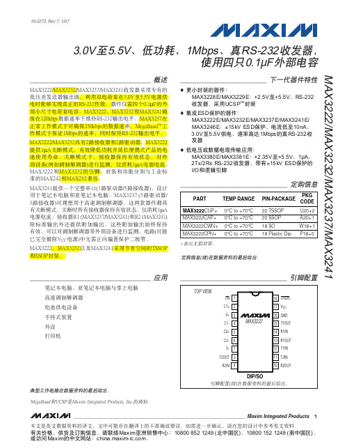
MAX3222/MAX3232/MAX3237/MAX32413.0V至5.5V、低功耗、1Mbps、真RS-232收发器,使用四只0.1µF外部电容________________________________________________________________Maxim Integrated Products119-0273; Rev 7; 1/07MegaBaud和UCSP是Maxim Integrated Products, Inc.的商标。
本文是英文数据资料的译文,文中可能存在翻译上的不准确或错误。
如需进一步确认,请在您的设计中参考英文资料。
有关价格、供货及订购信息,请联络Maxim亚洲销售中心:10800 852 1249 (北中国区),10800 152 1249 (南中国区),或访问Maxim的中文网站:。
M A X 3222/M A X 3232/M A X 3237/M A X 32413.0V至5.5V、低功耗、1Mbps、真RS-232收发器,使用四只0.1µF外部电容2_______________________________________________________________________________________ABSOLUTE MAXIMUM RATINGSELECTRICAL CHARACTERISTICS(V CC = +3.0V to +5.5V, C1–C4 = 0.1µF (Note 2), T A = T MIN to T MAX , unless otherwise noted. Typical values are at T A = +25°C.)Stresses beyond those listed under “Absolute Maximum Ratings” may cause permanent damage to the device. These are stress ratings only, and functional operation of the device at these or any other conditions beyond those indicated in the operational sections of the specifications is not implied. Exposure to absolute maximum rating conditions for extended periods may affect device reliability.Note 1:V+ and V- can have a maximum magnitude of 7V, but their absolute difference cannot exceed 13V.V CC ...........................................................................-0.3V to +6V V+ (Note 1)...............................................................-0.3V to +7V V- (Note 1)................................................................+0.3V to -7V V+ + V- (Note 1)...................................................................+13V Input VoltagesT_IN, SHDN , EN ...................................................-0.3V to +6V MBAUD...................................................-0.3V to (V CC + 0.3V)R_IN.................................................................................±25V Output VoltagesT_OUT...........................................................................±13.2V R_OUT....................................................-0.3V to (V CC + 0.3V)Short-Circuit DurationT_OUT....................................................................ContinuousContinuous Power Dissipation (T A = +70°C)16-Pin TSSOP (derate 6.7mW/°C above +70°C).............533mW 16-Pin Narrow SO (derate 8.70mW/°C above +70°C)....696mW 16-Pin Wide SO (derate 9.52mW/°C above +70°C)........762mW 16-Pin Plastic DIP (derate 10.53mW/°C above +70°C)...842mW 18-Pin SO (derate 9.52mW/°C above +70°C)..............762mW 18-Pin Plastic DIP (derate 11.11mW/°C above +70°C)..889mW 20-Pin SSOP (derate 7.00mW/°C above +70°C).........559mW 20-Pin TSSOP (derate 8.0mW/°C above +70°C).............640mW 28-Pin TSSOP (derate 8.7mW/°C above +70°C).............696mW 28-Pin SSOP (derate 9.52mW/°C above +70°C).........762mW 28-Pin SO (derate 12.50mW/°C above +70°C).....................1W Operating Temperature RangesMAX32_ _C_ _.....................................................0°C to +70°C MAX32_ _E_ _ .................................................-40°C to +85°C Storage Temperature Range.............................-65°C to +150°C Lead Temperature (soldering, 10s).................................+300°CMAX3222/MAX3232/MAX3237/MAX32413.0V至5.5V、低功耗、1Mbps、真RS-232收发器,使用四只0.1µF外部电容_______________________________________________________________________________________3TIMING CHARACTERISTICS—MAX3222/MAX3232/MAX3241(V CC = +3.0V to +5.5V, C1–C4 = 0.1µF (Note 2), T A = T MIN to T MAX , unless otherwise noted. Typical values are at T A = +25°C.)ELECTRICAL CHARACTERISTICS (continued)(V CC = +3.0V to +5.5V, C1–C4 = 0.1µF (Note 2), T A = T MIN to T MAX , unless otherwise noted. Typical values are at T A = +25°C.)A X 3222/M A X 3232/M A X 3237/M A X 32413.0V至5.5V、低功耗、1Mbps、真RS-232收发器,使用四只0.1µF外部电容4_______________________________________________________________________________________典型工作特性Ω, T A = +25°C, unless otherwise noted.)LOAD CAPACITANCE (pF)0246810121416182022150MAX3222/MAX3232SLEW RATEvs. LOAD CAPACITANCELOAD CAPACITANCE (pF)S L E W R A T E (V /µs )20003000100040005000510152025303540MAX3222/MAX3232SUPPLY CURRENT vs. LOAD CAPACITANCEWHEN TRANSMITTING DATALOAD CAPACITANCE (pF)S U P P L Y C U R R E N T (m A )20003000100040005000TIMING CHARACTERISTICS—MAX3237(V CC = +3.0V to +5.5V, C1–C4 = 0.1µF (Note 2), T A = T MIN to T MAX , unless otherwise noted. Typical values are at T A = +25°C.)Note 2:MAX3222/MAX3232/MAX3241: C1–C4 = 0.1µF tested at 3.3V ±10%; C1 = 0.047µF, C2–C4 = 0.33µF tested at 5.0V ±10%.MAX3237: C1–C4 = 0.1µF tested at 3.3V ±5%; C1–C4 = 0.22µF tested at 3.3V ±10%; C1 = 0.047µF, C2–C4 = 0.33µF tested at 5.0V ±10%.Note 3:Transmitter input hysteresis is typically 250mV.MAX3222/MAX3232/MAX3237/MAX32413.0V至5.5V、低功耗、1Mbps、真RS-232收发器,使用四只0.1µF外部电容_______________________________________________________________________________________5-7.5-5.0-2.502.55.07.50MAX3241TRANSMITTER OUTPUT VOLTAGEvs. LOAD CAPACITANCELOAD CAPACITANCE (pF)T R A N S M I T T E R O U T P U T V O L T A G E (V )2000300010004000500046810121416182022240MAX3241SLEW RATEvs. LOAD CAPACITANCELOAD CAPACITANCE (pF)S L E W R A T E (V /µs )20003000100040005000510152025303545400MAX3241SUPPLY CURRENT vs. LOADCAPACITANCE WHEN TRANSMITTING DATALOAD CAPACITANCE (pF)S U P P L Y C U R R E N T (m A )20003000100040005000-7.5-5.0-2.502.55.07.50MAX3237TRANSMITTER OUTPUT VOLTAGE vs. LOAD CAPACITANCE (MBAUD = GND)LOAD CAPACITANCE (pF)T R A N S M I T T E R O U T P U T V O L T A G E (V )200030001000400050000102030504060700MAX3237SLEW RATE vs. LOAD CAPACITANCE(MBAUD = V CC )LOAD CAPACITANCE (pF)S L E W R A T E (V /µs )500100015002000-7.5-5.0-2.502.55.07.50MAX3237TRANSMITTER OUTPUT VOLTAGE vs. LOAD CAPACITANCE (MBAUD = V CC )LOAD CAPACITANCE (pF)T R A N S M I T T E R O U T P U T V O L T A G E (V )5001000150020001020304050600MAX3237SUPPLY CURRENT vs.LOAD CAPACITANCE (MBAUD = GND)LOAD CAPACITANCE (pF)S U P P L Y C U R R E N T (m A )200030001000400050000246810120MAX3237SLEW RATE vs. LOAD CAPACITANCE(MBAUD = GND)LOAD CAPACITANCE (pF)S L E W R A T E (V /µs )2000300010004000500010302040506070MAX3237SKEW vs. LOAD CAPACITANCE(t PLH - t PHL )LOAD CAPACITANCE (pF)1000150050020002500____________________________________________________________________典型工作特性(续)(V CC = +3.3V, 235kbps data rate, 0.1µF capacitors, all transmitters loaded with 3k Ω, T A = +25°C, unless otherwise noted.)M A X 3222/M A X 3232/M A X 3237/M A X 32413.0V至5.5V、低功耗、1Mbps、真RS-232收发器,使用四只0.1µF外部电容6_________________________________________________________________________________________________________________________________________________________________引脚说明MAX3222/MAX3232/MAX3237/MAX32413.0V至5.5V、低功耗、1Mbps、真RS-232收发器,使用四只0.1µF外部电容_______________________________________________________________________________________7_______________________________详细说明双电荷泵电压转换器MAX3222/MAX3232/MAX3237/MAX3241的内部电源由两路稳压型电荷泵组成,只要输入电压(V CC )在3.0V至5.5V范围以内,即可提供+5.5V (倍压电荷泵)和-5.5V (反相电荷泵)输出电压。
国产max3232

国产MAX3232简介MAX3232是一款常用的RS232转换芯片,用于在电脑和外部设备之间传递串行数据。
国产MAX3232是国内厂商生产的一种与MAXIM公司生产的MAX3232功能相似的芯片。
国产MAX3232在功能和参数上与MAX3232基本保持一致,但在价格和供货上具有一定优势。
功能特点1.支持RS232标准,实现电平转换。
2.具有高速数据传输能力,通信稳定可靠。
3.低功耗设计,节能环保。
4.集成了保护功能,具有较好的抗干扰能力。
5.独特的设计使其适用于各种工业和通讯场景。
国产MAX3232与进口MAX3232的比较1.价格:国产MAX3232的价格通常比进口MAX3232更为具有竞争力,降低成本。
2.供货周期:国产MAX3232生产商在国内,供货更为便捷,缩短采购周期。
3.技术支持:国产MAX3232的厂商提供本地化的技术支持,解决问题更为便捷。
4.适用性:国产MAX3232根据国内市场的需求进行定制和优化,更适合国内用户需求。
应用场景1.工控设备:国产MAX3232可广泛应用于工控设备中,实现设备之间的稳定通信。
2.通信设备:在通信设备中,国产MAX3232可以帮助设备与中控系统之间实现数据传输。
3.个人DIY项目:爱好者可以利用国产MAX3232进行串口通信的DIY项目,提高通信稳定性。
结论国产MAX3232是一款功能齐全、价格优势明显的RS232转换芯片,可以满足各类通信设备的需求。
国产MAX3232在本地化支持、技术服务等方面具备诸多优势,为用户提供了更好的使用体验。
在未来的发展中,国产MAX3232有望在国内市场越发广泛地应用于各类通信、工控等领域。
MAX3232每次只有在上电后,再连接串口线正常——保护电阻。RS232防雷保护
MAX3232每次只有在上电后,再连接串⼝线正常——保护电阻。
RS232防雷保护原问题:做了块电路板,结果发现,要先对开发板上电, 再打开串⼝超级终端, 串⼝通信才可成功。
但是另外⼀块开发板却没有这个问题。
这⼀般是什么原因造成的?⾃⼰遇到问题:刚焊接好的板⼦,发现串⼝有问题,结果串⼝每次只有在断电上电后需要在上电后重新连接串⼝线才能正常通信原因简述:缺少保护电阻,解决办法:每次断电时拔掉串⼝线下⾯所提到的问题,和上⾯链接中的问题(热插拔才可通信),其实是同⼀个问题,可能的原因是1. 232收发器芯⽚产⽣电压的那些⼩电容的数值是和数据⼿册上不太⼀致2. 232收发器芯⽚和232插座之间缺少串联保护电阻,或保护电阻数值太⼩。
3. 原来的232收发器芯⽚可能部分失效了如果1和2都已经做到了,将232收发器芯⽚的RXD输⼊管脚和插座RXD之间的串联保护电阻加⼤,⽐如换成1K或10K的,应该就可以了。
如果还不成,就换个232芯⽚吧。
多说⼏句原因吧(以前碰到过该问题所以就研究过):在不通信的时候,PC串⼝的TXD管脚会输出-5V左右的电压,于是在开发板上的232收发器芯⽚的RXD对应的输⼊管脚(R1IN或R2IN)上维持着-5V左右的电压。
当开发板断电时,232收发器芯⽚的电源管脚没有电压,V+/V-管脚也没有电压,唯独RXD输⼊管脚(R1IN或R2IN)上维持这⼀个-5V左右的电平,不⽤多说就能明⽩这意味着什么。
假如习惯上每次给开发板断电后却让串⼝依旧和 PC保持连接,这意味这232收发器芯⽚长期承受着RXD输⼊管脚-5V但同时⼜让电源管脚和V+/V-为零电平,特别当PC的TXD输出维持这超过-5V甚⾄超过-6V的时候,久⽽久之,这颗芯⽚就会渐渐部分失效或全部失效,于是通信就失败了。
所以换⼀个芯⽚往往就可以解决这个问题。
每次先打开串⼝程序⽽没有通信的时候,-5V或以下的电压就加在TXD管脚上了,如果此时开发板断电但是却接着串⼝,就相当于初始状态是先让232收发器芯⽚处于上述异常的⼯作条件,然后再给开发板上电的时候,就可能出现通信不成功的状况。
MAX3232ESE RS232接口芯片应用方案-奥伟斯
奥伟斯科技为您提供RS232接口芯片MAX3232ESE应用参考设计方案●内容导航:●公司简介●MAX3232产品规格书MAX3232ESE MAX3232CSE MAX3232EUE MAX3232EEAE MAX3232EEUE●产品图片●主营产品及优势产品简介●公司简介深圳市奥伟斯科技有限公司是一家专注触摸芯片,单片机,电源管理芯片,语音芯片,场效应管,显示驱动芯片,网络接收芯片,运算放大器,红外线接收头及其它半导体产品的研发,代理销售推广的高新技术企业.奥伟斯科技自成立以来一直致力于新半导体产品在国内的推广与销售,年销售额超过壹亿人民币是一家具有综合竞争优势的专业电子元器件代理商.本公司代理推广的一系列优秀触摸芯片及语音芯片,现以大批量应用到智能电子锁、饮水机、电饭煲、LED台灯等控制器为顾客提供最佳解决方案,受到广大客户的一致赞誉。
奥伟斯科技优势行业集中在家用电器和汽车电子领域,包括:智能电子锁、饮水机、抽烟机、空调、洗衣机、冰箱、洗碗机、电饭煲、电磁炉、微波炉、电动自行车、汽车仪表、汽车音响、汽车空调等。
销售网络覆盖华东、华南及华北地区。
奥伟斯科技已为众多世界著名企业提供服务如:美的、小米、云米、长虹、创维、三星、LG、飞利浦、TCL、海尔、美菱、沁园、等众多中国一流品牌电家厂商奥伟斯科技提供专业的智能电子锁触摸解决方案,并提供电子锁整套的芯片配套:低功耗触摸芯片低功耗单片机马达驱动芯片显示驱动芯片刷卡芯片时针芯片存储芯片语音芯片低压MOS管 TVS二极管主要品牌产品:OWEIS-TECHOWEIS触摸芯片 OWEIS接口芯片 OWEIS电源芯片 OWEIS语音芯片 OWEIS场效应管一.电容式触摸芯片ADSEMI触摸芯片代理芯邦科技触控芯片万代科技触摸按键芯片博晶微触摸控制芯片海栎创触摸感应芯片启攀微触摸IC 融和微触摸感应IC 合泰触摸按键IC 通泰触摸芯片二.汽车电子/电源管理/接口芯片/逻辑芯片:IKSEMICON一级代理 ILN2003ADT IK62783DT IL2596 IL2576 ILX485 ILX3485 ILX232ILX3232三.功率器件/接收头/光电开关:KODENSHI AUK SMK系列MOS管SMK0260F SMK0460F SMK0760F SMK1260F SMK1820F SMK18T50F四. LED显示驱动芯片:中微爱芯AIP系列 AIP1668 AIP1628 AIP1629 AIP1616天微电子TM系列 TM1628 TM1668 TM1621五.电源管理芯片:Power Integrations LNK364PN LNK564PN 芯朋微PN8012 PN8015 AP5054 AP5056 力生美晶源微友达天钰电子FR9886 FR9888六.语音芯片:APLUS巨华电子AP23085 AP23170 AP23341 AP23682 AP89085 AP89170 AP89341AP89341K AP89682七.运算放大器:3PEAK运算放大器聚洵运算放大器圣邦微运算放大器八.发光二极管:OSRAM欧司朗发光二极管 Lite-On光宝发光二极管 Everlight亿光发光二极管 Kingbright今台发光二极管九. CAN收发器:NXP恩智浦CAN收发器 Microchip微芯CAN收发器十.分销产品线:ONSEMI安森美 TI德州仪器 ADI TOSHIBA东芝 AVAGO安华高十一 MCU单片机ABOV现代单片机MC96F系列 Microchip微芯单片机PIC12F PIC16F PIC18F系列 FUJITSU富仕通单片机MB95F系列 STM单片机STM32F STM32L系列 CKS中科芯单片机CKS32F系列 TI单片机MSP430系列 TMS320F系列 NXP单片机LPC系列D, DB, DW, OR PW PACKAGE (TOP VIEW)C1+V+C1−C2+C2−V−DOUT2RIN2Package drawings, standard packing quantities, thermal data, symbolization, and PCB design guidelines areavailable at /sc/package.Please be aware that an important notice concerning availability, standard warranty, and use in critical applications ofTexas Instruments semiconductor products and disclaimers thereto appears at the end of this data s heet.Copyright ©2004, Texas Instruments Incorporated PRODUCTION DATA information is current as of publication date.Products conform to s pecifications p er t he t erms o f Texas Instrumentsstandard warranty. Production processing does not necessarily includetesting of all p arameters.1description/ordering information (continued)The MAX3232 device consists of two line drivers, two line receivers, and a dual charge-pump circuit with ±15-kV ESD protection pin to pin (serial-port connection pins, including GND). The device meets the requirements of TIA/EIA-232-F and provides the electrical interface between an asynchronous communication controller and the serial-port connector. The charge pump and four small external capacitors allow operation from a single 3-V to 5.5-V supply. The devices operate at data signaling rates up to 250 kbit/s and a maximum of 30-V/μs driver output slew rate.Function TablesEACH DRIVERlevelEACH RECEIVERlevel, Open = inputdisconnected orconnected driver offlogic diagram (positive logic)DIN1 DOUT1DIN2 DOUT2ROUT1 RIN1ROUT2 RIN22absolute maximum ratings over operating free-air temperature range (unless otherwise noted)†Supply voltage range, V CC (see Note 1) . . . . . . . . . . . . . . . . . . . . . . . . . . . . . . . . . . . . . . . . . . . . . .−0.3 V to 6 VPositive output supply voltage range, V+ (see Note 1) Negative output supply voltage range, V− (see Note 1). . . . . . . . . . . . . . . . . . . . . . . . . . . . . . . . . .. . . . . . . . . . . . . . . . . . . . . . . . . . . . . . . . .−0.3 V to 7 V0.3 V to −7 VSupply voltage difference, V+ −V− (see Note 1). . . . . . . . . . . . . . . . . . . . . . . . . . . . . . . . . . . . . . . . . . . . . .13 V Input voltage range, V I: Drivers . . . . . . . . . . . . . . . . . . . . . . . . . . . . . . . . . . . . . . . . . . . . . . . . . . . . . .−0.3 V to 6 V Receivers ............................................................................................... −25 V to 25 V Output voltage range, V O: Drivers.......................................................................................... −13.2 V to 13.2 VReceivers .............................................................................. −0.3 V to V CC + 0.3 VPackage thermal impedance, θJA (see Notes 2 and 3): D packageDB package . . . . . . . . . . . . . . . . . . . . . . . . . . . .. . . . . . . . . . . . . . . . . . . . . . . . . . .73︒C/W82︒C/WDW package. . . . . . . . . . . . . . . . . . . . . . . . . . 57︒C/WPW package .................................................108︒C/W Operating virtual junction temperature, T J . . . . . . . . . . . . . . . . . . . . . . . . . . . . . . . . . . . . . . . . . . . . . . . . . . .150︒C Storage temperature range, T stg . . . . . . . . . . . . . . . . . . . . . . . . . . . . . . . . . . . . . . . . . . . . . . . . . . .−65︒C to 150︒C† Stresses beyond those listed under “absolute maximum ratings” may cause permanent damage to the device. These are stress ratings only, and functional operation of the device at these or any other conditions beyond those indicated under “recommended operating conditions” is not implied. Exposure to absolute-maximum-rated conditions for extended periods may affect device reliability.NOTES: 1. All voltages are with respect to network GND.2. Maximum power dissipation is a function of T J(max), θJA, and T A. The maximum allowable power dissipation at any allowableambient temperature is P D = (T J(max) − T A)/θJA. Operating at the absolute maximum T J of 150︒C can affect reliability.3. The package thermal impedance is calculated in accordance with JESD 51-7.recommended operating conditions (see Note 4 and Figure 4)CC CCelectrical characteristics over recommended ranges of supply voltage and operating free-air temperature (unless otherwise noted) (see Note 4 and Figure 4)All typical values are at V CC = 3.3 V or V CC = 5 V, and T A = 25︒C.NOTE 4: Test conditions are C1−C4 = 0.1 μF at V CC = 3.3 V ±0.3 V; C1 = 0.047 μF, C2−C4 = 0.33 μF at V CC = 5 V ±0.5 V.3DRIVER SECTIONelectrical characteristics over recommended ranges of supply voltage and operating free-air temperature (unless otherwise noted) (see Note 4 and Figure 4)CC CC A‡ Short-circuit durations should be controlled to prevent exceeding the device absolute power dissipation ratings, and not more than one output should be shorted at a time.NOTE 4: Test conditions are C1−C4 = 0.1 μF at V CC = 3.3 V ±0.3 V; C1 = 0.047 μF, C2−C4 = 0.33 μF at V CC = 5 V ±0.5 V.switching characteristics over recommended ranges of supply voltage and operating free-air temperature (unless otherwise noted) (see Note 4 and Figure 4)CC CC A§Pulse skew is defined as |t PLH − t PHL| of each channel of the same device.NOTE 4: Test conditions are C1−C4 = 0.1 μF at V CC = 3.3 V ±0.3 V; C1 = 0.047 μF, C2−C4 = 0.33 μF at V CC = 5 V ±0.5 V.4RECEIVER SECTIONelectrical characteristics over recommended ranges of supply voltage and operating free-air temperature (unless otherwise noted) (see Note 4 and Figure 4)CC CC A NOTE 4: Test conditions are C1−C4 = 0.1 μF at V CC = 3.3 V ± 0.3 V; C1 = 0.047 μF, C2−C4 = 0.33 μF at V CC = 5 V ± 0.5 V.switching characteristics over recommended ranges of supply voltage and operating free-air temperature (unless otherwise noted) (see Note 4 and Figure 3)CC CC A ‡ Pulse skew is defined as |t PLH − t PHL | of each channel of the same device.NOTE 4: Test conditions are C1−C4 = 0.1 μF at V CC = 3.3 V ± 0.3 V; C1 = 0.047 μF, C2−C4 = 0.33 μF at V CC = 5 V ± 0.5 V.PARAMETER MEASUREMENT INFORMATIONGenerator (see Note B)50 ΩRS-232 OutputC LInputt THL3 V 0 V t TLHR L(see Note A)Output3 V−3 V 3 V−3 VV OHV OLTEST CIRCUITSR(tr) = 6 V t THL or t TLHVOLTAGE WAVEFORMSNOTES: A. C L includes probe and jig capacitance.B. The pulse generator has the following characteristics: PRR = 250 kbit/s, Z O = 50 Ω, 50% duty cycle, t r ≤ 10 ns, t f ≤ 10 ns.Figure 1. Driver Slew Rate5PARAMETER MEASUREMENT INFORMATIONGenerator(see Note B)50 ΩRS-232OutputC L3 VInput0 V R LTEST CIRCUIT NOTES: A. C L includes probe and jig capacitance.(see Note A)OutputVOLTAGE WAVEFORMSV OHV OLB. The pulse generator has the following characteristics: PRR = 250 kbit/s, Z O = 50 Ω, 50% duty cycle, t r ≤10 ns, t f ≤10 ns.Figure 2. Driver Pulse SkewGenerator(see Note B)50 ΩOutputC LInput3 V−3 VTEST CIRCUIT (see Note A)OutputVOLTAGE WAVEFORMSV OHV OLNOTES: A. C L includes probe and jig capacitance.B. The pulse generator has the following characteristics: Z O = 50 Ω, 50% duty cycle, t r ≤10 ns, t f ≤10 ns.Figure 3. Receiver Propagation Delay Times6−APPLICATION INFORMATION+C1 †+C31C1+2 V+V CC 16GND15+ C BYPASS−= 0.1μF−+C2−−C4+ DOUT23C1−4C2+5 C2−6V−714135 kΩ121110DOUT1RIN1ROUT1DIN1DIN2RIN2 8 9ROUT25 kΩ† C3 can be connected to V CC or GND.NOTES: A. Resistor values shown are nominal.B. Nonpolarized ceramic capacitors are acceptable. If polarized tantalum or electrolytic capacitors are used, they should beconnected as shown.Vvs CAPACITOR VALUESFigure 4. Typical Operating Circuit and Capacitor Values7PACKAGE OPTION ADDENDUM 14-Aug-2009 PACKAGING INFORMATIONAddendum-Page 1PACKAGE OPTION ADDENDUM(1) The marketing status values are defined as follows:ACTIVE: Product device recommended for new designs.LIFEBUY: TI has announced that the device will be discontinued, and a lifetime-buy period is in effect.NRND: Not recommended for new designs. Device is in production to support existing customers, but TI does not recommend using this part in a new design.PREVIEW: Device has been announced but is not in production. Samples may or may not be available.OBSOLETE: TI has discontinued the production of the device.(2) Eco Plan - The planned eco-friendly classification: Pb-Free (RoHS), Pb-Free (RoHS Exempt), or Green (RoHS & no Sb/Br) - please check /productcontent for the latest availability information and additional product content details.PACKAGE OPTION ADDENDUM14-Aug-2009 TBD: The Pb-Free/Green conversion plan has not been defined.Pb-Free (RoHS): TI's terms "Lead-Free" or "Pb-Free" mean semiconductor products that are compatible with the current RoHS requirements for all 6 substances, including the requirement that lead not exceed 0.1% by weight in homogeneous materials. Where designed to be soldered at high temperatures, TI Pb-Free products are suitable for use in specified lead-free processes.Pb-Free (RoHS Exempt): This component has a RoHS exemption for either 1) lead-based flip-chip solder bumps used between the die and package, or 2) lead-based die adhesive used between the die and leadframe. The component is otherwise considered Pb-Free (RoHS compatible) as defined above.Green (RoHS & no Sb/Br): TI defines "Green" to mean Pb-Free (RoHS compatible), and free of Bromine (Br) and Antimony (Sb) based flame retardants (Br or Sb do not exceed 0.1% by weight in homogeneous material)(3) MSL, Peak Temp. -- The Moisture Sensitivity Level rating according to the JEDEC industry standard classifications, and peak solder temperature.Important Information and Disclaimer:The information provided on this page represents TI's knowledge and belief as of the date that it is provided. TI bases its knowledge and belief on information provided by third parties, and makes no representation or warranty as to the accuracy of such information. Efforts are underway to better integrate information from third parties. TI has taken and continues to take reasonable steps to provide representative and accurate information but may not have conducted destructive testing or chemical analysis on incoming materials and chemicals. TI and TI suppliers consider certain information to be proprietary, and thus CAS numbers and other limited information may not be available for release.In no event shall TI's liability arising out of such information exceed the total purchase price of the TI part(s) at issue in this document sold by TI to Customer on an annual basis.OTHER QUALIFIED VERSIONS OF MAX3232 :•Enhanced Product: MAX3232-EPNOTE: Qualified Version Definitions:•Enhanced Product - Supports Defense, Aerospace and Medical ApplicationsTAPE AND REEL INFORMATIONDB (R-PDSO-G**) PLASTIC SMALL-OUTLINE 28 PINS SHOWNNOTES: A. All linear dimensions are in millimeters.B. This drawing is subject to change without notice.C. Body dimensions do not include mold flash or protrusion not to exceed 0,15.D. Falls within JEDEC MO-150PW (R-PDSO-G**) PLASTIC SMALL-OUTLINE PACKAGE 14 PINS SHOWNNOTES: A. All linear dimensions are in millimeters.B. This drawing is subject to change without notice.C. Body dimensions do not include mold flash or protrusion not to exceed 0,15.D. Falls within JEDEC MO-153IMPORTANT NOTICETexas Instruments Incorporated and its subsidiaries (TI) reserve the right to make corrections, modifications, enhancements, improvements, and other changes to its products and services at any time and to discontinue any product or service without notice. Customers should obtain the latest relevant information before placing orders and should verify that such information is current and complete. All products are sold subject to TI’s terms and conditions of sale supplied at the time of order acknowledgment.TI warrants performance of its hardware products to the specifications applicable at the time of sale in accordance with TI’s standard warranty. Testing and other quality control techniques are used to the extent TI deems necessary to support this warranty. Except where mandated by government requirements, testing of all parameters of each product is not necessarily performed.TI assumes no liability for applications assistance or customer product design. Customers are responsible for their products and applications using TI components. To minimize the risks associated with customer products and applications, customers should provide adequate design and operating safeguards.TI does not warrant or represent that any license, either express or implied, is granted under any TI patent right, copyright, mask work right, or other TI intellectual property right relating to any combination, machine, or process in which TI products or services are used. Information published by TI regarding third-party products or services does not constitute a license from TI to use such products or services or a warranty or endorsement thereof. Use of such information may require a license from a third party under the patents or other intellectual property of the third party, or a license from TI under the patents or other intellectual property of TI.Reproduction of TI information in TI data books or data sheets is permissible only if reproduction is without alteration and is accompanied by all associated warranties, conditions, limitations, and notices. Reproduction of this information with alteration is an unfair and deceptive business practice. TI is not responsible or liable for such altered documentation. Information of third parties may be subject to additional restrictions.Resale of TI products or services with statements different from or beyond the parameters stated by TI for that product or service voids all express and any implied warranties for the associated TI product or service and is an unfair and deceptive business practice. TI is not responsible or liable for any such statements.TI products are not authorized for use in safety-critical applications (such as life support) where a failure of the TI product would reasonably be expected to cause severe personal injury or death, unless officers of the parties have executed an agreement specifically governing such use. Buyers represent that they have all necessary expertise in the safety and regulatory ramifications of their applications, and acknowledge and agree that they are solely responsible for all legal, regulatory and safety-related requirements concerning their products and any use of TI products in such safety-critical applications, notwithstanding any applications-related information or support that may be provided by TI. Further, Buyers must fully indemnify TI and its representatives against any damages arising out of the use of TI products in such safety-critical applications.TI products are neither designed nor intended for use in military/aerospace applications or environments unless the TI products are specifically designated by TI as military-grade or "enhanced plastic." Only products designated by TI as military-grade meet military specifications. Buyers acknowledge and agree that any such use of TI products which TI has not designated as military-grade is solely at the Buyer's risk, and that they are solely responsible for compliance with all legal and regulatory requirements in connection with such use. TI products are neither designed nor intended for use in automotive applications or environments unless the specific TI products are designated by TI as compliant with ISO/TS 16949 requirements. Buyers acknowledge and agree that, if they use any non-designated products in automotive applications, TI will not be responsible for any failure to meet such requirements.Following are URLs where you can obtain information on other Texas Instruments products and application solutions:奥伟斯科技提供专业的智能电子锁触摸解决方案,并提供电子锁整套的芯片配套:低功耗触摸芯片低功耗单片机马达驱动芯片显示驱动芯片刷卡芯片时针芯片存储芯片语音芯片低压MOS管 TVS二极管低功耗触摸按键芯片OWEIS奥伟斯触摸芯片:JM01S JM02S JM04S JM08S JM12MCOWEIS奥伟斯电源芯片: JM2575S-12 JM2575S-3.3 JM2575S-5.0 JM2575S-ADJ JM2575T-12 JM2575T-3.3 JM2575T-5.0 JM2575T-ADJ JM2576S-12 JM2576S-3.3 JM2576S-5.0 JM2576S-ADJ JM2576T-12 JM2576T-3.3 JM2576T-5.0 JM2576T-ADJ LM2596S-12 LM2596S-3.3 LM2596S-5.0 LM2596S-ADJ LM2596T-12 LM2596T-3.3 LM2596T-5.0 LM2596T-ADJ OWEIS奥伟斯接口芯片:JM485S JM3485S JM232S JM232TS JM3232S JM3232TS JM1040SOWEIS语音芯片:JM085S JM170S JM341S JM682SADS触摸芯片:TQ01 TS01Q TQ02 TH01TS01S AWS01 TS02NT TS04 TS06 TS08NT TS08NC TS08NE TS08P TS12 TSM12S TSM12MC TSM16C TS20博晶微/晶尊微触摸芯片:SC01A SC02A SC04A SC05A SC09A SC12A通泰触控芯片: TTP223-BA6 TTP223-CA6 TTP223N-BA6 TTP223N-HA6 TTP223N-CA6 TTP223N-DO8 TTP233B-BA6TTP233B-HA6 TTP233C-BA6 TTP233C-HA6 TTP233D-HA6 TTP233D-BA6 TTP233D-QA6 TTP233D-MA6 TTP233D-RB6TTP233D-SB6 TTP239-BSF TTP239-COBN TTP223E TTP223E-BA6 TTP223E-CA6 TTP223E-HA6 TTP233F-QA6 TTP226-809SN TTP259-ASFN TTP229-AQG TTP229-BSF TTP229-LSFN TTP229-KSFN TTP232-BA6 TTP232-CA6 TTP224B TTP224B-BSBN TTP224B-BSBN TTP224B-COBN TTP224B-COBN TTP224B-SQBN TTP224B-RO8N TTP224B-BCBN TTP224B-RC8N TTY6952B合泰触摸控制芯片:BS801B BS801C BS802B BS802C BS804B BS804C BS806B BS806C BS808B BS808C BS83A04A-3BS83B08-3 BS83B08A-3 BS83B08A-4 BS83A02A-4 BS83A02A-4 BS83A02A-4 BS83A04A-3 BS83A04A-4 BS83B08A-3BS83B08A-4 BS83B12A-3 BS83B12A-3 BS83B12A-4 BS83B12A-4 BS83B16A-3 BS83B16A-3 BS83B16A-4 BS83B16A-4BS82B12A-3 BS82C16A-3 BS82D20A-3 BS83A01C BS83A02C BS83B04C BS83B08C BS83B12C BS83B16C BS83B24CBS83C40C BS83B08-3 BS83B12-3 BS83B16-3 BS83C24-3 BS83C24-3 BS84B08A-3 BS84B08A-3 BS84B08A-3 BS84B08A-3 BS84B08A-3 BS84B08A-3 BS84C12A-3 BS84C12A-3 BS84C12A-3 BS84C12A-3 BS84C12A-3 BS84C12A-3低功耗单片机:STM8L052C6T6 STM8L052R8T6 STM8L152C6T6 STM8L152R8T6 STM32L151C8T6 STM32L152RBT6STM32L051C8T6指纹识别芯片:AS608 QS808马达驱动芯片:MX08E L9110S BA6287F-E2显示驱动芯片:74HC595PW 74HC164PW刷卡芯片:MFRC52202HN1/RC522 MFCV520/CV520 FM17520 FM17522 MS520 MS522时针芯片:PCF8563T AIP8536 IN1363DT VC8563T DQ8563T存储芯片:W25Q32JVSSIQ W25Q32BVSSIG W25Q32FVSSIG AT24C32D-SSHM-T GD25Q32BSIG GD25Q32CSIG FM25Q32 FM24C32 语音芯:AP23085 AP23341 AP89085 AP89341K低压MOS管:SI2300 SI2301 SI2302 AO3400 AO3401 AO3402TVS二极管:SMAJ6.0CA SMAJ15CACAN收发器:TJA1040T TJA1042T TJA1043T TJA1044T TJA1050T TJA1051T TJA1052T TJA1053T MCP2515-I/SO MCP2515T-I/SO MCP2515-I/ST MCP2515T-I/ST网络接口芯片:MAX485ESA MAX485EESA MAX485CSA MAX485ED ST3485EBDR ST3485ECDR ADM485ARZ ADM485EARZ SP485EN SP485EEN ILX485DT MAX4853ESA MAX3485EESA MAX3485CSA ST3485EBDR ST3485ECDR ADM3485ARZ ADM3485EARZ SP3485EN SP3485EEN ILX3485DT MAX232ESE MAX232EESE MAX232CSE MAX232DR MAX232IDRMAX232EIDR ST232BDR ST232CDR ST232EBDR ST232ABDR ADM232AARNZ ADM232AARW ADM232LAR SP232ECNSP232EEN ILX232DT MAX232EIPWR ST232BTR ST232ABTR ST232CTR ST232ACTR MAX3232ESE MAX3232EESEMAX3232CSE MAX3232CDR MAX3232ECDR MAX3232IDR MAX3232EIDR ST3232CDR ST3232BDR ST3232EBDRST3232ECDR ADM3232EARN SP3232EEN ILX3232DT MAX3232EEAE ST3232CTR ST3232BTR ST3232EBTR ST3232ECTR ADM3232EARUZ SP3232EEA SP3232EEY ILX3232TSDT电源管理芯片:LM2575 LM2576 LM2596 IL2576 IL2596 XL2596 XL2576 TD2576 TD2596ADI模数转换器:AD7705BRZ AD7705BURZ AD7706BRZ AD7706BURZ AD7715ANZ-3 AD7715ANZ-5 AD7715ARZ-3REELAD7715ARZ-5REELAMS奥地利微低频唤醒芯片:AS3933-BTST AS3933-BQFTCKS中科芯单片机:CKS32F030K6T6 CKS32F030C8T6 CKS32F051C8T6 CKS32F051R8T6 CKS32F103C8T6CKS32F103R8T6聚洵运算放大器:聚洵零漂移运算放大器GS8592-SR GS8592-MR GS8594-TR GS8594-SR GS6554-TR GS6554-SR GS6552-SR GS6552-MR GS6551-CR GS6551-TR GS8551-TR GS8551-SR GS8552-SR GS8552-MR GS8554-TR GS8554-SR GS8331-TRGS8331-CR GS8331-SR GS8331Y-TR GS8331Y-CR GS8332-SR GS8332-MR GS8332-FR GS8334-TR GS8334-SR聚洵高速运算放大器:GS8091-CR GS8091-TR GS8091N-CR GS8091N-TR GS8092-SR GS8092-MR GS8092N-MRGS8094-TR GS8094-SR GS8054-TR GS8054-SR GS8052N-MR GS8052-SR GS8052-MR GS8051N-CR GS8051N-TRGS8051-CR GS8051-TR聚洵高精度运算放大器:GS358-SR GS358-MR GS358-DR GS358-FR GS321Y-CR GS321Y-TR GS321-CR GS321-TR GS8721-CR GS8721-TR GS8721-SR GS8722-SR GS8722-MR GS8724-TR GS8724-SR GS8631-CR GS8631-TR GS8631-SR GS8632-SR GS8632-MR GS8634-TR GS8634-SR GS8631N-TR聚洵纳安级运算放大器:GS6041-CR GS6041-TR GS6041-SR GS6041-MR GS6042-SR GS6042-MR GS6042-FRGS6043-SR GS6043-MR GS6044-TR GS6044-SR聚洵高压摆率运放:GS2771-TR GS2772-SR GS2772-MR GS2774-TR GS2774-SR GS2771N-TR聚洵低电压低功耗运算放大器:GS6001A-CR GS6001A-TR GS6001-CR GS6001-TR GS6001Y-CR GS6001Y-TRGS6002-SR GS6002-MR GS6004-SR GS6004-MR优势产品未尽详细,欢迎来电查询!!!。
MAX3232中文资料_数据手册_参数

max3232e

FEATURES APPLICATIONSD, DB, DW, OR PW PACKAGE(TOP VIEW)1 2 3 4 5 6 7 816 15 14 13 12 11 10 9C1+V+C1−C2+C2−V−DOUT2RIN2V CC GND DOUT1 RIN1 ROUT1 DIN1 DIN2 ROUT2DESCRIPTION/ORDERING INFORMATION MAX3232E3-V TO5.5-V MULTICHANNEL RS-232LINE DRIVER/RECEIVERWITH±15-kV IEC ESD PROTECTIONSLLS664A–AUGUST2005–REVISED APRIL2007•Battery-Powered Systems•ESD Protection for RS-232Bus Pins•PDAs–±15kV(HBM)•Notebooks–±8kV(IEC61000-4-2,Contact Discharge)•Laptops–±15kV(IEC61000-4-2,Air-Gap Discharge)•Palmtop PCs•Meets or Exceeds the Requirements of•Hand-Held EquipmentTIA/EIA-232-F and ITU v.28Standards•Operates With3-V to5.5-V V CC Supply•Operates up to250kbit/s•Two Drivers and Two Receivers•Low Supply Current...300µA Typ•External Capacitors...4×0.1µF•Accepts5-V Logic Input With3.3-V Supply•Pin Compatible to Alternative High-SpeedDevice(1Mbit/s)–SNx5C3232ORDERING INFORMATIONT A PACKAGE(1)(2)ORDERABLE PART NUMBER TOP-SIDE MARKINGTube of40MAX3232ECDSOIC–D MAX3232ECReel of2500MAX3232ECDRTube of40MAX3232ECDWSOIC–DW MAX3232ECReel of2000MAX3232ECDWR–0°C to70°CTube of80MAX3232ECDBSSOP–DB MP232ECReel of2000MAX3232ECDBRTube of90MAX3232ECPWTSSOP–PW MP232ECReel of2000MAX3232ECPWRTube of40MAX3232EIDSOIC–D MAX3232EIReel of2500MAX3232EIDRTube of40MAX3232EIDWSOIC–DW MAX3232EIReel of2000MAX3232EIDWR–40°C to85°CTube of80MAX3232EIDBSSOP–DB MP232EIReel of2000MAX3232EIDBRTube of90MAX3232EIPWTSSOP–PW MP232EIReel of2000MAX3232EIPWR(1)Package drawings,standard packing quantities,thermal data,symbolization,and PCB design guidelines are available at/sc/package.(2)For the most current package and ordering information,see the Package Option Addendum at the end of this document,or see the TIwebsite at .Please be aware that an important notice concerning availability,standard warranty,and use in critical applications of TexasInstruments semiconductor products and disclaimers thereto appears at the end of this data sheet.DESCRIPTION/ORDERING INFORMATION (CONTINUED)DIN1DOUT1RIN1ROUT1DIN2DOUT2RIN2ROUT2MAX3232E3-V TO 5.5-V MULTICHANNEL RS-232LINE DRIVER/RECEIVER WITH ±15-kV IEC ESD PROTECTIONSLLS664A–AUGUST 2005–REVISED APRIL 2007The MAX3232E device consists of two line drivers,two line receivers,and a dual charge-pump circuit with ±15-kV IEC ESD protection pin to pin (serial-port connection pins,including GND).The device meets the requirements of TIA/EIA-232-F and provides the electrical interface between an asynchronous communication controller and the serial-port connector.The charge pump and four small external capacitors allow operation from a single 3-V to 5.5-V supply.The devices operate at data signaling rates up to 250kbit/s and a maximum of 30-V/µs driver output slew rate.FUNCTION TABLES EACH DRIVER (1)INPUT OUTPUT DIN DOUTL H HL(1)H =high level,L =low levelEACH RECEIVER (1)INPUT OUTPUT RIN ROUTL H H L OpenH(1)H =high level,L =low level,Open =input disconnected or connected driver offLOGIC DIAGRAM (POSITIVE LOGIC)Absolute Maximum Ratings(1) Recommended Operating Conditions(1) Electrical Characteristics(1)MAX3232E3-V TO5.5-V MULTICHANNEL RS-232LINE DRIVER/RECEIVERWITH±15-kV IEC ESD PROTECTIONSLLS664A–AUGUST2005–REVISED APRIL2007 over operating free-air temperature range(unless otherwise noted)MIN MAX UNITV CC Supply voltage range(2)–0.36VV+Positive output supply voltage range(2)–0.37VV–Negative output supply voltage range(2)0.3–7VV+–Supply voltage difference(2)13VV–Drivers–0.36VV I Input voltage rangeReceivers–2525VDrivers–13.213.2VV O Output voltage rangeReceivers–0.3V CC+0.3VD package73DB package82θJA Package thermal impedance(3)(4)°C/WDW package57PW package108T J Operating virtual junction temperature150°CT stg Storage temperature range–65150°C (1)Stresses beyond those listed under"absolute maximum ratings"may cause permanent damage to the device.These are stress ratingsonly,and functional operation of the device at these or any other conditions beyond those indicated under"recommended operating conditions"is not implied.Exposure to absolute-maximum-rated conditions for extended periods may affect device reliability.(2)All voltages are with respect to network GND.(3)Maximum power dissipation is a function of T J(max),θJA,and T A.The maximum allowable power dissipation at any allowable ambienttemperature is P D=(T J(max)–T A)/θJA.Operating at the absolute maximum T J of150°C can affect reliability.(4)The package thermal impedance is calculated in accordance with JESD51-7.See Figure4MIN NO MAX UNITMV CC=3.3V3 3.3 3.6 Supply voltage VV CC=5V 4.55 5.5V CC=3.3V2 5.5V IH Driver high-level input voltage DIN VV CC=5V 2.4 5.5V IL Driver low-level input voltage DIN00.8VV I Receiver input voltage–2525VMAX3232EC070T A Operating free-air temperature°CMAX3232EI–4085(1)Test conditions are C1–C4=0.1µF at V CC=3.3V±0.3V;C1=0.047µF,C2–C4=0.33µF at V CC=5V±0.5V.over recommended ranges of supply voltage and operating free-air temperature(unless otherwise noted)(see Figure4) PARAMETER TEST CONDITIONS MIN TYP(2)MAX UNITI CC Supply current No load,V CC=3.3V or5V0.31mA(1)Test conditions are C1–C4=0.1µF at V CC=3.3V±0.3V;C1=0.047µF,C2–C4=0.33µF at V CC=5V±0.5V.(2)All typical values are at V CC=3.3V or V CC=5V,and T A=25°C.DRIVER SECTIONElectrical Characteristics (1)Switching Characteristics (1)MAX3232E3-V TO 5.5-V MULTICHANNEL RS-232LINE DRIVER/RECEIVER WITH ±15-kV IEC ESD PROTECTIONSLLS664A–AUGUST 2005–REVISED APRIL 2007over recommended ranges of supply voltage and operating free-air temperature (unless otherwise noted)(see Figure 4)PARAMETERTEST CONDITIONSMIN TYP (2)MAXUNIT V OH High-level output voltage DOUT at R L =3k Ωto GND,DIN =GND 5 5.4V V OL Low-level output voltage DOUT at R L =3k Ωto GND,DIN =V CC–5–5.4V I IH High-level input current V I =V CC ±0.01±1µA I IL Low-level input current V I at GND ±0.01±1µA V CC =3.6V,V O =0V I OS (3)Short-circuit output current ±35±60mA V CC =5.5V,V O =0V r O Output resistanceV CC ,V+,and V–=0V,V O =±2V30010MΩ(1)Test conditions are C1–C4=0.1µF at V CC =3.3V ±0.3V;C1=0.047µF,C2–C4=0.33µF at V CC =5V ±0.5V.(2)All typical values are at V CC =3.3V or V CC =5V,and T A =25°C.(3)Short-circuit durations should be controlled to prevent exceeding the device absolute power dissipation ratings,and not more than one output should be shorted at a time.over recommended ranges of supply voltage and operating free-air temperature (unless otherwise noted)(see Figure 4)PARAMETER TEST CONDITIONSMIN TYP (2)MAXUNIT C L =1000pF,R L =3k Ω,Maximum data rate150250kbit/s One DOUT switching,See Figure 1C L =150pF to 2500pF,R L =3k Ωto 7k Ω,t sk(p)Pulse skew (3)300ns See Figure 2C L =150pF to 1000pF 630Slew rate,transition region R L =3k Ωto 7k Ω,SR(tr)V/µs(see Figure 1)V CC =3.3VC L =150pF to 2500pF430(1)Test conditions are C1–C4=0.1µF at V CC =3.3V ±0.3V;C1=0.047µF,C2–C4=0.33µF at V CC =5V ±0.5V.(2)All typical values are at V CC =3.3V or V CC =5V,and T A =25°C.(3)Pulse skew is defined as |t PLH –t PHL |of each channel of the same device.RECEIVER SECTION Electrical Characteristics(1)Switching Characteristics(1)MAX3232E 3-V TO5.5-V MULTICHANNEL RS-232LINE DRIVER/RECEIVERWITH±15-kV IEC ESD PROTECTIONSLLS664A–AUGUST2005–REVISED APRIL2007over recommended ranges of supply voltage and operating free-air temperature(unless otherwise noted)(see Figure4) PARAMETER TEST CONDITIONS MIN TYP(2)MAX UNITV OH High-level output voltage I OH=–1mA V CC–0.6V CC–0.1V V OL Low-level output voltage I OL=1.6mA0.4VV CC=3.3V 1.5 2.4V IT+Positive-going input threshold voltage VV CC=5V 1.8 2.4V CC=3.3V0.6 1.2V IT–Negative-going input threshold voltage VV CC=5V0.8 1.5V hys Input hysteresis(V IT+–V IT–)0.3V r i Input resistance V I=±3V to±25V357kΩ(1)Test conditions are C1–C4=0.1µF at V CC=3.3V±0.3V;C1=0.047µF,C2–C4=0.33µF at V CC=5V±0.5V.(2)All typical values are at V CC=3.3V or V CC=5V,and T A=25°C.over recommended ranges of supply voltage and operating free-air temperature(unless otherwise noted)(see Figure3)PARAMETER TEST CONDITIONS TYP(2)UNITt PLH Propagation delay time,low-to high-level output300nsC L=150pFt PHL Propagation delay time,high-to low-level output300ns t sk(p)Pulse skew(3)300ns(1)Test conditions are C1–C4=0.1µF at V CC=3.3V±0.3V;C1=0.047µF,C2–C4=0.33µF at V CC=5V±0.5V.(2)All typical values are at V CC=3.3V or V CC=5V,and T A=25°C.(3)Pulse skew is defined as|t PLH–t PHL|of each channel of the same device.PARAMETER MEASUREMENT INFORMATIONTEST CIRCUITVOLTAGE WAVEFORMS0 V3 VOutputInputV OLV OH t TLHRS-232Outputt THLSR(tr)+6V tTHLor tTLHNOTES: A.C L includes probe and jig capacitance.B.The pulse generator has the following characteristics: PRR = 250 kbit/s, Z O = 50 Ω, 50% duty cycle, t r ≤ 10 ns, t f ≤ 10 ns.1.5 V1.5 V3 V −3 V3 V −3 VTEST CIRCUITVOLTAGE WAVEFORMS 0 V 3 VOutputInputV OLV OHt PLHt PHL50%50%NOTES: A.C L includes probe and jig capacitance.B.The pulse generator has the following characteristics: PRR = 250 kbit/s, Z O = 50 Ω, 50% duty cycle, t r ≤ 10 ns, t f ≤ 10 ns.1.5 V1.5 VRS-232OutputTEST CIRCUITVOLTAGE WAVEFORMS50%50%−3 V3 V1.5 V1.5 VOutputInputV OLV OHt PHLt PLHOutputNOTES: A.C L includes probe and jig capacitance.B.The pulse generator has the following characteristics: Z O = 50 Ω, 50% duty cycle, t r ≤ 10 ns, t f ≤ 10 ns.MAX3232E3-V TO 5.5-V MULTICHANNEL RS-232LINE DRIVER/RECEIVER WITH ±15-kV IEC ESD PROTECTIONSLLS664A–AUGUST 2005–REVISED APRIL 2007Figure 1.Driver Slew RateFigure 2.Driver Pulse SkewFigure 3.Receiver Propagation Delay TimesAPPLICATION INFORMATIONC1C BYPASS = 0.1µFV CC C1C2, C3, C43.3 V ± 0.3 V 5 V ± 0.5 V 3 V to 5.5 V0.1 µF 0.047 µF 0.1 µF0.1 µF 0.33 µF 0.47 µFV CC vs CAPACITOR VALUES †C3 can be connected to V CC or GND.NOTES: A.Resistor values shown are nominal.B.Nonpolarized ceramic capacitors are acceptable. If polarized tantalum or electrolytic capacitors are used, they should beconnected as shown.MAX3232E3-V TO 5.5-V MULTICHANNEL RS-232LINE DRIVER/RECEIVERWITH ±15-kV IEC ESD PROTECTIONSLLS664A–AUGUST 2005–REVISED APRIL 2007Figure 4.Typical Operating Circuit and Capacitor ValuesPACKAGING INFORMATIONOrderable Device Status(1)PackageType PackageDrawingPins PackageQtyEco Plan(2)Lead/Ball Finish MSL Peak Temp(3)MAX3232ECD ACTIVE SOIC D1640Green(RoHS&no Sb/Br)CU NIPDAU Level-1-260C-UNLIMMAX3232ECDB ACTIVE SSOP DB1680Green(RoHS&no Sb/Br)CU NIPDAU Level-1-260C-UNLIMMAX3232ECDBE4ACTIVE SSOP DB1680Green(RoHS&no Sb/Br)CU NIPDAU Level-1-260C-UNLIMMAX3232ECDBG4ACTIVE SSOP DB1680Green(RoHS&no Sb/Br)CU NIPDAU Level-1-260C-UNLIMMAX3232ECDBR ACTIVE SSOP DB162000Green(RoHS&no Sb/Br)CU NIPDAU Level-1-260C-UNLIMMAX3232ECDBRE4ACTIVE SSOP DB162000Green(RoHS&no Sb/Br)CU NIPDAU Level-1-260C-UNLIMMAX3232ECDBRG4ACTIVE SSOP DB162000Green(RoHS&no Sb/Br)CU NIPDAU Level-1-260C-UNLIMMAX3232ECDE4ACTIVE SOIC D1640Green(RoHS&no Sb/Br)CU NIPDAU Level-1-260C-UNLIMMAX3232ECDG4ACTIVE SOIC D1640Green(RoHS&no Sb/Br)CU NIPDAU Level-1-260C-UNLIMMAX3232ECDR ACTIVE SOIC D162500Green(RoHS&no Sb/Br)CU NIPDAU Level-1-260C-UNLIMMAX3232ECDRE4ACTIVE SOIC D162500Green(RoHS&no Sb/Br)CU NIPDAU Level-1-260C-UNLIMMAX3232ECDRG4ACTIVE SOIC D162500Green(RoHS&no Sb/Br)CU NIPDAU Level-1-260C-UNLIMMAX3232ECDW ACTIVE SOIC DW1640Green(RoHS&no Sb/Br)CU NIPDAU Level-1-260C-UNLIMMAX3232ECDWG4ACTIVE SOIC DW1640Green(RoHS&no Sb/Br)CU NIPDAU Level-1-260C-UNLIMMAX3232ECDWR ACTIVE SOIC DW162000Green(RoHS&no Sb/Br)CU NIPDAU Level-1-260C-UNLIMMAX3232ECDWRG4ACTIVE SOIC DW162000Green(RoHS&no Sb/Br)CU NIPDAU Level-1-260C-UNLIMMAX3232ECPW ACTIVE TSSOP PW1690Green(RoHS&no Sb/Br)CU NIPDAU Level-1-260C-UNLIMMAX3232ECPWE4ACTIVE TSSOP PW1690Green(RoHS&no Sb/Br)CU NIPDAU Level-1-260C-UNLIMMAX3232ECPWG4ACTIVE TSSOP PW1690Green(RoHS&no Sb/Br)CU NIPDAU Level-1-260C-UNLIMMAX3232ECPWR ACTIVE TSSOP PW162000Green(RoHS&no Sb/Br)CU NIPDAU Level-1-260C-UNLIMMAX3232ECPWRE4ACTIVE TSSOP PW162000Green(RoHS&no Sb/Br)CU NIPDAU Level-1-260C-UNLIMMAX3232ECPWRG4ACTIVE TSSOP PW162000Green(RoHS&no Sb/Br)CU NIPDAU Level-1-260C-UNLIMMAX3232EID ACTIVE SOIC D1640Green(RoHS&no Sb/Br)CU NIPDAU Level-1-260C-UNLIMMAX3232EIDB ACTIVE SSOP DB1680Green(RoHS&no Sb/Br)CU NIPDAU Level-1-260C-UNLIMMAX3232EIDBE4ACTIVE SSOP DB1680Green(RoHS&no Sb/Br)CU NIPDAU Level-1-260C-UNLIMOrderable Device Status(1)PackageType PackageDrawingPins PackageQtyEco Plan(2)Lead/Ball Finish MSL Peak Temp(3)MAX3232EIDBG4ACTIVE SSOP DB1680Green(RoHS&no Sb/Br)CU NIPDAU Level-1-260C-UNLIMMAX3232EIDBR ACTIVE SSOP DB162000Green(RoHS&no Sb/Br)CU NIPDAU Level-1-260C-UNLIMMAX3232EIDBRE4ACTIVE SSOP DB162000Green(RoHS&no Sb/Br)CU NIPDAU Level-1-260C-UNLIMMAX3232EIDBRG4ACTIVE SSOP DB162000Green(RoHS&no Sb/Br)CU NIPDAU Level-1-260C-UNLIMMAX3232EIDE4ACTIVE SOIC D1640Green(RoHS&no Sb/Br)CU NIPDAU Level-1-260C-UNLIMMAX3232EIDG4ACTIVE SOIC D1640Green(RoHS&no Sb/Br)CU NIPDAU Level-1-260C-UNLIMMAX3232EIDR ACTIVE SOIC D162500Green(RoHS&no Sb/Br)CU NIPDAU Level-1-260C-UNLIMMAX3232EIDRE4ACTIVE SOIC D162500Green(RoHS&no Sb/Br)CU NIPDAU Level-1-260C-UNLIMMAX3232EIDRG4ACTIVE SOIC D162500Green(RoHS&no Sb/Br)CU NIPDAU Level-1-260C-UNLIMMAX3232EIDW ACTIVE SOIC DW1640Green(RoHS&no Sb/Br)CU NIPDAU Level-1-260C-UNLIMMAX3232EIDWG4ACTIVE SOIC DW1640Green(RoHS&no Sb/Br)CU NIPDAU Level-1-260C-UNLIMMAX3232EIDWR ACTIVE SOIC DW162000Green(RoHS&no Sb/Br)CU NIPDAU Level-1-260C-UNLIMMAX3232EIDWRG4ACTIVE SOIC DW162000Green(RoHS&no Sb/Br)CU NIPDAU Level-1-260C-UNLIMMAX3232EIPW ACTIVE TSSOP PW1690Green(RoHS&no Sb/Br)CU NIPDAU Level-1-260C-UNLIMMAX3232EIPWE4ACTIVE TSSOP PW1690Green(RoHS&no Sb/Br)CU NIPDAU Level-1-260C-UNLIMMAX3232EIPWG4ACTIVE TSSOP PW1690Green(RoHS&no Sb/Br)CU NIPDAU Level-1-260C-UNLIMMAX3232EIPWR ACTIVE TSSOP PW162000Green(RoHS&no Sb/Br)CU NIPDAU Level-1-260C-UNLIMMAX3232EIPWRE4ACTIVE TSSOP PW162000Green(RoHS&no Sb/Br)CU NIPDAU Level-1-260C-UNLIMMAX3232EIPWRG4ACTIVE TSSOP PW162000Green(RoHS&no Sb/Br)CU NIPDAU Level-1-260C-UNLIM(1)The marketing status values are defined as follows:ACTIVE:Product device recommended for new designs.LIFEBUY:TI has announced that the device will be discontinued,and a lifetime-buy period is in effect.NRND:Not recommended for new designs.Device is in production to support existing customers,but TI does not recommend using this part in a new design.PREVIEW:Device has been announced but is not in production.Samples may or may not be available.OBSOLETE:TI has discontinued the production of the device.(2)Eco Plan-The planned eco-friendly classification:Pb-Free(RoHS),Pb-Free(RoHS Exempt),or Green(RoHS&no Sb/Br)-please check /productcontent for the latest availability information and additional product content details.TBD:The Pb-Free/Green conversion plan has not been defined.Pb-Free(RoHS):TI's terms"Lead-Free"or"Pb-Free"mean semiconductor products that are compatible with the current RoHS requirements for all6substances,including the requirement that lead not exceed0.1%by weight in homogeneous materials.Where designed to be soldered at high temperatures,TI Pb-Free products are suitable for use in specified lead-free processes.Pb-Free(RoHS Exempt):This component has a RoHS exemption for either1)lead-based flip-chip solder bumps used between the die andpackage,or2)lead-based die adhesive used between the die and leadframe.The component is otherwise considered Pb-Free(RoHS compatible)as defined above.Green(RoHS&no Sb/Br):TI defines"Green"to mean Pb-Free(RoHS compatible),and free of Bromine(Br)and Antimony(Sb)based flame retardants(Br or Sb do not exceed0.1%by weight in homogeneous material)(3)MSL,Peak Temp.--The Moisture Sensitivity Level rating according to the JEDEC industry standard classifications,and peak solder temperature.Important Information and Disclaimer:The information provided on this page represents TI's knowledge and belief as of the date that it is provided.TI bases its knowledge and belief on information provided by third parties,and makes no representation or warranty as to the accuracy of such information.Efforts are underway to better integrate information from third parties.TI has taken and continues to take reasonable steps to provide representative and accurate information but may not have conducted destructive testing or chemical analysis on incoming materials and chemicals.TI and TI suppliers consider certain information to be proprietary,and thus CAS numbers and other limited information may not be available for release.In no event shall TI's liability arising out of such information exceed the total purchase price of the TI part(s)at issue in this document sold by TI to Customer on an annual basis.OTHER QUALIFIED VERSIONS OF MAX3232E:•Automotive:MAX3232E-Q1NOTE:Qualified Version Definitions:•Automotive-Q100devices qualified for high-reliability automotive applications targeting zero defectsTAPE AND REEL INFORMATION*All dimensions are nominal Device Package Type Package DrawingPinsSPQ Reel Diameter (mm)Reel Width W1(mm)A0(mm)B0(mm)K0(mm)P1(mm)W (mm)Pin1Quadrant MAX3232ECDBR SSOPDB 162000330.016.48.2 6.6 2.512.016.0Q1MAX3232ECDR SOICD 162500330.016.4 6.510.3 2.18.016.0Q1MAX3232ECDWR SOICDW 162000330.016.410.7510.7 2.712.016.0Q1MAX3232ECPWR TSSOPPW 162000330.012.4 6.9 5.6 1.68.012.0Q1MAX3232EIDBR SSOPDB 162000330.016.48.2 6.6 2.512.016.0Q1MAX3232EIDR SOICD 162500330.016.4 6.510.3 2.18.016.0Q1MAX3232EIDWR SOICDW 162000330.016.410.7510.7 2.712.016.0Q1MAX3232EIPWR TSSOP PW 162000330.012.4 6.9 5.6 1.68.012.0Q1*All dimensions are nominalDevice Package Type Package Drawing Pins SPQ Length(mm)Width(mm)Height(mm) MAX3232ECDBR SSOP DB162000346.0346.033.0 MAX3232ECDR SOIC D162500346.0346.033.0 MAX3232ECDWR SOIC DW162000346.0346.033.0 MAX3232ECPWR TSSOP PW162000346.0346.029.0 MAX3232EIDBR SSOP DB162000346.0346.033.0 MAX3232EIDR SOIC D162500346.0346.033.0 MAX3232EIDWR SOIC DW162000346.0346.033.0MAX3232EIPWR TSSOP PW162000346.0346.029.0IMPORTANT NOTICETexas Instruments Incorporated and its subsidiaries(TI)reserve the right to make corrections,modifications,enhancements,improvements, and other changes to its products and services at any time and to discontinue any product or service without notice.Customers should obtain the latest relevant information before placing orders and should verify that such information is current and complete.All products are sold subject to TI’s terms and conditions of sale supplied at the time of order acknowledgment.TI warrants performance of its hardware products to the specifications applicable at the time of sale in accordance with TI’s standard warranty.Testing and other quality control techniques are used to the extent TI deems necessary to support this warranty.Except where mandated by government requirements,testing of all parameters of each product is not necessarily performed.TI assumes no liability for applications assistance or customer product design.Customers are responsible for their products and applications using TI components.To minimize the risks associated with customer products and applications,customers should provide adequate design and operating safeguards.TI does not warrant or represent that any license,either express or implied,is granted under any TI patent right,copyright,mask work right, or other TI intellectual property right relating to any combination,machine,or process in which TI products or services are rmation published by TI regarding third-party products or services does not constitute a license from TI to use such products or services or a warranty or endorsement e of such information may require a license from a third party under the patents or other intellectual property of the third party,or a license from TI under the patents or other intellectual property of TI.Reproduction of TI information in TI data books or data sheets is permissible only if reproduction is without alteration and is accompanied by all associated warranties,conditions,limitations,and notices.Reproduction of this information with alteration is an unfair and deceptive business practice.TI is not responsible or liable for such altered rmation of third parties may be subject to additional restrictions.Resale of TI products or services with statements different from or beyond the parameters stated by TI for that product or service voids all express and any implied warranties for the associated TI product or service and is an unfair and deceptive business practice.TI is not responsible or liable for any such statements.TI products are not authorized for use in safety-critical applications(such as life support)where a failure of the TI product would reasonably be expected to cause severe personal injury or death,unless officers of the parties have executed an agreement specifically governing such use.Buyers represent that they have all necessary expertise in the safety and regulatory ramifications of their applications,and acknowledge and agree that they are solely responsible for all legal,regulatory and safety-related requirements concerning their products and any use of TI products in such safety-critical applications,notwithstanding any applications-related information or support that may be provided by TI.Further,Buyers must fully indemnify TI and its representatives against any damages arising out of the use of TI products in such safety-critical applications.TI products are neither designed nor intended for use in military/aerospace applications or environments unless the TI products are specifically designated by TI as military-grade or"enhanced plastic."Only products designated by TI as military-grade meet military specifications.Buyers acknowledge and agree that any such use of TI products which TI has not designated as military-grade is solely at the Buyer's risk,and that they are solely responsible for compliance with all legal and regulatory requirements in connection with such use. TI products are neither designed nor intended for use in automotive applications or environments unless the specific TI products are designated by TI as compliant with ISO/TS16949requirements.Buyers acknowledge and agree that,if they use any non-designated products in automotive applications,TI will not be responsible for any failure to meet such requirements.Following are URLs where you can obtain information on other Texas Instruments products and application solutions:Products ApplicationsAmplifiers Audio /audioData Converters Automotive /automotiveDLP®Products Communications and /communicationsTelecomDSP Computers and /computersPeripheralsClocks and Timers /clocks Consumer Electronics /consumer-appsInterface Energy /energyLogic Industrial /industrialPower Mgmt Medical /medicalMicrocontrollers Security /securityRFID Space,Avionics&/space-avionics-defenseDefenseRF/IF and ZigBee®Solutions /lprf Video and Imaging /videoWireless /wireless-appsMailing Address:Texas Instruments,Post Office Box655303,Dallas,Texas75265Copyright©2010,Texas Instruments Incorporated。
- 1、下载文档前请自行甄别文档内容的完整性,平台不提供额外的编辑、内容补充、找答案等附加服务。
- 2、"仅部分预览"的文档,不可在线预览部分如存在完整性等问题,可反馈申请退款(可完整预览的文档不适用该条件!)。
- 3、如文档侵犯您的权益,请联系客服反馈,我们会尽快为您处理(人工客服工作时间:9:00-18:30)。
MAX32323ĆV TO 5.5ĆV MULTICHANNEL RSĆ232 LINE DRIVER/RECEIVERWITH ±15ĆkV ESD PROTECTIONSLLS410I − JANUARY 2000 − REVISED JANUARY 2004D RS-232 Bus-Pin ESD Protection Exceeds ±15 kV Using Human-Body Model (HBM)D Meets or Exceeds the Requirements of TIA/EIA-232-F and ITU v.28 Standards D Operates With 3-V to 5.5-V V CC Supply D Operates Up To 250 kbit/sD Two Drivers and Two ReceiversD Low Supply Current ...300 µA Typical D External Capacitors ...4 × 0.1 µFD Accepts 5-V Logic Input With 3.3-V Supply D Alternative High-Speed Pin-Compatible Device (1 Mbit/s)− SNx5C3232DApplications− Battery-Powered Systems, PDAs,Notebooks, Laptops, Palmtop PCs, and Hand-Held Equipmentdescription/ordering informationORDERING INFORMATIONT APACKAGE †ORDERABLE PART NUMBER TOP-SIDE MARKING Tube of 40MAX3232CD SOIC (D)Reel of 2500MAX3232CDR MAX3232C Tube of 40MAX3232CDW SOIC (DW)Reel of 2000MAX3232CDWR MAX3232C −0°C to 70°CTube of 80MAX3232CDB SSOP (DB)Reel of 2000MAX3232CDBR MA3232C Tube of 90MAX3232CPW TSSOP (PW)Reel of 2000MAX3232CPWR MA3232C Tube of 40MAX3232ID SOIC (D)Reel of 2500MAX3232IDR MAX3232I Tube of 40MAX3232IDW SOIC (DW)Reel of 2000MAX3232IDWR MAX3232I −40°C to 85°CTube of 80MAX3232IDB SSOP (DB)Reel of 2000MAX3232IDBR MB3232I Tube of 90MAX3232IPW TSSOP (PW)Reel of 2000MAX3232IPWRMB3232I†Package drawings, standard packing quantities, thermal data, symbolization, and PCB design guidelines are available at /sc/package.Copyright 2004, Texas Instruments IncorporatedPlease be aware that an important notice concerning availability, standard warranty, and use in critical applications of Texas Instruments semiconductor products and disclaimers thereto appears at the end of this data sheet.D, DB, DW, OR PW PACKAGE(TOP VIEW)12345678161514131211109C1+V+C1−C2+C2−V−DOUT2RIN2V CC GND DOUT1RIN1ROUT1DIN1DIN2ROUT2PRODUCTION DATA information is current as of publication date.深圳市万瑞尔科技有限公司 美信代理商 0755-******** MAX32323ĆV TO 5.5ĆV MULTICHANNEL RSĆ232 LINE DRIVER/RECEIVER WITH ±15ĆkV ESD PROTECTIONSLLS410I − JANUARY 2000 − REVISED JANUARY 2004description/ordering information (continued)The MAX3232 device consists of two line drivers, two line receivers, and a dual charge-pump circuit with ±15-kV ESD protection pin to pin (serial-port connection pins, including GND). The device meets the requirements of TIA/EIA-232-F and provides the electrical interface between an asynchronous communication controller and the serial-port connector. The charge pump and four small external capacitors allow operation from a single 3-V to 5.5-V supply. The devices operate at data signaling rates up to 250 kbit/s and a maximum of 30-V/µs driver output slew rate.Function TablesEACH DRIVER INPUT DIN OUTPUT DOUTL H HLH = high level, L = low levelEACH RECEIVER INPUT RIN OUTPUT ROUTL H H L OpenHH = high level, L = low level, Open = input disconnected or connected driver offlogic diagram (positive logic)DIN1DOUT1RIN1ROUT1DIN2DOUT2RIN2ROUT21110129147138深圳市万瑞尔科技有限公司 美信代理商 0755-******** MAX32323ĆV TO 5.5ĆV MULTICHANNEL RSĆ232 LINE DRIVER/RECEIVERWITH ±15ĆkV ESD PROTECTIONSLLS410I − JANUARY 2000 − REVISED JANUARY 2004 absolute maximum ratings over operating free-air temperature range (unless otherwise noted)†Supply voltage range, V CC (see Note 1) −0.3 V to 6 V. . . . . . . . . . . . . . . . . . . . . . . . . . . . . . . . . . . . . . . . . . . . . .Positive output supply voltage range, V+ (see Note 1) −0.3 V to 7 V. . . . . . . . . . . . . . . . . . . . . . . . . . . . . . . . . .Negative output supply voltage range, V− (see Note 1) 0.3 V to −7 V. . . . . . . . . . . . . . . . . . . . . . . . . . . . . . . . .Supply voltage difference, V+−V− (see Note 1) 13 V. . . . . . . . . . . . . . . . . . . . . . . . . . . . . . . . . . . . . . . . . . . . . .Input voltage range, V I:Drivers −0.3 V to 6 V. . . . . . . . . . . . . . . . . . . . . . . . . . . . . . . . . . . . . . . . . . . . . . . . . . . . . .Receivers −25 V to 25 V. . . . . . . . . . . . . . . . . . . . . . . . . . . . . . . . . . . . . . . . . . . . . . . . . . .Output voltage range, V O:Drivers −13.2 V to 13.2 V. . . . . . . . . . . . . . . . . . . . . . . . . . . . . . . . . . . . . . . . . . . . . . . .Receivers −0.3 V to V CC + 0.3 V. . . . . . . . . . . . . . . . . . . . . . . . . . . . . . . . . . . . . . . . . .Package thermal impedance, θJA (see Notes 2 and 3):D package 73°C/W. . . . . . . . . . . . . . . . . . . . . . . . . . . .DB package 82°C/W. . . . . . . . . . . . . . . . . . . . . . . . . . .DW package 57°C/W. . . . . . . . . . . . . . . . . . . . . . . . . .PW package 108°C/W. . . . . . . . . . . . . . . . . . . . . . . . .Operating virtual junction temperature, T J 150°C. . . . . . . . . . . . . . . . . . . . . . . . . . . . . . . . . . . . . . . . . . . . . . . . . . .Storage temperature range, T stg −65°C to 150°C. . . . . . . . . . . . . . . . . . . . . . . . . . . . . . . . . . . . . . . . . . . . . . . . . . .†Stresses beyond those listed under “absolute maximum ratings” may cause permanent damage to the device. These are stress ratings only, and functional operation of the device at these or any other conditions beyond those indicated under “recommended operating conditions” is not implied. Exposure to absolute-maximum-rated conditions for extended periods may affect device reliability.NOTES: 1.All voltages are with respect to network GND.2.Maximum power dissipation is a function of T J(max), θJA, and T A. The maximum allowable power dissipation at any allowableambient temperature is P D = (T J(max) − T A)/θJA. Operating at the absolute maximum T J of 150°C can affect reliability.3.The package thermal impedance is calculated in accordance with JESD 51-7.recommended operating conditions (see Note 4 and Figure 4)MIN NOM MAX UNITV CC = 3.3 V3 3.3 3.6 Supply voltageV CC = 5 V 4.55 5.5VDIN V CC = 3.3 V2V IH Driver high-level input voltageV CC = 5 V 2.4V V IL Driver low-level input voltage DIN0.8VV Driver input voltage DIN0 5.5I Receiver input voltage−2525VMAX3232C070 T A Operating free-air temperatureMAX3232I−4085°C NOTE 4:Test conditions are C1−C4 = 0.1 µF at V CC = 3.3 V ±0.3 V; C1 = 0.047 µF, C2−C4 = 0.33 µF at V CC = 5 V ±0.5 V.electrical characteristics over recommended ranges of supply voltage and operating free-airtemperature (unless otherwise noted) (see Note 4 and Figure 4)PARAMETER TEST CONDITIONS MIN TYP‡MAX UNITI CC Supply current No load,V CC = 3.3 V or 5 V0.31mA‡All typical values are at V CC = 3.3 V or V CC = 5 V, and T A = 25°C.NOTE 4:Test conditions are C1−C4 = 0.1 µF at V CC = 3.3 V ±0.3 V; C1 = 0.047 µF, C2−C4 = 0.33 µF at V CC = 5 V ±0.5 V.深圳市万瑞尔科技有限公司美信代理商 0755-******** MAX32323ĆV TO 5.5ĆV MULTICHANNEL RSĆ232 LINE DRIVER/RECEIVER WITH ±15ĆkV ESD PROTECTIONSLLS410I − JANUARY 2000 − REVISED JANUARY 2004DRIVER SECTIONelectrical characteristics over recommended ranges of supply voltage and operating free-air temperature (unless otherwise noted) (see Note 4 and Figure 4)PARAMETERTEST CONDITIONSMIN TYP †MAXUNIT V OH High-level output voltage DOUT at R L = 3 k Ω to GND,DIN = GND 5 5.4V V OL Low-level output voltage DOUT at R L = 3 k Ω to GND,DIN = V CC−5−5.4V I IH High-level input current V I = V CC ±0.01±1µA I IL Low-level input current V I at GND ±0.01±1µA I V CC = 3.6 V,V O = 0 V ±60mAOS ‡Short-circuit output current V CC = 5.5 V,V O = 0 V ±35r oOutput resistanceV CC , V+, and V− = 0 V,V O = ±2 V 30010M W†All typical values are at V CC = 3.3 V or V CC = 5 V, and T A = 25°C.‡Short-circuit durations should be controlled to prevent exceeding the device absolute power dissipation ratings, and not more than one output should be shorted at a time.NOTE 4:Test conditions are C1−C4 = 0.1 µF at V CC = 3.3 V ±0.3 V; C1 = 0.047 µF, C2−C4 = 0.33 µF at V CC = 5 V ±0.5 V.switching characteristics over recommended ranges of supply voltage and operating free-air temperature (unless otherwise noted) (see Note 4 and Figure 4)PARAMETER TEST CONDITIONSMIN TYP †MAXUNIT Maximum data rateC L = 1000 pF,One DOUT switching,R L = 3 k Ω,See Figure 1150250kbit/s t sk(p)Pulse skew §C L = 150 pF to 2500 pF R L = 3 k Ω to 7 k Ω,See Figure 2300ns Slew rate, transition region R to 7 k Ω,C L = 150 pF to 1000 pF 630µsSR(tr)(see Figure 1)L = 3 k ΩV CC = 3.3 VC L = 150 pF to 2500 pF430V/†All typical values are at V CC = 3.3 V or V CC = 5 V, and T A = 25°C.§Pulse skew is defined as |t PLH − t PHL | of each channel of the same device.NOTE 4:Test conditions are C1−C4 = 0.1 µF at V CC = 3.3 V ±0.3 V; C1 = 0.047 µF, C2−C4 = 0.33 µF at V CC = 5 V ±0.5 V.深圳市万瑞尔科技有限公司 美信代理商 0755-******** MAX32323ĆV TO 5.5ĆV MULTICHANNEL RSĆ232 LINE DRIVER/RECEIVERWITH ±15ĆkV ESD PROTECTIONSLLS410I − JANUARY 2000 − REVISED JANUARY 2004RECEIVER SECTIONelectrical characteristics over recommended ranges of supply voltage and operating free-air temperature (unless otherwise noted) (see Note 4 and Figure 4)PARAMETERTEST CONDITIONS MIN TYP †MAXUNIT V OH High-level output voltage I OH = −1 mA V CC −0.6 VV CC −0.1 VV V OL Low-level output voltageI OL = 1.6 mA 0.4V V V CC = 3.3 V 1.5 2.4IT+Positive-going input threshold voltage V CC = 5 V 1.8 2.4V V V CC = 3.3 V 0.6 1.2IT−Negative-going input threshold voltage V CC = 5 V0.8 1.5V V hys Input hysteresis (V IT+ − V IT−)0.3V r iInput resistanceV I = ±3 V to ±25 V 357k W†All typical values are at V CC = 3.3 V or V CC = 5 V, and T A = 25°C.NOTE 4:Test conditions are C1−C4 = 0.1 µF at V CC = 3.3 V ±0.3 V; C1 = 0.047 µF, C2−C4 = 0.33 µF at V CC = 5 V ±0.5 V.switching characteristics over recommended ranges of supply voltage and operating free-air temperature (unless otherwise noted) (see Note 4 and Figure 3)PARAMETERTEST CONDITIONSMINTYP †MAXUNIT t PLH Propagation delay time, low- to high-level output 300ns t PHL Propagation delay time, high- to low-level output C L = 150 pF300ns t sk(p)Pulse skew ‡300ns†All typical values are at V CC = 3.3 V or V CC = 5 V, and T A = 25°C.‡Pulse skew is defined as |t PLH − t PHL | of each channel of the same device.NOTE 4:Test conditions are C1−C4 = 0.1 µF at V CC = 3.3 V ±0.3 V; C1 = 0.047 µF, C2−C4 = 0.33 µF at V CC = 5 V ±0.5 V.PARAMETER MEASUREMENT INFORMATION50 ΩTEST CIRCUITVOLTAGE WAVEFORMS0 V3 VOutputInputV OLV OH t TLHGenerator (see Note B)R LRS-232Outputt THLC L(see Note A)SR(tr)+6V tTHLor tTLHNOTES: A.C L includes probe and jig capacitance.B.The pulse generator has the following characteristics: PRR = 250 kbit/s, Z O = 50 Ω, 50% duty cycle, t r ≤10 ns, t f ≤ 10 ns.1.5 V1.5 V3 V −3 V3 V −3 VFigure 1. Driver Slew Rate深圳市万瑞尔科技有限公司 美信代理商 0755-******** MAX32323ĆV TO 5.5ĆV MULTICHANNEL RSĆ232 LINE DRIVER/RECEIVER WITH ±15ĆkV ESD PROTECTIONSLLS410I − JANUARY 2000 − REVISED JANUARY 2004PARAMETER MEASUREMENT INFORMATIONTEST CIRCUITVOLTAGE WAVEFORMS 0 V 3 VOutputInputV OLV OHt PLHt PHL50%50%NOTES: A.C L includes probe and jig capacitance.B.The pulse generator has the following characteristics: PRR = 250 kbit/s, Z O = 50 Ω, 50% duty cycle, t r ≤ 10 ns, t f ≤ 10 ns.1.5 V1.5 V50 ΩGenerator (see Note B)R LRS-232OutputC L(see Note A)Figure 2. Driver Pulse SkewTEST CIRCUITVOLTAGE WAVEFORMS50 Ω50%50%−3 V3 V1.5 V1.5 VOutputInputV OLV OHt PHLGenerator (see Note B)t PLHOutputC L(see Note A)NOTES: A.C L includes probe and jig capacitance.B.The pulse generator has the following characteristics: Z O = 50 Ω, 50% duty cycle, t r ≤ 10 ns, t f ≤ 10 ns.Figure 3. Receiver Propagation Delay Times深圳市万瑞尔科技有限公司 美信代理商 0755-******** MAX32323ĆV TO 5.5ĆV MULTICHANNEL RSĆ232 LINE DRIVER/RECEIVERWITH ±15ĆkV ESD PROTECTIONSLLS410I − JANUARY 2000 − REVISED JANUARY 2004APPLICATION INFORMATION1110812347ROUT2DIN29RIN11613121514DIN156+−C3V CC C2+C1C2C1+GNDC1−ROUT1C2−+−C BYPASS = 0.1µFV++−+−RIN2C4+−V CC C1C2, C3, C43.3 V ± 0.3 V 5 V ± 0.5 V 3 V to 5.5 V0.1 µF 0.047 µF 0.1 µF0.1 µF 0.33 µF 0.47 µFV CC vs CAPACITOR VALUES DOUT1DOUT2†C3 can be connected to V CC or GND.NOTES: A.Resistor values shown are nominal.B.Nonpolarized ceramic capacitors are acceptable. If polarized tantalum or electrolytic capacitors are used, they should beconnected as shown.†V−5 k Ω5 k ΩFigure 4. Typical Operating Circuit and Capacitor Values深圳市万瑞尔科技有限公司 美信代理商 0755-******** PACKAGING INFORMATIONOrderable Device Status(1)PackageType PackageDrawingPins PackageQtyEco Plan(2)Lead/Ball Finish MSL Peak Temp(3)MAX3232CD ACTIVE SOIC D1640Pb-Free(RoHS)CU NIPDAU Level-2-260C-1YEAR/Level-1-235C-UNLIMMAX3232CDB ACTIVE SSOP DB1680Pb-Free(RoHS)CU NIPDAU Level-2-260C-1YEAR/Level-1-235C-UNLIMMAX3232CDBR ACTIVE SSOP DB162000Pb-Free(RoHS)CU NIPDAU Level-2-260C-1YEAR/Level-1-235C-UNLIMMAX3232CDR ACTIVE SOIC D162500Pb-Free(RoHS)CU NIPDAU Level-2-260C-1YEAR/Level-1-235C-UNLIMMAX3232CDW ACTIVE SOIC DW1640Pb-Free(RoHS)CU NIPDAU Level-2-250C-1YEAR/Level-1-235C-UNLIMMAX3232CDWR ACTIVE SOIC DW162000Pb-Free(RoHS)CU NIPDAU Level-2-250C-1YEAR/Level-1-235C-UNLIMMAX3232CPW ACTIVE TSSOP PW1690Pb-Free(RoHS)CU NIPDAU Level-1-250C-UNLIMMAX3232CPWR ACTIVE TSSOP PW162000Pb-Free(RoHS)CU NIPDAU Level-1-250C-UNLIMMAX3232ID ACTIVE SOIC D1640Pb-Free(RoHS)CU NIPDAU Level-2-260C-1YEAR/Level-1-235C-UNLIMMAX3232IDB ACTIVE SSOP DB1680Pb-Free(RoHS)CU NIPDAU Level-2-260C-1YEAR/Level-1-235C-UNLIMMAX3232IDBR ACTIVE SSOP DB162000Pb-Free(RoHS)CU NIPDAU Level-2-260C-1YEAR/Level-1-235C-UNLIMMAX3232IDR ACTIVE SOIC D162500Pb-Free(RoHS)CU NIPDAU Level-2-260C-1YEAR/Level-1-235C-UNLIMMAX3232IDW ACTIVE SOIC DW1640Pb-Free(RoHS)CU NIPDAU Level-2-250C-1YEAR/Level-1-235C-UNLIMMAX3232IDWR ACTIVE SOIC DW162000Pb-Free(RoHS)CU NIPDAU Level-2-250C-1YEAR/Level-1-235C-UNLIMMAX3232IPW ACTIVE TSSOP PW1690Pb-Free(RoHS)CU NIPDAU Level-1-250C-UNLIMMAX3232IPWR ACTIVE TSSOP PW162000Pb-Free(RoHS)CU NIPDAU Level-1-250C-UNLIM(1)The marketing status values are defined as follows:ACTIVE:Product device recommended for new designs.LIFEBUY:TI has announced that the device will be discontinued,and a lifetime-buy period is in effect.NRND:Not recommended for new designs.Device is in production to support existing customers,but TI does not recommend using this part in a new design.PREVIEW:Device has been announced but is not in production.Samples may or may not be available.OBSOLETE:TI has discontinued the production of the device.(2)Eco Plan-May not be currently available-please check /productcontent for the latest availability information and additional product content details.None:Not yet available Lead(Pb-Free).Pb-Free(RoHS):TI's terms"Lead-Free"or"Pb-Free"mean semiconductor products that are compatible with the current RoHS requirements for all6substances,including the requirement that lead not exceed0.1%by weight in homogeneous materials.Where designed to be soldered at high temperatures,TI Pb-Free products are suitable for use in specified lead-free processes.Green(RoHS&no Sb/Br):TI defines"Green"to mean"Pb-Free"and in addition,uses package materials that do not contain halogens, including bromine(Br)or antimony(Sb)above0.1%of total product weight.(3)MSL,Peak Temp.--The Moisture Sensitivity Level rating according to the JEDECindustry standard classifications,and peak solder temperature.Important Information and Disclaimer:The information provided on this page represents TI's knowledge and belief as of the date that it is provided.TI bases its knowledge and belief on information provided by third parties,and makes no representation or warranty as to the accuracy of such information.Efforts are underway to better integrate information from third parties.TI has taken and continues to take reasonable steps to provide representative and accurate information but may not have conducted destructive testing or chemical analysis on incoming materials and chemicals.TI and TI suppliers consider certain information to be proprietary,and thus CAS numbers and other limited information may not be available for release.In no event shall TI's liability arising out of such information exceed the total purchase price of the TI part(s)at issue in this document sold by TI to Customer on an annual basis.深圳市万瑞尔科技有限公司美信代理商 0755-******** MECHANICAL DATAMSSO002E – JANUARY 1995 – REVISED DECEMBER 2001DB (R-PDSO-G**)PLASTIC SMALL-OUTLINE4040065/E 12/0128 PINS SHOWNGage Plane8,207,400,550,950,253812,9012,302810,50248,50Seating Plane9,907,903010,509,900,385,605,00150,2214A28120166,506,50140,05 MIN5,905,90DIM A MAXA MIN PINS **2,00 MAX6,907,500,65M0,150°–ā8°0,100,090,25NOTES: A.All linear dimensions are in millimeters.B.This drawing is subject to change without notice.C.Body dimensions do not include mold flash or protrusion not to exceed 0,15.D.Falls within JEDEC MO-150深圳市万瑞尔科技有限公司 美信代理商 0755-******** MECHANICAL DATAMTSS001C – JANUARY 1995 – REVISED FEBRUARY 1999PW (R-PDSO-G**)PLASTIC SMALL-OUTLINE PACKAGE14 PINS SHOWN0,65M0,100,100,250,500,750,15 NOMGage Plane289,809,60247,907,7020166,606,404040064/F 01/970,306,606,2080,194,304,5070,1514A11,20 MAX145,104,9083,102,90A MAXA MIN DIM PINS **0,054,905,10Seating Plane0°–8°NOTES: A.All linear dimensions are in millimeters.B.This drawing is subject to change without notice.C.Body dimensions do not include mold flash or protrusion not to exceed 0,15.D.Falls within JEDEC MO-153深圳市万瑞尔科技有限公司 美信代理商 0755-******** 深圳市万瑞尔科技有限公司美信代理商 0755-******** IMPORTANT NOTICETexas Instruments Incorporated and its subsidiaries (TI) reserve the right to make corrections, modifications,enhancements, improvements, and other changes to its products and services at any time and to discontinueany product or service without notice. Customers should obtain the latest relevant information before placingorders and should verify that such information is current and complete. All products are sold subject to TI’s termsand conditions of sale supplied at the time of order acknowledgment.TI warrants performance of its hardware products to the specifications applicable at the time of sale inaccordance with TI’s standard warranty. T esting and other quality control techniques are used to the extent TIdeems necessary to support this warranty. Except where mandated by government requirements, testing of allparameters of each product is not necessarily performed.TI assumes no liability for applications assistance or customer product design. Customers are responsible fortheir products and applications using TI components. T o minimize the risks associated with customer productsand applications, customers should provide adequate design and operating safeguards.TI does not warrant or represent that any license, either express or implied, is granted under any TI patent right,copyright, mask work right, or other TI intellectual property right relating to any combination, machine, or processin which TI products or services are used. Information published by TI regarding third-party products or servicesdoes not constitute a license from TI to use such products or services or a warranty or endorsement thereof.Use of such information may require a license from a third party under the patents or other intellectual propertyof the third party, or a license from TI under the patents or other intellectual property of TI.Reproduction of information in TI data books or data sheets is permissible only if reproduction is withoutalteration and is accompanied by all associated warranties, conditions, limitations, and notices. Reproductionof this information with alteration is an unfair and deceptive business practice. TI is not responsible or liable forsuch altered documentation.Resale of TI products or services with statements different from or beyond the parameters stated by TI for thatproduct or service voids all express and any implied warranties for the associated TI product or service andis an unfair and deceptive business practice. TI is not responsible or liable for any such statements.Following are URLs where you can obtain information on other Texas Instruments products and applicationsolutions:Products ApplicationsAmplifiers Audio /audioData Converters Automotive /automotiveDSP Broadband /broadbandInterface Digital Control /digitalcontrolLogic Military /militaryPower Mgmt Optical Networking /opticalnetworkMicrocontrollers Security /securityTelephony /telephonyVideo & Imaging /videoWireless /wirelessMailing Address:Texas InstrumentsPost Office Box 655303 Dallas, Texas 75265Copyright 2005, Texas Instruments Incorporated。