1_4_1 Packing Rectangles
包装工程双语

包装工程双语Corrugated fiberboard 瓦楞纸板、Linerboard 面纸Medium 芯纸flute 瓦楞Flute shape 楞型。
take- up factor 压楞系数Slit 切开/ specimen 样本/slotted box 开槽箱/ glue tab 黏结边/Flap 摇翼/ score 压痕/ friction lid 摩擦盖Hinge Lid 铰链盖/ thermal process 热处理/ double seam 二重卷封/ draw -and – iron 变薄拉伸/ collapsible tube 软管/Leakage 渗漏/ Hermetic 密封的/ clinch 钩住/ expansion panel 膨胀圈/ aerosol气雾剂/ Impact extrusion 冲击挤出/ impurity 杂质/ inorganic 无机的/ soda-lime glass 钠钙玻璃Borosilicate glass 硼硅酸盐玻璃/ colorant 着色剂/ Decolorizer 脱色剂/ inert 惰性Breakability 易碎性/ blank mold 初型模/ blow mold 成型模/ parison 雏形/ funnel 漏斗Gob 料滴/ anneal 退火/ polymer 聚合物/ monomer 单体/ resin 树脂/ thermoplastic 热塑性塑料/ thermoset 热固性塑料/ cross-link 交联的/ formability 成塑性/ feed hopper 供料漏斗/ Profile extrusion 仿形挤出、blow-film extrusion 挤出吹塑薄膜。
Inflate 膨胀Stretch 拉伸、thermoforming 热成型、substrate 承印物、flexography 柔版印刷。
“初学者平台-USACO”的相关说明
“初学者平台-USACO”的相关说明一、如何进入USACO平台1、直接在IE浏览器中键入网址/usacogate;2、如首次使用,请直接点击“Register here for a username/password”项,注册你的用户名和密码;否则,请输入用户名和密码(username/password)进行登陆。
二、可供题目(共100题左右,注意必须按顺序完成,否则将不能继续进行)Section 1.1.1PROB: Your Ride Is HerePROB: Greedy Gift GiversSection 1.1.2PROB: Broken NecklacePROB: Prime PalindromesPROB: The Errant PhysicistSection 1.1.3PROB: Mixing MilkPROB: Barn RepairPROB: What Time Is It?Section 1.1.4PROB: Checker ChallengePROB: SuperPrime RibPROB: Number TrianglesSection 1.2.1PROB: Shaping RegionsPROB: The CastlePROB: Ordered FractionsPROB: ContactSection 1.2.2PROB: Preface NumberingPROB: Runaround NumbersPROB: Money SystemsPROB: The Tamworth TwoPROB: Milking CowsSection 1.2.3PROB: OverfencingPROB: Bessie Come HomePROB: The ClocksPROB: Fractions to DecimalsSection 1.2.4PROB: Score InflationPROB: Mother's MilkPROB: Name That NumberPROB: Humble NumbersPROB: Palindromic SquaresPROB: FactorialsPROB: StringsobitsPROB: Prime CryptarithmPROB: Sorting A Three-Valued Sequence Section 1.3.1PROB: Riding The FencesPROB: Party LampsPROB: Dual PalindromesSection 1.3.2PROB: Agri-NetPROB: Home on the RangePROB: Calf FlacPROB: A GameSection 1.3.3PROB: CamelotPROB: Friday the ThirteenthPROB: Packing RectanglesPROB: Zero SumPROB: Controlling CompaniesSection 1.3.4PROB: Closed FencesPROB: Cow ToursPROB: American HeritagePROB: TransformationsSection 1.4.1PROB: Beef McNuggetsPROB: Fence RailsPROB: Fence LoopsPROB: CryptcowgraphyPROB: Arithmetic Progressions Section 1.4.2PROB: Drainage DitchesPROB: The Perfect StallPROB: Buy Low, Buy LowerPROB: Job ProcessingPROB: Frame UpSection 1.4.3PROB: The PrimesPROB: The Longest PrefixPROB: CowcyclesPROB: Shopping OffersPROB: Street RacePROB: Spinning WheelsPROB: Feed RatiosPROB: Shuttle PuzzlePROB: Magic SquaresPROB: Pollutant Control Section 1.5.1PROB: Healthy HolsteinsPROB: Subset SumsPROB: Starry NightPROB: All Latin Squares Section 1.5.2PROB: Fencing the CowsPROB: Canada TourSection 1.5.3PROB: Snail TrailPROB: PicturePROB: Window AreaPROB: Electric FencesPROB: Wisconsin SquaresPROB: Hamming Codes Section 1.5.4PROB: Avoiding Les EntarteursPROB: Map LabellingPROB: Milk MeasuringPROB: Network of SchoolsPROB: Big BarnSection 1.5.5PROB: StampsPROB: The CirclePROB: Character RecognitionPROB: Electric FencePROB: Betsy's TourPROB: TeleCowmunicationPROB: Wires and Switches Section 1.5.6PROB: Cow ScansPROB: PolygonPROB: Musical ThemesPROB: Raucous RockersPROB: Amazing BarnPROB: Letter Game。
SN74AHCT1G125 单路总线缓冲器 线驱动器说明书

SN74AHCT1G125SINGLE BUS BUFFER GATE WITH 3ĆSTATE OUTPUTSCLS378L − AUGUST 1997 − REVISED JUNE 2005D Operating Range of 4.5 V to 5.5 V D Max t pd of 6 ns at 5 V D Low Power Consumption, 10-µA Max I CCD ±8-mA Output Drive at 5 VD Inputs Are TTL-Voltage Compatible D Latch-Up Performance Exceeds 250 mA Per JESD 1732451OE V CC Y A GND DBV PACKAGE(TOP VIEW)DCK PACKAGE(TOP VIEW)32451OEV CC YAGND 32451OE V CC Y A GND DRL PACKAGE (TOP VIEW)See mechanical drawings for dimensions.description/ordering informationThe SN74AHCT1G125 is a single bus buffer gate/line driver with 3-state output. The output is disabled whenthe output-enable (OE) input is high. When OE is low, true data is passed from the A input to the Y output.To ensure the high-impedance state during power up or power down, OE should be tied to V CC through a pullupresistor; the minimum value of the resistor is determined by the current-sinking capability of the driver.ORDERING INFORMATIONT A PACKAGE †ORDERABLE PART NUMBER TOP-SIDE MARKING ‡Reel of 3000SN74AHCT1G125DBVR SOT (SOT-23) − DBVReel of 250SN74AHCT1G125DBVT B25_°°Reel of 3000SN74AHCT1G125DCKR −40C to 85C SOT (SC-70) − DCKReel of 250SN74AHCT1G125DCKT BM_SOT (SOT-553) − DRL Reel of 4000SN74AHCT1G125DRLR BM_†Package drawings, standard packing quantities, thermal data, symbolization, and PCB design guidelines areavailable at /sc/package.‡The actual top-side marking has one additional character that designates the assembly/test site.FUNCTION TABLEINPUTSOUTPUT OEA Y LH H LL L H X Zlogic diagram (positive logic)A YOE124Copyright 2005, Texas Instruments IncorporatedPRODUCTION DATA information is current as of publication date.Please be aware that an important notice concerning availability, standard warranty, and use in critical applications ofTexas Instruments semiconductor products and disclaimers thereto appears at the end of this data sheet.SN74AHCT1G125SINGLE BUS BUFFER GATEWITH 3ĆSTATE OUTPUTSCLS378L − AUGUST 1997 − REVISED JUNE 2005absolute maximum ratings over operating free-air temperature range (unless otherwise noted)†Supply voltage range, V CC−0.5 V to 7 V. . . . . . . . . . . . . . . . . . . . . . . . . . . . . . . . . . . . . . . . . . . . . . . . . . . . . . . . . .Input voltage range, V I (see Note 1) −0.5 V to 7 V. . . . . . . . . . . . . . . . . . . . . . . . . . . . . . . . . . . . . . . . . . . . . . . . . .Output voltage range, V O (see Note 1) −0.5 V to V CC+ 0.5 V. . . . . . . . . . . . . . . . . . . . . . . . . . . . . . . . . . . . . . . .Input clamp current, I IK(V I< 0) −20 mA. . . . . . . . . . . . . . . . . . . . . . . . . . . . . . . . . . . . . . . . . . . . . . . . . . . . . . . . . . .Output clamp current, I OK(V O< 0 or V O > V CC) ±20 mA. . . . . . . . . . . . . . . . . . . . . . . . . . . . . . . . . . . . . . . . . . . .Continuous output current, I O(V O= 0 to V CC) ±25 mA. . . . . . . . . . . . . . . . . . . . . . . . . . . . . . . . . . . . . . . . . . . . . .Continuous current through V CC or GND ±50 mA. . . . . . . . . . . . . . . . . . . . . . . . . . . . . . . . . . . . . . . . . . . . . . . . . . .Package thermal impedance, θJA (see Note 2):DBV package 206°C/W. . . . . . . . . . . . . . . . . . . . . . . . . . . . . . .DCK package 252°C/W. . . . . . . . . . . . . . . . . . . . . . . . . . . . . . .DRL package 142°C/W. . . . . . . . . . . . . . . . . . . . . . . . . . . . . . .Storage temperature range, T stg −65°C to 150°C. . . . . . . . . . . . . . . . . . . . . . . . . . . . . . . . . . . . . . . . . . . . . . . . . . .†Stresses beyond those listed under “absolute maximum ratings” may cause permanent damage to the device. These are stress ratings only, and functional operation of the device at these or any other conditions beyond those indicated under “recommended operating conditions” is not implied. Exposure to absolute-maximum-rated conditions for extended periods may affect device reliability.NOTES: 1.The input and output voltage ratings may be exceeded if the input and output current ratings are observed.2.The package thermal impedance is calculated in accordance with JESD 51-7.recommended operating conditions (see Note 3)MIN MAX UNITV CC Supply voltage 4.5 5.5VV IH High-level input voltage2VV IL Low-level input voltage0.8VV I Input voltage0 5.5VV O Output voltage0V CC VI OH High-level output current−8mAI OL Low-level output current8mA∆t/∆v Input transition rise or fall rate20ns/V T A Operating free-air temperature−4085°C NOTE 3:All unused inputs of the device must be held at V CC or GND to ensure proper device operation. Refer to the TI application report, Implications of Slow or Floating CMOS Inputs, literature number SCBA004.electrical characteristics over recommended operating free-air temperature range (unless otherwise noted)CC T A = 25°CPARAMETER TEST CONDITIONS VMIN TYP MAXMIN MAX UNITV I OH = −50 m A 4.4 4.5 4.4OH IOH = −8 mA 4.5 V3.94 3.8VV I OL = 50 m A0.10.1OL IOL = 8 mA 4.5 V0.360.44VI I V I = 5.5 V or GND0 V to 5.5 V±0.1±1m AI OZ V O = V CC or GND 5.5 V±0.25±2.5m AI CC V I = V CC or GND,I O = 0 5.5 V110m A∆I CC‡One input at 3.4 V,Other input at V CC or GND 5.5 V 1.35 1.5mAC i V I = V CC or GND 5 V41010pFC o V O = V CC or GND 5 V10pF ‡This is the increase in supply current for each input at one of the specified TTL voltage levels, rather than 0 V or V CC.SN74AHCT1G125SINGLE BUS BUFFER GATE WITH 3ĆSTATE OUTPUTSCLS378L − AUGUST 1997 − REVISED JUNE 2005switching characteristics over recommended operating free-air temperature range,V CC = 5 V ±0.5 V (unless otherwise noted) (see Figure 1)FROM TO LOAD T A = 25°C PARAMETER(INPUT)(OUTPUT)CAPACITANCE MIN TYP MAX MIN MAX UNIT t PLH3.8 5.51 6.5t PHLA Y C L = 15 pF 3.8 5.51 6.5ns t PZH3.6 5.116t PZLOE Y C L = 15 pF 3.6 5.116ns t PHZL 4.6 6.818t PLZOE Y C = 15 pF 4.6 6.818ns t PLH5.37.518.5t PHLA Y C L = 50 pF 5.37.518.5ns t PZH5.17.118t PZLOE Y C L = 50 pF 5.17.118ns t PHZL 6.18.8110t PLZ OE Y C = 50 pF 6.18.8110nsoperating characteristics, V CC = 5 V, T A = 25°CPARAMETERTEST CONDITIONS TYP UNIT C pd Power dissipation capacitance No load, f = 1 MHz 14pFSN74AHCT1G125SINGLE BUS BUFFER GATE WITH 3ĆSTATE OUTPUTSCLS378L − AUGUST 1997 − REVISED JUNE 2005PARAMETER MEASUREMENT INFORMATION50% V CC 3 V3 V 0 V0 Vt h t suVOLTAGE WAVEFORMSSETUP AND HOLD TIMESData Inputt PLH t PHL t PHL t PLH V OH V OH V OL V OL 3 V 0 V 50% V CC50% V CC Input Out-of-Phase Output In-Phase Output Timing Input 50% V CC VOLTAGE WAVEFORMSPROPAGATION DELAY TIMESINVERTING AND NONINVERTING OUTPUTS OutputControlOutput Waveform 1S1 at V CC (see Note B)OutputWaveform 2S1 at GND(see Note B)V OL V OH t PZLt PZHt PLZ t PHZ ≈V CC 0 V 50% V CCV OL + 0.3 V 50% V CC ≈0 V 3 V VOLTAGE WAVEFORMS ENABLE AND DISABLE TIMES LOW- AND HIGH-LEVEL ENABLINGt PLH /t PHL t PLZ /t PZLt PHZ /t PZHOpen Drain Open V CC GND V CCTEST S13 V 0 V t w VOLTAGE WAVEFORMS PULSE DURATION Input NOTES: A.C L includes probe and jig capacitance.B.Waveform 1 is for an output with internal conditions such that the output is low, except when disabled by the output control.Waveform 2 is for an output with internal conditions such that the output is high, except when disabled by the output control.C.All input pulses are supplied by generators having the following characteristics:PRR ≤ 1 MHz, Z O = 50 Ω, t r ≤3 ns, t f ≤ 3 ns.D.The outputs are measured one at a time, with one input transition per measurement.E.All parameters and waveforms are not applicable to all devices.From Output Under Test C L (see Note A)LOAD CIRCUIT FOR 3-STATE AND OPEN-DRAIN OUTPUTSS1V CC R L = 1 k ΩGND From OutputUnder TestC L (see Note A)Test Point LOAD CIRCUIT FORTOTEM-POLE OUTPUTS OpenV OH − 0.3 V 1.5 V 1.5 V 1.5 V1.5 V 1.5 V 1.5 V 1.5 V 1.5 V 1.5 V Figure 1. Load Circuit and Voltage WaveformsPACKAGING INFORMATION(1) The marketing status values are defined as follows:ACTIVE: Product device recommended for new designs.LIFEBUY: TI has announced that the device will be discontinued, and a lifetime-buy period is in effect.NRND: Not recommended for new designs. Device is in production to support existing customers, but TI does not recommend using this part in a new design. PREVIEW: Device has been announced but is not in production. Samples may or may not be available.OBSOLETE: TI has discontinued the production of the device.Addendum-Page 1(2) Eco Plan - The planned eco-friendly classification: Pb-Free (RoHS), Pb-Free (RoHS Exempt), or Green (RoHS & no Sb/Br) - please check /productcontent for the latest availability information and additional product content details.TBD: The Pb-Free/Green conversion plan has not been defined.Pb-Free (RoHS): TI's terms "Lead-Free" or "Pb-Free" mean semiconductor products that are compatible with the current RoHS requirements for all 6 substances, including the requirement that lead not exceed 0.1% by weight in homogeneous materials. Where designed to be soldered at high temperatures, TI Pb-Free products are suitable for use in specified lead-free processes.Pb-Free (RoHS Exempt): This component has a RoHS exemption for either 1) lead-based flip-chip solder bumps used between the die and package, or 2) lead-based die adhesive used between the die and leadframe. The component is otherwise considered Pb-Free (RoHS compatible) as defined above.Green (RoHS & no Sb/Br): TI defines "Green" to mean Pb-Free (RoHS compatible), and free of Bromine (Br) and Antimony (Sb) based flame retardants (Br or Sb do not exceed 0.1% by weight in homogeneous material)(3) MSL, Peak Temp. - The Moisture Sensitivity Level rating according to the JEDEC industry standard classifications, and peak solder temperature.(4) There may be additional marking, which relates to the logo, the lot trace code information, or the environmental category on the device.(5) Multiple Device Markings will be inside parentheses. Only one Device Marking contained in parentheses and separated by a "~" will appear on a device. If a line is indented then it is a continuation of the previous line and the two combined represent the entire Device Marking for that device.(6) Lead/Ball Finish - Orderable Devices may have multiple material finish options. Finish options are separated by a vertical ruled line. Lead/Ball Finish values may wrap to two lines if the finish value exceeds the maximum column width.Important Information and Disclaimer:The information provided on this page represents TI's knowledge and belief as of the date that it is provided. TI bases its knowledge and belief on information provided by third parties, and makes no representation or warranty as to the accuracy of such information. Efforts are underway to better integrate information from third parties. TI has taken and continues to take reasonable steps to provide representative and accurate information but may not have conducted destructive testing or chemical analysis on incoming materials and chemicals. TI and TI suppliers consider certain information to be proprietary, and thus CAS numbers and other limited information may not be available for release.In no event shall TI's liability arising out of such information exceed the total purchase price of the TI part(s) at issue in this document sold by TI to Customer on an annual basis.OTHER QUALIFIED VERSIONS OF SN74AHCT1G125 :•Automotive: SN74AHCT1G125-Q1NOTE: Qualified Version Definitions:•Automotive - Q100 devices qualified for high-reliability automotive applications targeting zero defectsAddendum-Page 2TAPE AND REEL INFORMATION*All dimensions are nominal Device Package Type Package DrawingPinsSPQ Reel Diameter (mm)Reel Width W1(mm)A0(mm)B0(mm)K0(mm)P1(mm)W (mm)Pin1Quadrant SN74AHCT1G125DBVR SOT-23DBV 53000180.09.2 3.17 3.23 1.37 4.08.0Q3SN74AHCT1G125DBVR SOT-23DBV 53000178.09.2 3.3 3.2 1.55 4.08.0Q3SN74AHCT1G125DBVR SOT-23DBV 53000180.08.4 3.23 3.17 1.37 4.08.0Q3SN74AHCT1G125DBVT SOT-23DBV 5250178.09.0 3.23 3.17 1.37 4.08.0Q3SN74AHCT1G125DBVT SOT-23DBV 5250178.09.2 3.3 3.2 1.55 4.08.0Q3SN74AHCT1G125DCKR SC70DCK 53000180.09.2 2.3 2.55 1.2 4.08.0Q3SN74AHCT1G125DCKR SC70DCK 53000178.09.2 2.4 2.4 1.22 4.08.0Q3SN74AHCT1G125DCKT SC70DCK 5250178.09.0 2.4 2.5 1.2 4.08.0Q3SN74AHCT1G125DCKT SC70DCK 5250180.09.2 2.3 2.55 1.2 4.08.0Q3SN74AHCT1G125DCKT SC70DCK 5250178.09.2 2.4 2.4 1.22 4.08.0Q3SN74AHCT1G125DRLR SOTDRL 54000180.08.4 1.98 1.780.69 4.08.0Q3SN74AHCT1G125DRLR SOT DRL 54000180.09.5 1.78 1.780.69 4.08.0Q3*All dimensions are nominalDevice Package Type Package Drawing Pins SPQ Length(mm)Width(mm)Height(mm) SN74AHCT1G125DBVR SOT-23DBV53000205.0200.033.0SN74AHCT1G125DBVR SOT-23DBV53000180.0180.018.0SN74AHCT1G125DBVR SOT-23DBV53000202.0201.028.0SN74AHCT1G125DBVT SOT-23DBV5250180.0180.018.0SN74AHCT1G125DBVT SOT-23DBV5250180.0180.018.0SN74AHCT1G125DCKR SC70DCK53000205.0200.033.0SN74AHCT1G125DCKR SC70DCK53000180.0180.018.0SN74AHCT1G125DCKT SC70DCK5250180.0180.018.0SN74AHCT1G125DCKT SC70DCK5250205.0200.033.0SN74AHCT1G125DCKT SC70DCK5250180.0180.018.0SN74AHCT1G125DRLR SOT DRL54000202.0201.028.0SN74AHCT1G125DRLR SOT DRL54000184.0184.019.0IMPORTANT NOTICETexas Instruments Incorporated and its subsidiaries(TI)reserve the right to make corrections,enhancements,improvements and other changes to its semiconductor products and services per JESD46,latest issue,and to discontinue any product or service per JESD48,latest issue.Buyers should obtain the latest relevant information before placing orders and should verify that such information is current and complete.All semiconductor products(also referred to herein as“components”)are sold subject to TI’s terms and conditions of sale supplied at the time of order acknowledgment.TI warrants performance of its components to the specifications applicable at the time of sale,in accordance with the warranty in TI’s terms and conditions of sale of semiconductor products.Testing and other quality control techniques are used to the extent TI deems necessary to support this warranty.Except where mandated by applicable law,testing of all parameters of each component is not necessarily performed.TI assumes no liability for applications assistance or the design of Buyers’products.Buyers are responsible for their products and applications using TI components.To minimize the risks associated with Buyers’products and applications,Buyers should provide adequate design and operating safeguards.TI does not warrant or represent that any license,either express or implied,is granted under any patent right,copyright,mask work right,or other intellectual property right relating to any combination,machine,or process in which TI components or services are rmation published by TI regarding third-party products or services does not constitute a license to use such products or services or a warranty or endorsement e of such information may require a license from a third party under the patents or other intellectual property of the third party,or a license from TI under the patents or other intellectual property of TI.Reproduction of significant portions of TI information in TI data books or data sheets is permissible only if reproduction is without alteration and is accompanied by all associated warranties,conditions,limitations,and notices.TI is not responsible or liable for such altered rmation of third parties may be subject to additional restrictions.Resale of TI components or services with statements different from or beyond the parameters stated by TI for that component or service voids all express and any implied warranties for the associated TI component or service and is an unfair and deceptive business practice. TI is not responsible or liable for any such statements.Buyer acknowledges and agrees that it is solely responsible for compliance with all legal,regulatory and safety-related requirements concerning its products,and any use of TI components in its applications,notwithstanding any applications-related information or support that may be provided by TI.Buyer represents and agrees that it has all the necessary expertise to create and implement safeguards which anticipate dangerous consequences of failures,monitor failures and their consequences,lessen the likelihood of failures that might cause harm and take appropriate remedial actions.Buyer will fully indemnify TI and its representatives against any damages arising out of the use of any TI components in safety-critical applications.In some cases,TI components may be promoted specifically to facilitate safety-related applications.With such components,TI’s goal is to help enable customers to design and create their own end-product solutions that meet applicable functional safety standards and requirements.Nonetheless,such components are subject to these terms.No TI components are authorized for use in FDA Class III(or similar life-critical medical equipment)unless authorized officers of the parties have executed a special agreement specifically governing such use.Only those TI components which TI has specifically designated as military grade or“enhanced plastic”are designed and intended for use in military/aerospace applications or environments.Buyer acknowledges and agrees that any military or aerospace use of TI components which have not been so designated is solely at the Buyer's risk,and that Buyer is solely responsible for compliance with all legal and regulatory requirements in connection with such use.TI has specifically designated certain components as meeting ISO/TS16949requirements,mainly for automotive use.In any case of use of non-designated products,TI will not be responsible for any failure to meet ISO/TS16949.Products ApplicationsAudio /audio Automotive and Transportation /automotiveAmplifiers Communications and Telecom /communicationsData Converters Computers and Peripherals /computersDLP®Products Consumer Electronics /consumer-appsDSP Energy and Lighting /energyClocks and Timers /clocks Industrial /industrialInterface Medical /medicalLogic Security /securityPower Mgmt Space,Avionics and Defense /space-avionics-defense Microcontrollers Video and Imaging /videoRFID OMAP Applications Processors /omap TI E2E Community Wireless Connectivity /wirelessconnectivityMailing Address:Texas Instruments,Post Office Box655303,Dallas,Texas75265Copyright©2014,Texas Instruments Incorporated。
EIA-481-C-2003(卷装包装)标准

EIA STANDARD
ANSIIEIA 481-C-2003 Approved October 23,2003
8 mm Through 200 mm Embossed Carrier Taping and 8 mm & 12 mm Punched Carrier Taping of Surface Mount Components for Automatic Handling
This EIA Standard is considered to have International Standardization implication, but the International Electrotechnical Commission activity has not progressed to the point where a valid comparison between the E U Standard and the IEC document can be made.
All rights reserved Printed in U.S.A.
--`,,```,,,,````-`-`,,`,,`,`,,`---
Copyright Electronic Components, Assemblies & Materials Association Provided by IHS under license with ECA No reproduction or networking permitted without license from IHS
Not for Resale
Copyright Electronic Components, Assemblies & Materials Association Provided by IHS under license with ECA No reproduction or networking permitted without license from IHS
Rectangle Packing问题的程序设计
Rectangle Packing问题贪心算法的Pascal程序设计报告Flowers bi**a*c**b【摘要】本文主要阐述了基于贪心算法的Rectangle Packing问题的Pascal程序实现方法,介绍了程序主要procedure的作用和部分功能模块的实现算法。
【关键词】贪心算法;Rectangle Packing;Pascal;程序;回溯。
一. 程序设计任务及要求设计一个程序利用贪心算法对Rectangle Packing问题进行求解。
输入容器和各个待填矩形块的长宽,输出尽可能高空间利用率的装填方法,填入矩形块数和空间未利用率。
二. Rectangle Packing问题的贪心算法简介基本原理在某一时刻,已经按放置规则向矩形容器中放置了若干矩形块,对将要放入的矩形块,最好是占据某个角,其次是贴边,最差的是悬空。
用贪心的思路,找到合适的矩形块并按合适的位置放入使其占角最多,贴边最多,剩余角点数最少,并用回溯对这种放置方法进行评估,以找到这一时刻最适合的放法。
基本流程1.对容器状态进行初始化。
2.按照规则选择一个最优的矩形块放入容器。
如果这个放置动作的穴度为1,则继续进行下一个放置动作,否则通过回溯找到当前最优的放置位置。
3.重复2步骤,直至所有矩形块都已经放入容器或者容器中已无法再放入任何矩形。
4.对容器中矩形放置状态进行分析,求出放入矩形块数和空间未利用率。
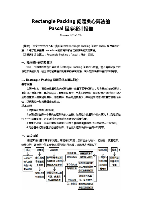
三. 需求分析根据算法的基本需求和流程,用程序实现时,总体应分为输入、初始化、放置矩形、结果分析、输出五个基本步骤来对问题进行求解,其流程方框图如下:四. 用Pascal实现Rectangle Packing问题的贪心算法1. 程序定义的主要的数组型变量:w,h:array [1..300] of integer; {width and height of each rectangles}used:array [1..300] of boolean; {Hash table for used rectangles}state:array [1..300,1..4] of integer; {location of put rectangles}legalpos:array [1..10000,1..7] of integer; {legal position of newly put rectangle} dmin:array [1..10000] of integer; {min distance of put rectangle and others} c:array [1..10000] of real; {caving degree of each rectangles}c1:array [1..1000] of integer; {rectangles of 1 caving degree} cornercheck:array [1..4,1..2] of boolean; {Hash table for occupied corners} corners:array [1..300] of integer; {occupied corners of each coa}2. 程序中主要的procedure的作用:procedure init “输入”——用于读入容器和各个矩形的长宽。
MIPS芯片架构说明
MIPS32™ Architecture For Programmers Volume I: Introduction to the MIPS32™ArchitectureDocument Number: MD00082Revision 2.00June 8, 2003MIPS Technologies, Inc.1225 Charleston RoadMountain View, CA 94043-1353Copyright © 2001-2003 MIPS Technologies Inc. All rights reserved.Copyright ©2001-2003 MIPS Technologies, Inc. All rights reserved.Unpublished rights (if any) reserved under the copyright laws of the United States of America and other countries.This document contains information that is proprietary to MIPS Technologies, Inc. ("MIPS Technologies"). Any copying,reproducing,modifying or use of this information(in whole or in part)that is not expressly permitted in writing by MIPS Technologies or an authorized third party is strictly prohibited. At a minimum, this information is protected under unfair competition and copyright laws. Violations thereof may result in criminal penalties and fines.Any document provided in source format(i.e.,in a modifiable form such as in FrameMaker or Microsoft Word format) is subject to use and distribution restrictions that are independent of and supplemental to any and all confidentiality restrictions. UNDER NO CIRCUMSTANCES MAY A DOCUMENT PROVIDED IN SOURCE FORMAT BE DISTRIBUTED TO A THIRD PARTY IN SOURCE FORMAT WITHOUT THE EXPRESS WRITTEN PERMISSION OF MIPS TECHNOLOGIES, INC.MIPS Technologies reserves the right to change the information contained in this document to improve function,design or otherwise.MIPS Technologies does not assume any liability arising out of the application or use of this information, or of any error or omission in such information. Any warranties, whether express, statutory, implied or otherwise, including but not limited to the implied warranties of merchantability orfitness for a particular purpose,are excluded. Except as expressly provided in any written license agreement from MIPS Technologies or an authorized third party,the furnishing of this document does not give recipient any license to any intellectual property rights,including any patent rights, that cover the information in this document.The information contained in this document shall not be exported or transferred for the purpose of reexporting in violation of any U.S. or non-U.S. regulation, treaty, Executive Order, law, statute, amendment or supplement thereto. The information contained in this document constitutes one or more of the following: commercial computer software, commercial computer software documentation or other commercial items.If the user of this information,or any related documentation of any kind,including related technical data or manuals,is an agency,department,or other entity of the United States government ("Government"), the use, duplication, reproduction, release, modification, disclosure, or transfer of this information, or any related documentation of any kind, is restricted in accordance with Federal Acquisition Regulation12.212for civilian agencies and Defense Federal Acquisition Regulation Supplement227.7202 for military agencies.The use of this information by the Government is further restricted in accordance with the terms of the license agreement(s) and/or applicable contract terms and conditions covering this information from MIPS Technologies or an authorized third party.MIPS,R3000,R4000,R5000and R10000are among the registered trademarks of MIPS Technologies,Inc.in the United States and other countries,and MIPS16,MIPS16e,MIPS32,MIPS64,MIPS-3D,MIPS-based,MIPS I,MIPS II,MIPS III,MIPS IV,MIPS V,MIPSsim,SmartMIPS,MIPS Technologies logo,4K,4Kc,4Km,4Kp,4KE,4KEc,4KEm,4KEp, 4KS, 4KSc, 4KSd, M4K, 5K, 5Kc, 5Kf, 20Kc, 25Kf, ASMACRO, ATLAS, At the Core of the User Experience., BusBridge, CoreFPGA, CoreLV, EC, JALGO, MALTA, MDMX, MGB, PDtrace, Pipeline, Pro, Pro Series, SEAD, SEAD-2, SOC-it and YAMON are among the trademarks of MIPS Technologies, Inc.All other trademarks referred to herein are the property of their respective owners.Template: B1.08, Built with tags: 2B ARCH MIPS32MIPS32™ Architecture For Programmers Volume I, Revision 2.00 Copyright © 2001-2003 MIPS Technologies Inc. All rights reserved.Table of ContentsChapter 1 About This Book (1)1.1 Typographical Conventions (1)1.1.1 Italic Text (1)1.1.2 Bold Text (1)1.1.3 Courier Text (1)1.2 UNPREDICTABLE and UNDEFINED (2)1.2.1 UNPREDICTABLE (2)1.2.2 UNDEFINED (2)1.3 Special Symbols in Pseudocode Notation (2)1.4 For More Information (4)Chapter 2 The MIPS Architecture: An Introduction (7)2.1 MIPS32 and MIPS64 Overview (7)2.1.1 Historical Perspective (7)2.1.2 Architectural Evolution (7)2.1.3 Architectural Changes Relative to the MIPS I through MIPS V Architectures (9)2.2 Compliance and Subsetting (9)2.3 Components of the MIPS Architecture (10)2.3.1 MIPS Instruction Set Architecture (ISA) (10)2.3.2 MIPS Privileged Resource Architecture (PRA) (10)2.3.3 MIPS Application Specific Extensions (ASEs) (10)2.3.4 MIPS User Defined Instructions (UDIs) (11)2.4 Architecture Versus Implementation (11)2.5 Relationship between the MIPS32 and MIPS64 Architectures (11)2.6 Instructions, Sorted by ISA (12)2.6.1 List of MIPS32 Instructions (12)2.6.2 List of MIPS64 Instructions (13)2.7 Pipeline Architecture (13)2.7.1 Pipeline Stages and Execution Rates (13)2.7.2 Parallel Pipeline (14)2.7.3 Superpipeline (14)2.7.4 Superscalar Pipeline (14)2.8 Load/Store Architecture (15)2.9 Programming Model (15)2.9.1 CPU Data Formats (16)2.9.2 FPU Data Formats (16)2.9.3 Coprocessors (CP0-CP3) (16)2.9.4 CPU Registers (16)2.9.5 FPU Registers (18)2.9.6 Byte Ordering and Endianness (21)2.9.7 Memory Access Types (25)2.9.8 Implementation-Specific Access Types (26)2.9.9 Cache Coherence Algorithms and Access Types (26)2.9.10 Mixing Access Types (26)Chapter 3 Application Specific Extensions (27)3.1 Description of ASEs (27)3.2 List of Application Specific Instructions (28)3.2.1 The MIPS16e Application Specific Extension to the MIPS32Architecture (28)3.2.2 The MDMX Application Specific Extension to the MIPS64 Architecture (28)3.2.3 The MIPS-3D Application Specific Extension to the MIPS64 Architecture (28)MIPS32™ Architecture For Programmers Volume I, Revision 2.00i Copyright © 2001-2003 MIPS Technologies Inc. All rights reserved.3.2.4 The SmartMIPS Application Specific Extension to the MIPS32 Architecture (28)Chapter 4 Overview of the CPU Instruction Set (29)4.1 CPU Instructions, Grouped By Function (29)4.1.1 CPU Load and Store Instructions (29)4.1.2 Computational Instructions (32)4.1.3 Jump and Branch Instructions (35)4.1.4 Miscellaneous Instructions (37)4.1.5 Coprocessor Instructions (40)4.2 CPU Instruction Formats (41)Chapter 5 Overview of the FPU Instruction Set (43)5.1 Binary Compatibility (43)5.2 Enabling the Floating Point Coprocessor (44)5.3 IEEE Standard 754 (44)5.4 FPU Data Types (44)5.4.1 Floating Point Formats (44)5.4.2 Fixed Point Formats (48)5.5 Floating Point Register Types (48)5.5.1 FPU Register Models (49)5.5.2 Binary Data Transfers (32-Bit and 64-Bit) (49)5.5.3 FPRs and Formatted Operand Layout (50)5.6 Floating Point Control Registers (FCRs) (50)5.6.1 Floating Point Implementation Register (FIR, CP1 Control Register 0) (51)5.6.2 Floating Point Control and Status Register (FCSR, CP1 Control Register 31) (53)5.6.3 Floating Point Condition Codes Register (FCCR, CP1 Control Register 25) (55)5.6.4 Floating Point Exceptions Register (FEXR, CP1 Control Register 26) (56)5.6.5 Floating Point Enables Register (FENR, CP1 Control Register 28) (56)5.7 Formats of Values Used in FP Registers (57)5.8 FPU Exceptions (58)5.8.1 Exception Conditions (59)5.9 FPU Instructions (62)5.9.1 Data Transfer Instructions (62)5.9.2 Arithmetic Instructions (63)5.9.3 Conversion Instructions (65)5.9.4 Formatted Operand-Value Move Instructions (66)5.9.5 Conditional Branch Instructions (67)5.9.6 Miscellaneous Instructions (68)5.10 Valid Operands for FPU Instructions (68)5.11 FPU Instruction Formats (70)5.11.1 Implementation Note (71)Appendix A Instruction Bit Encodings (75)A.1 Instruction Encodings and Instruction Classes (75)A.2 Instruction Bit Encoding Tables (75)A.3 Floating Point Unit Instruction Format Encodings (82)Appendix B Revision History (85)ii MIPS32™ Architecture For Programmers Volume I, Revision 2.00 Copyright © 2001-2003 MIPS Technologies Inc. All rights reserved.Figure 2-1: Relationship between the MIPS32 and MIPS64 Architectures (11)Figure 2-2: One-Deep Single-Completion Instruction Pipeline (13)Figure 2-3: Four-Deep Single-Completion Pipeline (14)Figure 2-4: Four-Deep Superpipeline (14)Figure 2-5: Four-Way Superscalar Pipeline (15)Figure 2-6: CPU Registers (18)Figure 2-7: FPU Registers for a 32-bit FPU (20)Figure 2-8: FPU Registers for a 64-bit FPU if Status FR is 1 (21)Figure 2-9: FPU Registers for a 64-bit FPU if Status FR is 0 (22)Figure 2-10: Big-Endian Byte Ordering (23)Figure 2-11: Little-Endian Byte Ordering (23)Figure 2-12: Big-Endian Data in Doubleword Format (24)Figure 2-13: Little-Endian Data in Doubleword Format (24)Figure 2-14: Big-Endian Misaligned Word Addressing (25)Figure 2-15: Little-Endian Misaligned Word Addressing (25)Figure 3-1: MIPS ISAs and ASEs (27)Figure 3-2: User-Mode MIPS ISAs and Optional ASEs (27)Figure 4-1: Immediate (I-Type) CPU Instruction Format (42)Figure 4-2: Jump (J-Type) CPU Instruction Format (42)Figure 4-3: Register (R-Type) CPU Instruction Format (42)Figure 5-1: Single-Precisions Floating Point Format (S) (45)Figure 5-2: Double-Precisions Floating Point Format (D) (45)Figure 5-3: Paired Single Floating Point Format (PS) (46)Figure 5-4: Word Fixed Point Format (W) (48)Figure 5-5: Longword Fixed Point Format (L) (48)Figure 5-6: FPU Word Load and Move-to Operations (49)Figure 5-7: FPU Doubleword Load and Move-to Operations (50)Figure 5-8: Single Floating Point or Word Fixed Point Operand in an FPR (50)Figure 5-9: Double Floating Point or Longword Fixed Point Operand in an FPR (50)Figure 5-10: Paired-Single Floating Point Operand in an FPR (50)Figure 5-11: FIR Register Format (51)Figure 5-12: FCSR Register Format (53)Figure 5-13: FCCR Register Format (55)Figure 5-14: FEXR Register Format (56)Figure 5-15: FENR Register Format (56)Figure 5-16: Effect of FPU Operations on the Format of Values Held in FPRs (58)Figure 5-17: I-Type (Immediate) FPU Instruction Format (71)Figure 5-18: R-Type (Register) FPU Instruction Format (71)Figure 5-19: Register-Immediate FPU Instruction Format (71)Figure 5-20: Condition Code, Immediate FPU Instruction Format (71)Figure 5-21: Formatted FPU Compare Instruction Format (71)Figure 5-22: FP RegisterMove, Conditional Instruction Format (71)Figure 5-23: Four-Register Formatted Arithmetic FPU Instruction Format (72)Figure 5-24: Register Index FPU Instruction Format (72)Figure 5-25: Register Index Hint FPU Instruction Format (72)Figure 5-26: Condition Code, Register Integer FPU Instruction Format (72)Figure A-1: Sample Bit Encoding Table (76)MIPS32™ Architecture For Programmers Volume I, Revision 2.00iii Copyright © 2001-2003 MIPS Technologies Inc. All rights reserved.Table 1-1: Symbols Used in Instruction Operation Statements (2)Table 2-1: MIPS32 Instructions (12)Table 2-2: MIPS64 Instructions (13)Table 2-3: Unaligned Load and Store Instructions (24)Table 4-1: Load and Store Operations Using Register + Offset Addressing Mode (30)Table 4-2: Aligned CPU Load/Store Instructions (30)Table 4-3: Unaligned CPU Load and Store Instructions (31)Table 4-4: Atomic Update CPU Load and Store Instructions (31)Table 4-5: Coprocessor Load and Store Instructions (31)Table 4-6: FPU Load and Store Instructions Using Register+Register Addressing (32)Table 4-7: ALU Instructions With an Immediate Operand (33)Table 4-8: Three-Operand ALU Instructions (33)Table 4-9: Two-Operand ALU Instructions (34)Table 4-10: Shift Instructions (34)Table 4-11: Multiply/Divide Instructions (35)Table 4-12: Unconditional Jump Within a 256 Megabyte Region (36)Table 4-13: PC-Relative Conditional Branch Instructions Comparing Two Registers (36)Table 4-14: PC-Relative Conditional Branch Instructions Comparing With Zero (37)Table 4-15: Deprecated Branch Likely Instructions (37)Table 4-16: Serialization Instruction (38)Table 4-17: System Call and Breakpoint Instructions (38)Table 4-18: Trap-on-Condition Instructions Comparing Two Registers (38)Table 4-19: Trap-on-Condition Instructions Comparing an Immediate Value (38)Table 4-20: CPU Conditional Move Instructions (39)Table 4-21: Prefetch Instructions (39)Table 4-22: NOP Instructions (40)Table 4-23: Coprocessor Definition and Use in the MIPS Architecture (40)Table 4-24: CPU Instruction Format Fields (42)Table 5-1: Parameters of Floating Point Data Types (45)Table 5-2: Value of Single or Double Floating Point DataType Encoding (46)Table 5-3: Value Supplied When a New Quiet NaN Is Created (47)Table 5-4: FIR Register Field Descriptions (51)Table 5-5: FCSR Register Field Descriptions (53)Table 5-6: Cause, Enable, and Flag Bit Definitions (55)Table 5-7: Rounding Mode Definitions (55)Table 5-8: FCCR Register Field Descriptions (56)Table 5-9: FEXR Register Field Descriptions (56)Table 5-10: FENR Register Field Descriptions (57)Table 5-11: Default Result for IEEE Exceptions Not Trapped Precisely (60)Table 5-12: FPU Data Transfer Instructions (62)Table 5-13: FPU Loads and Stores Using Register+Offset Address Mode (63)Table 5-14: FPU Loads and Using Register+Register Address Mode (63)Table 5-15: FPU Move To and From Instructions (63)Table 5-16: FPU IEEE Arithmetic Operations (64)Table 5-17: FPU-Approximate Arithmetic Operations (64)Table 5-18: FPU Multiply-Accumulate Arithmetic Operations (65)Table 5-19: FPU Conversion Operations Using the FCSR Rounding Mode (65)Table 5-20: FPU Conversion Operations Using a Directed Rounding Mode (65)Table 5-21: FPU Formatted Operand Move Instructions (66)Table 5-22: FPU Conditional Move on True/False Instructions (66)iv MIPS32™ Architecture For Programmers Volume I, Revision 2.00 Copyright © 2001-2003 MIPS Technologies Inc. All rights reserved.Table 5-23: FPU Conditional Move on Zero/Nonzero Instructions (67)Table 5-24: FPU Conditional Branch Instructions (67)Table 5-25: Deprecated FPU Conditional Branch Likely Instructions (67)Table 5-26: CPU Conditional Move on FPU True/False Instructions (68)Table 5-27: FPU Operand Format Field (fmt, fmt3) Encoding (68)Table 5-28: Valid Formats for FPU Operations (69)Table 5-29: FPU Instruction Format Fields (72)Table A-1: Symbols Used in the Instruction Encoding Tables (76)Table A-2: MIPS32 Encoding of the Opcode Field (77)Table A-3: MIPS32 SPECIAL Opcode Encoding of Function Field (78)Table A-4: MIPS32 REGIMM Encoding of rt Field (78)Table A-5: MIPS32 SPECIAL2 Encoding of Function Field (78)Table A-6: MIPS32 SPECIAL3 Encoding of Function Field for Release 2 of the Architecture (78)Table A-7: MIPS32 MOVCI Encoding of tf Bit (79)Table A-8: MIPS32 SRL Encoding of Shift/Rotate (79)Table A-9: MIPS32 SRLV Encoding of Shift/Rotate (79)Table A-10: MIPS32 BSHFL Encoding of sa Field (79)Table A-11: MIPS32 COP0 Encoding of rs Field (79)Table A-12: MIPS32 COP0 Encoding of Function Field When rs=CO (80)Table A-13: MIPS32 COP1 Encoding of rs Field (80)Table A-14: MIPS32 COP1 Encoding of Function Field When rs=S (80)Table A-15: MIPS32 COP1 Encoding of Function Field When rs=D (81)Table A-16: MIPS32 COP1 Encoding of Function Field When rs=W or L (81)Table A-17: MIPS64 COP1 Encoding of Function Field When rs=PS (81)Table A-18: MIPS32 COP1 Encoding of tf Bit When rs=S, D, or PS, Function=MOVCF (81)Table A-19: MIPS32 COP2 Encoding of rs Field (82)Table A-20: MIPS64 COP1X Encoding of Function Field (82)Table A-21: Floating Point Unit Instruction Format Encodings (82)MIPS32™ Architecture For Programmers Volume I, Revision 2.00v Copyright © 2001-2003 MIPS Technologies Inc. All rights reserved.vi MIPS32™ Architecture For Programmers Volume I, Revision 2.00 Copyright © 2001-2003 MIPS Technologies Inc. All rights reserved.Chapter 1About This BookThe MIPS32™ Architecture For Programmers V olume I comes as a multi-volume set.•V olume I describes conventions used throughout the document set, and provides an introduction to the MIPS32™Architecture•V olume II provides detailed descriptions of each instruction in the MIPS32™ instruction set•V olume III describes the MIPS32™Privileged Resource Architecture which defines and governs the behavior of the privileged resources included in a MIPS32™ processor implementation•V olume IV-a describes the MIPS16e™ Application-Specific Extension to the MIPS32™ Architecture•V olume IV-b describes the MDMX™ Application-Specific Extension to the MIPS32™ Architecture and is notapplicable to the MIPS32™ document set•V olume IV-c describes the MIPS-3D™ Application-Specific Extension to the MIPS64™ Architecture and is notapplicable to the MIPS32™ document set•V olume IV-d describes the SmartMIPS™Application-Specific Extension to the MIPS32™ Architecture1.1Typographical ConventionsThis section describes the use of italic,bold and courier fonts in this book.1.1.1Italic Text•is used for emphasis•is used for bits,fields,registers, that are important from a software perspective (for instance, address bits used bysoftware,and programmablefields and registers),and variousfloating point instruction formats,such as S,D,and PS •is used for the memory access types, such as cached and uncached1.1.2Bold Text•represents a term that is being defined•is used for bits andfields that are important from a hardware perspective (for instance,register bits, which are not programmable but accessible only to hardware)•is used for ranges of numbers; the range is indicated by an ellipsis. For instance,5..1indicates numbers 5 through 1•is used to emphasize UNPREDICTABLE and UNDEFINED behavior, as defined below.1.1.3Courier TextCourier fixed-width font is used for text that is displayed on the screen, and for examples of code and instruction pseudocode.MIPS32™ Architecture For Programmers Volume I, Revision 2.001 Copyright © 2001-2003 MIPS Technologies Inc. All rights reserved.Chapter 1 About This Book1.2UNPREDICTABLE and UNDEFINEDThe terms UNPREDICTABLE and UNDEFINED are used throughout this book to describe the behavior of theprocessor in certain cases.UNDEFINED behavior or operations can occur only as the result of executing instructions in a privileged mode (i.e., in Kernel Mode or Debug Mode, or with the CP0 usable bit set in the Status register).Unprivileged software can never cause UNDEFINED behavior or operations. Conversely, both privileged andunprivileged software can cause UNPREDICTABLE results or operations.1.2.1UNPREDICTABLEUNPREDICTABLE results may vary from processor implementation to implementation,instruction to instruction,or as a function of time on the same implementation or instruction. Software can never depend on results that areUNPREDICTABLE.UNPREDICTABLE operations may cause a result to be generated or not.If a result is generated, it is UNPREDICTABLE.UNPREDICTABLE operations may cause arbitrary exceptions.UNPREDICTABLE results or operations have several implementation restrictions:•Implementations of operations generating UNPREDICTABLE results must not depend on any data source(memory or internal state) which is inaccessible in the current processor mode•UNPREDICTABLE operations must not read, write, or modify the contents of memory or internal state which is inaccessible in the current processor mode. For example,UNPREDICTABLE operations executed in user modemust not access memory or internal state that is only accessible in Kernel Mode or Debug Mode or in another process •UNPREDICTABLE operations must not halt or hang the processor1.2.2UNDEFINEDUNDEFINED operations or behavior may vary from processor implementation to implementation, instruction toinstruction, or as a function of time on the same implementation or instruction.UNDEFINED operations or behavior may vary from nothing to creating an environment in which execution can no longer continue.UNDEFINED operations or behavior may cause data loss.UNDEFINED operations or behavior has one implementation restriction:•UNDEFINED operations or behavior must not cause the processor to hang(that is,enter a state from which there is no exit other than powering down the processor).The assertion of any of the reset signals must restore the processor to an operational state1.3Special Symbols in Pseudocode NotationIn this book, algorithmic descriptions of an operation are described as pseudocode in a high-level language notation resembling Pascal. Special symbols used in the pseudocode notation are listed in Table 1-1.Table 1-1 Symbols Used in Instruction Operation StatementsSymbol Meaning←Assignment=, ≠Tests for equality and inequality||Bit string concatenationx y A y-bit string formed by y copies of the single-bit value x2MIPS32™ Architecture For Programmers Volume I, Revision 2.00 Copyright © 2001-2003 MIPS Technologies Inc. All rights reserved.1.3Special Symbols in Pseudocode Notationb#n A constant value n in base b.For instance10#100represents the decimal value100,2#100represents the binary value 100 (decimal 4), and 16#100 represents the hexadecimal value 100 (decimal 256). If the "b#" prefix is omitted, the default base is 10.x y..z Selection of bits y through z of bit string x.Little-endian bit notation(rightmost bit is0)is used.If y is less than z, this expression is an empty (zero length) bit string.+, −2’s complement or floating point arithmetic: addition, subtraction∗, ×2’s complement or floating point multiplication (both used for either)div2’s complement integer divisionmod2’s complement modulo/Floating point division<2’s complement less-than comparison>2’s complement greater-than comparison≤2’s complement less-than or equal comparison≥2’s complement greater-than or equal comparisonnor Bitwise logical NORxor Bitwise logical XORand Bitwise logical ANDor Bitwise logical ORGPRLEN The length in bits (32 or 64) of the CPU general-purpose registersGPR[x]CPU general-purpose register x. The content of GPR[0] is always zero.SGPR[s,x]In Release 2 of the Architecture, multiple copies of the CPU general-purpose registers may be implemented.SGPR[s,x] refers to GPR set s, register x. GPR[x] is a short-hand notation for SGPR[ SRSCtl CSS, x].FPR[x]Floating Point operand register xFCC[CC]Floating Point condition code CC.FCC[0] has the same value as COC[1].FPR[x]Floating Point (Coprocessor unit 1), general register xCPR[z,x,s]Coprocessor unit z, general register x,select sCP2CPR[x]Coprocessor unit 2, general register xCCR[z,x]Coprocessor unit z, control register xCP2CCR[x]Coprocessor unit 2, control register xCOC[z]Coprocessor unit z condition signalXlat[x]Translation of the MIPS16e GPR number x into the corresponding 32-bit GPR numberBigEndianMem Endian mode as configured at chip reset (0→Little-Endian, 1→ Big-Endian). Specifies the endianness of the memory interface(see LoadMemory and StoreMemory pseudocode function descriptions),and the endianness of Kernel and Supervisor mode execution.BigEndianCPU The endianness for load and store instructions (0→ Little-Endian, 1→ Big-Endian). In User mode, this endianness may be switched by setting the RE bit in the Status register.Thus,BigEndianCPU may be computed as (BigEndianMem XOR ReverseEndian).Table 1-1 Symbols Used in Instruction Operation StatementsSymbol MeaningChapter 1 About This Book1.4For More InformationVarious MIPS RISC processor manuals and additional information about MIPS products can be found at the MIPS URL:ReverseEndianSignal to reverse the endianness of load and store instructions.This feature is available in User mode only,and is implemented by setting the RE bit of the Status register.Thus,ReverseEndian may be computed as (SR RE and User mode).LLbitBit of virtual state used to specify operation for instructions that provide atomic read-modify-write.LLbit is set when a linked load occurs; it is tested and cleared by the conditional store. It is cleared, during other CPU operation,when a store to the location would no longer be atomic.In particular,it is cleared by exception return instructions.I :,I+n :,I-n :This occurs as a prefix to Operation description lines and functions as a label. It indicates the instruction time during which the pseudocode appears to “execute.” Unless otherwise indicated, all effects of the currentinstruction appear to occur during the instruction time of the current instruction.No label is equivalent to a time label of I . Sometimes effects of an instruction appear to occur either earlier or later — that is, during theinstruction time of another instruction.When this happens,the instruction operation is written in sections labeled with the instruction time,relative to the current instruction I ,in which the effect of that pseudocode appears to occur.For example,an instruction may have a result that is not available until after the next instruction.Such an instruction has the portion of the instruction operation description that writes the result register in a section labeled I +1.The effect of pseudocode statements for the current instruction labelled I +1appears to occur “at the same time”as the effect of pseudocode statements labeled I for the following instruction.Within one pseudocode sequence,the effects of the statements take place in order. However, between sequences of statements for differentinstructions that occur “at the same time,” there is no defined order. Programs must not depend on a particular order of evaluation between such sections.PCThe Program Counter value.During the instruction time of an instruction,this is the address of the instruction word. The address of the instruction that occurs during the next instruction time is determined by assigning a value to PC during an instruction time. If no value is assigned to PC during an instruction time by anypseudocode statement,it is automatically incremented by either 2(in the case of a 16-bit MIPS16e instruction)or 4before the next instruction time.A taken branch assigns the target address to the PC during the instruction time of the instruction in the branch delay slot.PABITSThe number of physical address bits implemented is represented by the symbol PABITS.As such,if 36physical address bits were implemented, the size of the physical address space would be 2PABITS = 236 bytes.FP32RegistersModeIndicates whether the FPU has 32-bit or 64-bit floating point registers (FPRs).In MIPS32,the FPU has 3232-bit FPRs in which 64-bit data types are stored in even-odd pairs of FPRs.In MIPS64,the FPU has 3264-bit FPRs in which 64-bit data types are stored in any FPR.In MIPS32implementations,FP32RegistersMode is always a 0.MIPS64implementations have a compatibility mode in which the processor references the FPRs as if it were a MIPS32 implementation. In such a caseFP32RegisterMode is computed from the FR bit in the Status register.If this bit is a 0,the processor operates as if it had 32 32-bit FPRs. If this bit is a 1, the processor operates with 32 64-bit FPRs.The value of FP32RegistersMode is computed from the FR bit in the Status register.InstructionInBranchDelaySlotIndicates whether the instruction at the Program Counter address was executed in the delay slot of a branch or jump. This condition reflects the dynamic state of the instruction, not the static state. That is, the value is false if a branch or jump occurs to an instruction whose PC immediately follows a branch or jump, but which is not executed in the delay slot of a branch or jump.SignalException(exce ption, argument)Causes an exception to be signaled, using the exception parameter as the type of exception and the argument parameter as an exception-specific argument). Control does not return from this pseudocode function - the exception is signaled at the point of the call.Table 1-1 Symbols Used in Instruction Operation StatementsSymbolMeaning。
Unit5 packaging物流专业英语 包装讲课稿

Dialogue 1 Packing of Silk
Stocking
Smith:Good .A wrapping that catches the eye will certainly help push sales. With keen competition from similar silk stocking producers, the merchandise must not only be of nice quality, but also look attractive.
Lin:Right. We'll see to it that the silk stockings appeal to the eye as well as to the purse.
Smith:What about the outer packing?
Dialogue 1 Packing of Silk
Text 1 Introduction of Packaging
New Words and Phrases
withstand appealing significance widespread insufficient confuse
v. 抵抗,经受住 adj. 吸引人的
n. 意义,重要性 adj.分布广泛的,普遍的 adj.不足的,不够的
Smith:What are your conditions, Mr. Lin, as far as packaging is concerned?
Lin:Well, as you know, we have definite ways of packing silk stockings for sea shipment. As a rule, we use polythene wrapper for each article, all ready for shelf selling.
求解圆形packing问题的一个启发式算法

求解圆形packing问题的一个启发式算法
圆形packing问题,即将一定数量的圆形在最小的矩形空间内放置,一直困扰着十分谨慎的研究者们。
为了优化该问题的处理,应始终采用最少排列多边形空间中最大半径的圆形,在边缘放置最小半径的圆形,以便将最大量的圆形放入有限的空间。
为了解决这一概念,研究者们提出了一个称为启发式算法的概念。
该算法是基于模拟退火法的,即从大量的基于统计和无穷小的基于知识的搜索方法中利用一个启发式的方法,比如随机搜索或者策略搜索等来改善这种排列,之后根据参数和约束条件来进行调整,以达到放置最多圆形所需要的最小底面积。
启发式算法可以将空间划分为若干个网格,按照其中预定义的规则,对圆形进行摆放,比如用于放置最大半径的圆形,具体放置在指定的位置,在接下来的步骤中可以依据该放置位置逐步插入较小的圆形。
此外,还可以通过算法构建一个计算多边形面积的模型,通过不断的迭代圆形的放置位置使多边形的面积最大程度的减小。
经过对该问题的深入研究及改进,启发式算法已成为当前研究的行之有效的方法,在求解圆形packing问题方面发挥着不可忽视的作用。
许多研究者结合该算法与其他辅助技术,如粒子群算法、遗传算法等,以提高该算法的精度和收敛性,保证该算法求解圆形packing问题的效果。
- 1、下载文档前请自行甄别文档内容的完整性,平台不提供额外的编辑、内容补充、找答案等附加服务。
- 2、"仅部分预览"的文档,不可在线预览部分如存在完整性等问题,可反馈申请退款(可完整预览的文档不适用该条件!)。
- 3、如文档侵犯您的权益,请联系客服反馈,我们会尽快为您处理(人工客服工作时间:9:00-18:30)。
USACO 1.4.1 Packing Rectangles
Packing Rectangles
IOI 95
The six basic layouts of four rectangles
Four rectangles are given. Find the smallest enclosing (new) rectangle into which these four may be fitted without overlapping. By smallest rectangle, we mean the one with the smallest area.
All four rectangles should have their sides parallel to the corresponding sides of the enclosing rectangle. Figure 1 shows six ways to fit four rectangles together. These six are the only possible basic layouts, since any other layout can be obtained from a basic layout by rotation or reflection. Rectangles may be rotated 90 degrees during packing.
There may exist several different enclosing rectangles fulfilling the requirements, all with the same area. Y ou must produce all such enclosing rectangles.
PROGRAM NAME: packrec
INPUT FORMA T
Four lines, each containing two positive space-separated integers that represent the lengths of a rectangle's two sides. Each side of a rectangle is at least 1 and at most 50.
SAMPLE INPUT (file packrec.in)
1 2
2 3
3 4
4 5
OUTPUT FORMA T
The output file contains one line more than the number of solutions. The first line contains a single integer: the minimum area of the enclosing rectangles. Each of the following lines contains one solution described by two numbers p and q with p<=q. These lines must be sorted in ascending order of p, and must all be different.
SAMPLE OUTPUT (file packrec.out)
40
4 10
5 8
Packing Rectangles
铺放矩形块
IOI 95
译by leontea
给定4个矩形块,找出一个最小的封闭矩形将这4个矩形块放入,但不得相互重叠。
所谓最小矩形指该矩形面积最小。
所有4个矩形块的边都与封闭矩形的边相平行,图1示出了铺放4个矩形块的6种方案。
这6种方案仅只是可能的基本铺放方案。
因为其它方案能由基本方案通过旋转和镜像反射得到。
可能存在满足条件且有着同样面积的各种不同的封闭矩形,你应该输出所有这些封闭矩形的边长。
PROGRAM NAME: packrec
INPUT FORMA T
共有4行。
每一行用两个正整数来表示一个给定的矩形块的两个边长。
矩形块的每条边的边长范围最小是1,最大是50。
SAMPLE INPUT (file packrec.in)
1 2
2 3
3 4
4 5
OUTPUT FORMA T
总行数为解的总数加1。
第一行是一个整数,代表封闭矩形的最小面积(子任务A)。
接下来的每一行都表示一个解,由数P和数Q来表示,并且P≤Q(子任务B)。
这些行必须根据P的大小按升序排列,P小的行在前,大的在后。
且所有行都应是不同的。
SAMPLE OUTPUT (file packrec.out)
40
4 10
5 8。