MAX6380_R34-T中文资料
MAX832中文资料
NUAL KIT MA ATION U EET L H A S V A E T WS DA FOLLO
___________________________Features
o Input Range: Up to 30V o 1A On-Chip Power Switch o Adjustable Output (MAX830) Fixed Outputs: 5V (MAX831) 3.3V (MAX832) 3V (MAX833) o 100kHz Switching Frequency o Excellent Dynamic Characteristics o Few External Components o 8mA Quiescent Current o 16-Pin SO Package o Evaluation Kit Available
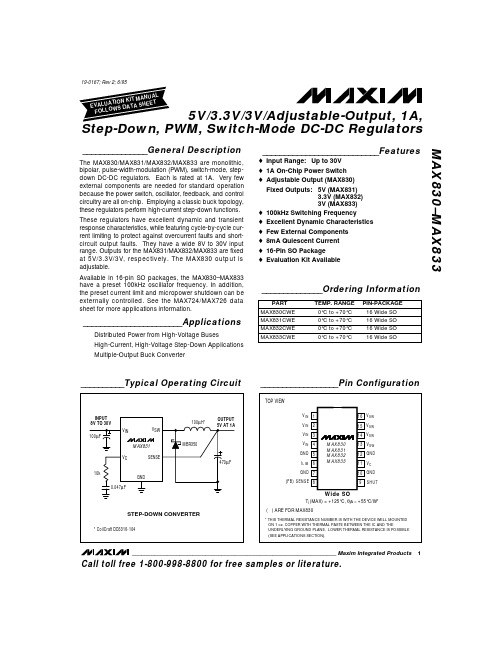
__________Typical Operating Circuit
__________________Pin Configuration
TOP VIEW
INPUT 8V TO 30V 100µF VIN VSW
100µH*
OUTPUT 5V AT 1A
V IN 1 V IN 2 V IN 3
16 V SW 15 V SW 14 V SW
_______________________Applications
Distributed Power from High-Voltage Buses High-Current, High-Voltage Step-Down Applications Multiple-Output Buck Converter
MAX831
VC 10k 0.047µF SENSE
MAX13085EESA-T中文资料

General DescriptionThe MAX13080E–MAX13089E +5.0V, ±15kV ESD-protect-ed, RS-485/RS-422 transceivers feature one driver and one receiver. These devices include fail-safe circuitry,guaranteeing a logic-high receiver output when receiver inputs are open or shorted. The receiver outputs a logic-high if all transmitters on a terminated bus are disabled (high impedance). The MAX13080E–MAX13089E include a hot-swap capability to eliminate false transitions on the bus during power-up or hot insertion.The MAX13080E/MAX13081E/MAX13082E feature reduced slew-rate drivers that minimize EMI and reduce reflections caused by improperly terminated cables, allowing error-free data transmission up to 250kbps. The MAX13083E/MAX13084E/MAX13085E also feature slew-rate-limited drivers but allow transmit speeds up to 500kbps. The MAX13086E/MAX13087E/MAX13088E driver slew rates are not limited, making transmit speeds up to 16Mbps possible. The MAX13089E slew rate is pin selectable for 250kbps,500kbps, and 16Mbps.The MAX13082E/MAX13085E/MAX13088E are intended for half-duplex communications, and the MAX13080E/MAX13081E/MAX13083E/MAX13084E/MAX13086E/MAX13087E are intended for full-duplex communica-tions. The MAX13089E is selectable for half-duplex or full-duplex operation. It also features independently programmable receiver and transmitter output phase through separate pins.The MAX13080E–MAX13089E transceivers draw 1.2mA of supply current when unloaded or when fully loaded with the drivers disabled. All devices have a 1/8-unit load receiver input impedance, allowing up to 256transceivers on the bus.The MAX13080E/MAX13083E/MAX13086E/MAX13089E are available in 14-pin PDIP and 14-pin SO packages.The MAX13081E/MAX13082E/MAX13084E/MAX13085E/MAX13087E/MAX13088E are available in 8-pin PDIP and 8-pin SO packages. The devices operate over the com-mercial, extended, and automotive temperature ranges.ApplicationsUtility Meters Lighting Systems Industrial Control Telecom Security Systems Instrumentation ProfibusFeatures♦+5.0V Operation♦Extended ESD Protection for RS-485/RS-422 I/O Pins±15kV Human Body Model ♦True Fail-Safe Receiver While Maintaining EIA/TIA-485 Compatibility ♦Hot-Swap Input Structures on DE and RE ♦Enhanced Slew-Rate Limiting Facilitates Error-Free Data Transmission(MAX13080E–MAX13085E/MAX13089E)♦Low-Current Shutdown Mode (Except MAX13081E/MAX13084E/MAX13087E)♦Pin-Selectable Full-/Half-Duplex Operation (MAX13089E)♦Phase Controls to Correct for Twisted-Pair Reversal (MAX13089E)♦Allow Up to 256 Transceivers on the Bus ♦Available in Industry-Standard 8-Pin SO PackageMAX13080E–MAX13089E+5.0V , ±15kV ESD-Protected, Fail-Safe, Hot-Swap, RS-485/RS-422 Transceivers________________________________________________________________Maxim Integrated Products 1Ordering Information19-3590; Rev 1; 4/05For pricing, delivery, and ordering information,please contact Maxim/Dallas Direct!at 1-888-629-4642, or visit Maxim’s website at .Selector Guide, Pin Configurations, and Typical Operating Circuits appear at end of data sheet.Ordering Information continued at end of data sheet.M A X 13080E –M A X 13089E+5.0V , ±15kV ESD-Protected, Fail-Safe, Hot-Swap, RS-485/RS-422 Transceivers 2_______________________________________________________________________________________ABSOLUTE MAXIMUM RATINGSDC ELECTRICAL CHARACTERISTICS(V CC = +5.0V ±10%, T A = T MIN to T MAX , unless otherwise noted. Typical values are at V CC = +5.0V and T A = +25°C.) (Note 1)Stresses beyond those listed under “Absolute Maximum Ratings” may cause permanent damage to the device. These are stress ratings only, and functional operation of the device at these or any other conditions beyond those indicated in the operational sections of the specifications is not implied. Exposure to absolute maximum rating conditions for extended periods may affect device reliability.(All Voltages Referenced to GND)Supply Voltage (V CC ).............................................................+6V Control Input Voltage (RE , DE, SLR,H/F , TXP, RXP)......................................................-0.3V to +6V Driver Input Voltage (DI)...........................................-0.3V to +6V Driver Output Voltage (Z, Y, A, B).............................-8V to +13V Receiver Input Voltage (A, B)....................................-8V to +13V Receiver Input VoltageFull Duplex (A, B)..................................................-8V to +13V Receiver Output Voltage (RO)....................-0.3V to (V CC + 0.3V)Driver Output Current.....................................................±250mAContinuous Power Dissipation (T A = +70°C)8-Pin SO (derate 5.88mW/°C above +70°C).................471mW 8-Pin Plastic DIP (derate 9.09mW/°C above +70°C).....727mW 14-Pin SO (derate 8.33mW/°C above +70°C)...............667mW 14-Pin Plastic DIP (derate 10.0mW/°C above +70°C)...800mW Operating Temperature RangesMAX1308_EC_ _.................................................0°C to +75°C MAX1308_EE_ _..............................................-40°C to +85°C MAX1308_EA_ _............................................-40°C to +125°C Junction Temperature......................................................+150°C Storage Temperature Range.............................-65°C to +150°C Lead Temperature (soldering, 10s).................................+300°CMAX13080E–MAX13089E+5.0V , ±15kV ESD-Protected, Fail-Safe, Hot-Swap, RS-485/RS-422 Transceivers_______________________________________________________________________________________3DC ELECTRICAL CHARACTERISTICS (continued)(V CC = +5.0V ±10%, T A = T MIN to T MAX , unless otherwise noted. Typical values are at V CC = +5.0V and T A = +25°C.) (Note 1)M A X 13080E –M A X 13089E+5.0V , ±15kV ESD-Protected, Fail-Safe, Hot-Swap, RS-485/RS-422 Transceivers 4_______________________________________________________________________________________DRIVER SWITCHING CHARACTERISTICSMAX13080E/MAX13081E/MAX13082E/MAX13089E WITH SRL = UNCONNECTED (250kbps)(V CC = +5.0V ±10%, T A = T MIN to T MAX , unless otherwise noted. Typical values are at V CC = +5.0V and T A = +25°C.)RECEIVER SWITCHING CHARACTERISTICSMAX13080E/MAX13081E/MAX13082E/MAX13089E WITH SRL = UNCONNECTED (250kbps)(V CC = +5.0V ±10%, T A = T MIN to T MAX , unless otherwise noted. Typical values are at V CC = +5.0V and T A = +25°C.)MAX13080E–MAX13089E+5.0V , ±15kV ESD-Protected, Fail-Safe, Hot-Swap, RS-485/RS-422 Transceivers_______________________________________________________________________________________5DRIVER SWITCHING CHARACTERISTICSMAX13083E/MAX13084E/MAX13085E/MAX13089E WITH SRL = V CC (500kbps)(V CC = +5.0V ±10%, T A = T MIN to T MAX , unless otherwise noted. Typical values are at V CC = +5.0V and T A = +25°C.)RECEIVER SWITCHING CHARACTERISTICSMAX13083E/MAX13084E/MAX13085E/MAX13089E WITH SRL = V CC (500kbps)(V CC = +5.0V ±10%, T A = T MIN to T MAX , unless otherwise noted. Typical values are at V CC = +5.0V and T A = +25°C.)M A X 13080E –M A X 13089E+5.0V , ±15kV ESD-Protected, Fail-Safe, Hot-Swap, RS-485/RS-422 Transceivers 6_______________________________________________________________________________________DRIVER SWITCHING CHARACTERISTICSMAX13086E/MAX13087E/MAX13088E/MAX13089E WITH SRL = GND (16Mbps)(V CC = +5.0V ±10%, T A = T MIN to T MAX , unless otherwise noted. Typical values are at V CC = +5.0V and T A = +25°C.)RECEIVER SWITCHING CHARACTERISTICSMAX13086E/MAX13087E/MAX13088E/MAX13089E WITH SRL = GND (16Mbps)(V CC = +5.0V ±10%, T A = T MIN to T MAX , unless otherwise noted. Typical values are at V CC = +5.0V and T A = +25°C.)Note 2:∆V OD and ∆V OC are the changes in V OD and V OC , respectively, when the DI input changes state.Note 3:The short-circuit output current applies to peak current just prior to foldback current limiting. The short-circuit foldback outputcurrent applies during current limiting to allow a recovery from bus contention.MAX13080E–MAX13089E+5.0V , ±15kV ESD-Protected, Fail-Safe, Hot-Swap, RS-485/RS-422 Transceivers_______________________________________________________________________________________70.800.901.501.101.001.201.301.401.60-40-10520-253550958011065125SUPPLY CURRENT vs. TEMPERATURETEMPERATURE (°C)S U P P L Y C U R R E N T (m A )0201040305060021345OUTPUT CURRENTvs. RECEIVER OUTPUT-HIGH VOLTAGEM A X 13080E -89E t o c 02OUTPUT HIGH VOLTAGE (V)O U T P U T C U R R E N T (m A )20104030605070021345OUTPUT CURRENTvs. RECEIVER OUTPUT-LOW VOLTAGEM A X 13080E -89E t o c 03OUTPUT LOW VOLTAGE (V)O U T P U T C U R R E N T (m A )4.04.44.24.84.65.25.05.4RECEIVER OUTPUT-HIGH VOLTAGEvs. TEMPERATURETEMPERATURE (°C)O U T P U T H I G H V O L T A G E (V )-40-10520-2535509580110651250.10.70.30.20.40.50.60.8RECEIVER OUTPUT-LOW VOLTAGEvs. TEMPERATURETEMPERATURE (°C)O U T P U T L O W V O L T A G E (V )-40-10520-25355095801106512502040608010012014016012345DRIVER DIFFERENTIAL OUTPUT CURRENT vs. DIFFERENTIAL OUTPUT VOLTAGEDIFFERENTIAL OUTPUT VOLTAGE (V)D I F FE R E N T I A L O U T P U T C U R R E N T (m A )2.02.82.43.63.24.44.04.8DRIVER DIFFERENTIAL OUTPUT VOLTAGE vs. TEMPERATURED I F FE R E N T I A L O U T P U T V O L T A G E (V )-40-10520-253550958011065125TEMPERATURE (°C)40201008060120140180160200-7-5-4-6-3-2-1012354OUTPUT CURRENT vs. TRANSMITTEROUTPUT-HIGH VOLTAGEOUTPUT HIGH VOLTAGE (V)O U T P U T C U R R E N T (m A )60402080100120140160180200042681012OUTPUT CURRENT vs. TRANSMITTEROUTPUT-LOW VOLTAGEOUTPUT-LOW VOLTAGE (V)O U T P U T C U R R E N T (m A )Typical Operating Characteristics(V CC = +5.0V, T A = +25°C, unless otherwise noted.)M A X 13080E –M A X 13089E+5.0V , ±15kV ESD-Protected, Fail-Safe, Hot-Swap, RS-485/RS-422 Transceivers 8_______________________________________________________________________________________21543679810SHUTDOWN CURRENT vs. TEMPERATUREM A X 13080E -89E t o c 10S H U T D O W N C U R R E N T (µA )-40-10520-253550958011065125TEMPERATURE (°C)600800700100090011001200DRIVER PROPAGATION DELAY vs. TEMPERATURE (250kbps)D R I VE R P R O P A G A T I O N D E L A Y (n s )-40-10520-253550958011065125TEMPERATURE (°C)300400350500450550600DRIVER PROPAGATION DELAY vs. TEMPERATURE (500kbps)D R I VE R P R O P A G A T I O N D E L A Y (n s )-40-10520-253550958011065125TEMPERATURE (°C)1070302040506080DRIVER PROPAGATION DELAY vs. TEMPERATURE (16Mbps)D R I VE R P R O P A G A T I O N D E L A Y (n s )-40-10520-253550958011065125TEMPERATURE (°C)40201008060120140160180RECEIVER PROPAGATION DELAYvs. TEMPERATURE (250kpbs AND 500kbps)R E C E I V E R P R O P A G A T I O N D E L A Y (n s )-40-10520-253550958011065125TEMPERATURE (°C)40201008060120140160180RECEIVER PROPAGATION DELAYvs. TEMPERATURE (16Mbps)R EC E I V E R P R O P A G AT I O N D E L A Y (n s )-40-10520-253550958011065125TEMPERATURE (°C)2µs/div DRIVER PROPAGATION DELAY (250kbps)DI 2V/divV Y - V Z 5V/divR L = 100Ω200ns/divRECEIVER PROPAGATION DELAY(250kbps AND 500kbps)V A - V B 5V/divRO 2V/divTypical Operating Characteristics (continued)(V CC = +5.0V, T A = +25°C, unless otherwise noted.)MAX13080E–MAX13089E+5.0V , ±15kV ESD-Protected, Fail-Safe, Hot-Swap, RS-485/RS-422 Transceivers_______________________________________________________________________________________9Test Circuits and Waveforms400ns/divDRIVER PROPAGATION DELAY (500kbps)DI 2V/divR L = 100ΩV Y - V Z 5V/div10ns/div DRIVER PROPAGATION DELAY (16Mbps)DI 2V/divR L = 100ΩV Y 2V/divV Z 2V/div40ns/divRECEIVER PROPAGATION DELAY (16Mbps)V B 2V/divR L = 100ΩRO 2V/divV A 2V/divTypical Operating Characteristics (continued)(V CC = +5.0V, T A = +25°C, unless otherwise noted.)Figure 2. Driver Timing Test CircuitM A X 13080E –M A X 13089E+5.0V , ±15kV ESD-Protected, Fail-Safe, Hot-Swap, RS-485/RS-422 Transceivers 10______________________________________________________________________________________Test Circuits and Waveforms (continued)Figure 4. Driver Enable and Disable Times (t DHZ , t DZH , t DZH(SHDN))DZL DLZ DLZ(SHDN)MAX13080E–MAX13089E+5.0V , ±15kV ESD-Protected, Fail-Safe, Hot-Swap, RS-485/RS-422 TransceiversTest Circuits and Waveforms (continued)Figure 6. Receiver Propagation Delay Test CircuitM A X 13080E –M A X 13089E+5.0V , ±15kV ESD-Protected, Fail-Safe, Hot-Swap, RS-485/RS-422 TransceiversMAX13080E–MAX13089E+5.0V , ±15kV ESD-Protected, Fail-Safe, Hot-Swap, RS-485/RS-422 TransceiversMAX13080E/MAX13083E/MAX13086EMAX13081E/MAX13084E/MAX13086E/MAX13087EFunction TablesM A X 13080E –M A X 13089E+5.0V , ±15kV ESD-Protected, Fail-Safe, Hot-Swap, RS-485/RS-422 Transceivers MAX13082E/MAX13085E/MAX13088EFunction Tables (continued)MAX13089EDetailed Description The MAX13080E–MAX13089E high-speed transceivers for RS-485/RS-422 communication contain one driver and one receiver. These devices feature fail-safe circuit-ry, which guarantees a logic-high receiver output when the receiver inputs are open or shorted, or when they are connected to a terminated transmission line with all dri-vers disabled (see the Fail-Safe section). The MAX13080E/MAX13082E/MAX13083E/MAX13085E/ MAX13086E/MAX13088E/MAX13089E also feature a hot-swap capability allowing line insertion without erroneous data transfer (see the Hot Swap Capability section). The MAX13080E/MAX13081E/MAX13082E feature reduced slew-rate drivers that minimize EMI and reduce reflec-tions caused by improperly terminated cables, allowing error-free data transmission up to 250kbps. The MAX13083E/MAX13084E/MAX13085E also offer slew-rate limits allowing transmit speeds up to 500kbps. The MAX13086E/MAX13087E/MAX13088Es’ driver slew rates are not limited, making transmit speeds up to 16Mbps possible. The MAX13089E’s slew rate is selectable between 250kbps, 500kbps, and 16Mbps by driving a selector pin with a three-state driver.The MAX13082E/MAX13085E/MAX13088E are half-duplex transceivers, while the MAX13080E/MAX13081E/ MAX13083E/MAX13084E/MAX13086E/MAX13087E are full-duplex transceivers. The MAX13089E is selectable between half- and full-duplex communication by driving a selector pin (H/F) high or low, respectively.All devices operate from a single +5.0V supply. Drivers are output short-circuit current limited. Thermal-shutdown circuitry protects drivers against excessive power dissi-pation. When activated, the thermal-shutdown circuitry places the driver outputs into a high-impedance state.Receiver Input Filtering The receivers of the MAX13080E–MAX13085E, and the MAX13089E when operating in 250kbps or 500kbps mode, incorporate input filtering in addition to input hysteresis. This filtering enhances noise immunity with differential signals that have very slow rise and fall times. Receiver propagation delay increases by 25% due to this filtering.Fail-Safe The MAX13080E family guarantees a logic-high receiver output when the receiver inputs are shorted or open, or when they are connected to a terminated transmission line with all drivers disabled. This is done by setting the receiver input threshold between -50mV and -200mV. If the differential receiver input voltage (A - B) is greater than or equal to -50mV, RO is logic-high. If (A - B) is less than or equal to -200mV, RO is logic-low. In the case of a terminated bus with all transmitters disabled, the receiv-er’s differential input voltage is pulled to 0V by the termi-nation. With the receiver thresholds of the MAX13080E family, this results in a logic-high with a 50mV minimumnoise margin. Unlike previous fail-safe devices, the-50mV to -200mV threshold complies with the ±200mVEIA/TIA-485 standard.Hot-Swap Capability (Except MAX13081E/MAX13084E/MAX13087E)Hot-Swap InputsWhen circuit boards are inserted into a hot or powered backplane, differential disturbances to the data buscan lead to data errors. Upon initial circuit board inser-tion, the data communication processor undergoes itsown power-up sequence. During this period, the processor’s logic-output drivers are high impedanceand are unable to drive the DE and RE inputs of these devices to a defined logic level. Leakage currents up to±10µA from the high-impedance state of the proces-sor’s logic drivers could cause standard CMOS enableinputs of a transceiver to drift to an incorrect logic level. Additionally, parasitic circuit board capacitance couldcause coupling of V CC or GND to the enable inputs. Without the hot-swap capability, these factors could improperly enable the transceiver’s driver or receiver.When V CC rises, an internal pulldown circuit holds DElow and RE high. After the initial power-up sequence,the pulldown circuit becomes transparent, resetting thehot-swap tolerable input.Hot-Swap Input CircuitryThe enable inputs feature hot-swap capability. At theinput there are two NMOS devices, M1 and M2 (Figure 9). When V CC ramps from zero, an internal 7µstimer turns on M2 and sets the SR latch, which alsoturns on M1. Transistors M2, a 1.5mA current sink, andM1, a 500µA current sink, pull DE to GND through a5kΩresistor. M2 is designed to pull DE to the disabledstate against an external parasitic capacitance up to100pF that can drive DE high. After 7µs, the timer deactivates M2 while M1 remains on, holding DE low against three-state leakages that can drive DE high. M1 remains on until an external source overcomes the required input current. At this time, the SR latch resetsand M1 turns off. When M1 turns off, DE reverts to a standard, high-impedance CMOS input. Whenever V CCdrops below 1V, the hot-swap input is reset.For RE there is a complementary circuit employing two PMOS devices pulling RE to V CC. MAX13080E–MAX13089E+5.0V, ±15kV ESD-Protected, Fail-Safe, Hot-Swap, RS-485/RS-422 TransceiversM A X 13080E –M A X 13089EMAX13089E ProgrammingThe MAX13089E has several programmable operating modes. Transmitter rise and fall times are programma-ble, resulting in maximum data rates of 250kbps,500kbps, and 16Mbps. To select the desired data rate,drive SRL to one of three possible states by using a three-state driver: V CC , GND, or unconnected. F or 250kbps operation, set the three-state device in high-impedance mode or leave SRL unconnected. F or 500kbps operation, drive SRL high or connect it to V CC .F or 16Mbps operation, drive SRL low or connect it to GND. SRL can be changed during operation without interrupting data communications.Occasionally, twisted-pair lines are connected backward from normal orientation. The MAX13089E has two pins that invert the phase of the driver and the receiver to cor-rect this problem. F or normal operation, drive TXP and RXP low, connect them to ground, or leave them uncon-nected (internal pulldown). To invert the driver phase,drive TXP high or connect it to V CC . To invert the receiver phase, drive RXP high or connect it to V CC . Note that the receiver threshold is positive when RXP is high.The MAX13089E can operate in full- or half-duplex mode. Drive H/F low, leave it unconnected (internal pulldown), or connect it to GND for full-duplex opera-tion. Drive H/F high for half-duplex operation. In full-duplex mode, the pin configuration of the driver and receiver is the same as that of a MAX13080E. In half-duplex mode, the receiver inputs are internally connect-ed to the driver outputs through a resistor-divider. This effectively changes the function of the device’s outputs.Y becomes the noninverting driver output and receiver input, Z becomes the inverting driver output and receiver input. In half-duplex mode, A and B are still connected to ground through an internal resistor-divider but they are not internally connected to the receiver.±15kV ESD ProtectionAs with all Maxim devices, ESD-protection structures are incorporated on all pins to protect against electro-static discharges encountered during handling and assembly. The driver outputs and receiver inputs of the MAX13080E family of devices have extra protection against static electricity. Maxim’s engineers have devel-oped state-of-the-art structures to protect these pins against ESD of ±15kV without damage. The ESD struc-tures withstand high ESD in all states: normal operation,shutdown, and powered down. After an ESD event, the MAX13080E–MAX13089E keep working without latchup or damage.ESD protection can be tested in various ways. The transmitter outputs and receiver inputs of the MAX13080E–MAX13089E are characterized for protec-tion to the following limits:•±15kV using the Human Body Model•±6kV using the Contact Discharge method specified in IEC 61000-4-2ESD Test ConditionsESD performance depends on a variety of conditions.Contact Maxim for a reliability report that documents test setup, test methodology, and test results.Human Body ModelFigure 10a shows the Human Body Model, and Figure 10b shows the current waveform it generates when dis-charged into a low impedance. This model consists of a 100pF capacitor charged to the ESD voltage of interest,which is then discharged into the test device through a 1.5k Ωresistor.IEC 61000-4-2The IEC 61000-4-2 standard covers ESD testing and performance of finished equipment. However, it does not specifically refer to integrated circuits. The MAX13080E family of devices helps you design equip-ment to meet IEC 61000-4-2, without the need for addi-tional ESD-protection components.+5.0V , ±15kV ESD-Protected, Fail-Safe, Hot-Swap, RS-485/RS-422 TransceiversThe major difference between tests done using the Human Body Model and IEC 61000-4-2 is higher peak current in IEC 61000-4-2 because series resistance is lower in the IEC 61000-4-2 model. Hence, the ESD with-stand voltage measured to IEC 61000-4-2 is generally lower than that measured using the Human Body Model. Figure 10c shows the IEC 61000-4-2 model, and Figure 10d shows the current waveform for IEC 61000-4-2 ESD Contact Discharge test.Machine Model The machine model for ESD tests all pins using a 200pF storage capacitor and zero discharge resis-tance. The objective is to emulate the stress caused when I/O pins are contacted by handling equipment during test and assembly. Of course, all pins require this protection, not just RS-485 inputs and outputs.Applications Information256 Transceivers on the BusThe standard RS-485 receiver input impedance is 12kΩ(1-unit load), and the standard driver can drive up to 32-unit loads. The MAX13080E family of transceivers has a1/8-unit load receiver input impedance (96kΩ), allowingup to 256 transceivers to be connected in parallel on one communication line. Any combination of these devices,as well as other RS-485 transceivers with a total of 32-unit loads or fewer, can be connected to the line.Reduced EMI and ReflectionsThe MAX13080E/MAX13081E/MAX13082E feature reduced slew-rate drivers that minimize EMI and reduce reflections caused by improperly terminated cables, allowing error-free data transmission up to250kbps. The MAX13083E/MAX13084E/MAX13085Eoffer higher driver output slew-rate limits, allowing transmit speeds up to 500kbps. The MAX13089E withSRL = V CC or unconnected are slew-rate limited. WithSRL unconnected, the MAX13089E error-free data transmission is up to 250kbps. With SRL connected toV CC,the data transmit speeds up to 500kbps. MAX13080E–MAX13089E+5.0V, ±15kV ESD-Protected, Fail-Safe, Hot-Swap, RS-485/RS-422 TransceiversM A X 13080E –M A X 13089ELow-Power Shutdown Mode (Except MAX13081E/MAX13084E/MAX13087E)Low-power shutdown mode is initiated by bringing both RE high and DE low. In shutdown, the devices typically draw only 2.8µA of supply current.RE and DE can be driven simultaneously; the devices are guaranteed not to enter shutdown if RE is high and DE is low for less than 50ns. If the inputs are in this state for at least 700ns, the devices are guaranteed to enter shutdown.Enable times t ZH and t ZL (see the Switching Characteristics section) assume the devices were not in a low-power shutdown state. Enable times t ZH(SHDN)and t ZL(SHDN)assume the devices were in shutdown state. It takes drivers and receivers longer to become enabled from low-power shutdown mode (t ZH(SHDN), t ZL(SHDN))than from driver/receiver-disable mode (t ZH , t ZL ).Driver Output ProtectionTwo mechanisms prevent excessive output current and power dissipation caused by faults or by bus contention.The first, a foldback current limit on the output stage,provides immediate protection against short circuits over the whole common-mode voltage range (see the Typical Operating Characteristics ). The second, a thermal-shut-down circuit, forces the driver outputs into a high-imped-ance state if the die temperature exceeds +175°C (typ).Line LengthThe RS-485/RS-422 standard covers line lengths up to 4000ft. F or line lengths greater than 4000ft, use the repeater application shown in Figure 11.Typical ApplicationsThe MAX13082E/MAX13085E/MAX13088E/MAX13089E transceivers are designed for bidirectional data commu-nications on multipoint bus transmission lines. F igures 12 and 13 show typical network applications circuits. To minimize reflections, terminate the line at both ends in its characteristic impedance, and keep stub lengths off the main line as short as possible. The slew-rate-lim-ited MAX13082E/MAX13085E and the two modes of the MAX13089E are more tolerant of imperfect termination.Chip InformationTRANSISTOR COUNT: 1228PROCESS: BiCMOS+5.0V , ±15kV ESD-Protected, Fail-Safe, Hot-Swap, RS-485/RS-422 TransceiversFigure 11. Line Repeater for MAX13080E/MAX13081E/MAX13083E/MAX13084E/MAX13086E/MAX13087E/MAX13089E in Full-Duplex Mode+5.0V, ±15kV ESD-Protected, Fail-Safe, Hot-Swap, RS-485/RS-422 TransceiversMAX13080E–MAX13089EM A X 13080E –M A X 13089E+5.0V , ±15kV ESD-Protected, Fail-Safe, Hot-Swap, RS-485/RS-422 TransceiversPin Configurations and Typical Operating CircuitsMAX13080E–MAX13089E+5.0V , ±15kV ESD-Protected, Fail-Safe, Hot-Swap, RS-485/RS-422 Transceivers______________________________________________________________________________________21Pin Configurations and Typical Operating Circuits (continued)M A X 13080E –M A X 13089E+5.0V , ±15kV ESD-Protected, Fail-Safe, Hot-Swap, RS-485/RS-422 Transceivers 22______________________________________________________________________________________Ordering Information (continued)MAX13080E–MAX13089E+5.0V , ±15kV ESD-Protected, Fail-Safe, Hot-Swap, RS-485/RS-422 Transceivers______________________________________________________________________________________23Package Information (continued)(The package drawing(s) in this data sheet may not reflect the most current specifications. For the latest package outline information,go to /packages .)。
N32G4FR系列勘误手册V1.0说明书

N32G4FR系列勘误手册V1.0目录1 勘误列表 (1)2 电源控制(PWR) (3)2.1S TOP2模式唤醒 (3)3 复位和时钟控制(RCC) (4)3.1系统定时器(S YSTICK) (4)4 GPIO和AFIO (5)4.1SPI1从模式,USART2同步模式 (5)4.2SPI1主模式,USART2同步模式 (5)4.3SPI2从模式,USART3同步模式 (5)4.4SPI2主模式,USART3同步模式 (5)5 模拟/数字转换(ADC) (6)5.1ADC数据左对齐 (6)5.2ADC模拟看门狗 (6)5.3ADC注入通道触发规则通道转换 (6)5.4从ADC转换受主ADC转换影响启动 (7)5.5相邻ADC数据寄存器受影响 (7)6 串行外设接口(SPI) (8)6.1SPI接口 (8)6.1.1 SPI波特率设置 (8)6.1.2 从模式CRC校验 (8)6.2I2S接口 (9)6.2.1 PCM长帧模式 (9)7 I2C接口 (10)7.1当前字节传输前必须被管理的软件事件 (10)7.2单次读取单或双字节时的注意事项 (10)7.3与其他外设同时使用DMA (11)8 通用同步异步接收器(USART) (12)8.1校验错误标志 (12)8.2RTS硬件流控 (12)9 调试接口(DBG) (13)9.1D EBUG寄存器 (13)10 定时器(TIM) (14)10.1定时器重复捕获检测 (14)11 实时时钟(RTC) (15)11.1RTC预分频 (15)11.2RTC校准 (15)11.3RTC计时 (15)12 芯片丝印及版本说明 (16)13 版本历史 (17)14 声明 (18)1勘误列表表1-1勘误概述2电源控制(PWR)2.1Stop2模式唤醒描述MCU处于Stop2模式,如在被唤醒的同时发生NRST复位,NRST不能复位MCU,唤醒优先,MCU将先响应唤醒。
罗宏电子BD63800MUF-C评估板评估文档说明书
© 2021 ROHM Co., Ltd.
1/13
No. 63UG134E Rev01
User’s Guide
Contents
1 Introduction ..............................................................................................................................................3 2 Safety Instructions .....................................................................................................................................4
© 2018 ROHM Co., Ltd. All rights reserved.
HVA01E
User’s Guide
Automotive Power and Motor Drive
Evaluation Kit for Stepping Motor Driver
BD63800MUF-EVK-001
To ensure safe operation, please carefully read all precautions before handling the evaluation board
Depending on the configuration of the board and voltages used,
Please note that this document covers only the BD63800MUF-C evaluation board (BD63800MUF-EVK-001) and its functions. For additional information, please refer to the datasheet.
MAX3440EESA中文资料

General DescriptionThe MAX3440E–MAX3444E fault-protected RS-485 and J1708 transceivers feature ±60V protection from signal faults on communication bus lines. Each device contains one differential line driver with three-state output and one differential line receiver with three-state input. The 1/4-unit-load receiver input impedance allows up to 128 trans-ceivers on a single bus. The devices operate from a 5V supply at data rates of up to 10Mbps. True fail-safe inputs guarantee a logic-high receiver output when the receiver inputs are open, shorted, or connected to an idle data line.Hot-swap circuitry eliminates false transitions on the data bus during circuit initialization or connection to a live backplane. Short-circuit current-limiting and ther-mal shutdown circuitry protect the driver against exces-sive power dissipation, and on-chip ±15kV ESD protection eliminates costly external protection devices.The MAX3440E–MAX3444E are available in 8-pin SO and PDIP packages and are specified over industrial and automotive temperature ranges.ApplicationsRS-422/RS-485 Communications Truck and Trailer Applications Industrial NetworksTelecommunications Systems Automotive Applications Features♦±15kV ESD Protection ♦±60V Fault Protection♦Guaranteed 10Mbps Data Rate (MAX3441E/MAX3443E)♦Hot Swappable for Telecom Applications ♦True Fail-Safe Receiver Inputs♦Enhanced Slew-Rate-Limiting Facilitates Error-Free Data Transmission(MAX3440E/MAX3442E/MAX3444E)♦Allow Up to 128 Transceivers on the Bus ♦-7V to +12V Common-Mode Input Range♦Automotive Temperature Range (-40°C to +125°C)♦Industry-Standard PinoutMAX3440E–MAX3444E±15kV ESD-Protected, ±60V Fault-Protected,10Mbps, Fail-Safe RS-485/J1708 Transceivers________________________________________________________________Maxim Integrated Products 1Pin Configurations and Typical Operating CircuitsOrdering Information19-2666; Rev 1; 12/05For pricing, delivery, and ordering information, please contact Maxim Direct at 1-888-629-4642,or visit Maxim’s website at .Ordering Information continued at end of data sheet.M A X 3440E –M A X 3444E±15kV ESD-Protected, ±60V Fault-Protected,10Mbps, Fail-Safe RS-485/J1708 Transceivers 2_______________________________________________________________________________________ABSOLUTE MAXIMUM RATINGSStresses beyond those listed under “Absolute Maximum Ratings” may cause permanent damage to the device. These are stress ratings only, and functional operation of the device at these or any other conditions beyond those indicated in the operational sections of the specifications is not implied. Exposure to absolute maximum rating conditions for extended periods may affect device reliability.Voltages Referenced to GNDV CC ........................................................................................+7V FAULT, DE/RE, RE , DE, DE , DI, TXD..........-0.3V to (V CC + 0.3V)A, B (Note 1)........................................................................±60V RO..............................................................-0.3V to (V CC + 0.3V)Short-Circuit Duration (RO, A, B)...............................Continuous Continuous Power Dissipation (T A = +70°C)8-Pin SO (derate 5.9mW/°C above +70°C)..................471mW 8-Pin PDIP (derate 9.09mW/°C above +70°C).............727mWOperating Temperature RangesMAX344_EE_ _...............................................-40°C to +85°C MAX344_EA_ _.............................................-40°C to +125°C Storage Temperature Range.............................-65°C to +150°C Junction Temperature......................................................+150°C Lead Temperature (soldering, 10s).................................+300°CDC ELECTRICAL CHARACTERISTICSNote 1:A, B must be terminated with 54Ωor 100Ωto guarantee ±60V fault protection.MAX3440E–MAX3444E±15kV ESD-Protected, ±60V Fault-Protected,10Mbps, Fail-Safe RS-485/J1708 TransceiversDC ELECTRICAL CHARACTERISTICS (continued)(V = +4.75V to +5.25V, T = T to T , unless otherwise noted. Typical values are at V = +5V and T = +25°C.)M A X 3440E –M A X 3444E±15kV ESD-Protected, ±60V Fault-Protected,10Mbps, Fail-Safe RS-485/J1708 Transceivers 4_______________________________________________________________________________________SWITCHING CHARACTERISTICS (MAX3440E/MAX3442E/MAX3444E)MAX3440E–MAX3444E±15kV ESD-Protected, ±60V Fault-Protected,10Mbps, Fail-Safe RS-485/J1708 Transceivers_______________________________________________________________________________________5SWITCHING CHARACTERISTICS (MAX3441E/MAX3443E)(V CC = +4.75V to +5.25V, T A = T MIN to T MAX , unless otherwise noted. Typical values are at V CC = +5V and T A = +25°C.)Note 3:The short-circuit output current applies to peak current just before foldback current limiting; the short-circuit foldback outputcurrent applies during current limiting to allow a recovery from bus contention.M A X 3440E –M A X 3444E±15kV ESD-Protected, ±60V Fault-Protected,10Mbps, Fail-Safe RS-485/J1708 Transceivers 6_______________________________________________________________________________________RECEIVER OUTPUT CURRENT vs. OUTPUT LOW VOLTAGEM A X 3443E t o c 04OUTPUT LOW VOLTAGE (V)R E C E I V E R O U T P U T C U R R E N T (m A )5.04.50.5 1.0 1.5 2.5 3.0 3.52.0 4.051015202530354000RECEIVER OUTPUT CURRENT vs. OUTPUT HIGH VOLTAGEM A X 3443E t o c 05OUTPUT HIGH VOLTAGE (V)R E C E I V E R O U T P U T C U R R E N T (m A )5.04.50.5 1.0 1.5 2.5 3.0 3.52.0 4.051015202530354000RECEIVER OUTPUT VOLTAGEvs. TEMPERATURETEMPERATURE (°C)R E C E I V E R O U T P U T V O L T A G E (V )110956580-105203550-250.51.01.52.02.53.03.54.04.55.0-40125DRIVER OUTPUT CURRENTvs. DIFFERENTIAL OUTPUT VOLTAGEDIFFERENTIAL OUTPUT VOLTAGE (V A - V B ) (V)D R I VE R O U T P U T C U R R E N T (m A )0.51.0 1.52.53.0 3.52.010203040506070800DIFFERENTIAL OUTPUT VOLTAGEvs. TEMPERATURETEMPERATURE (°C)D I F FE R E N T I A L O U T P U T V O L T A G E (V )110956580-105203550-250.51.01.52.02.53.03.50-40125Typical Operating Characteristics(V CC = +5V, T A = +25°C, unless otherwise noted.)NO-LOAD SUPPLY CURRENTvs. TEMPERATURETEMPERATURE (°C)S U P P L Y C U R R E N T (m A )1109580655035205-10-251234560-40125NO-LOAD SUPPLY CURRENTvs. TEMPERATURETEMPERATURE (°C)S U P P L Y C U R R E N T (m A )1109580655035205-10-2548121620240-40125SHUTDOWN SUPPLY CURRENTvs. TEMPERATURETEMPERATURE (°C)S U P P L Y C U R R E N T (μA )1109580655035205-10-250.11100.01-40125A, B CURRENTvs. A, B VOLTAGE (TO GROUND)A, B VOLTAGE (V)A ,BC U R R E N T (μA )40306050-50-40-30-10010-2020-800-400-1600-2000-12000400800120016002000-60MAX3440E–MAX3444E±15kV ESD-Protected, ±60V Fault-Protected,10Mbps, Fail-Safe RS-485/J1708 TransceiversOD OCFigure 3. Driver Propagation TimesTest Circuits and WaveformsM A X 3440E –M A X 3444E±15kV ESD-Protected, ±60V Fault-Protected,10Mbps, Fail-Safe RS-485/J1708 Transceivers 8_______________________________________________________________________________________Figure 7. Receiver Propagation DelayFigure 5. Driver Enable and Disable TimesMAX3440E–MAX3444E±15kV ESD-Protected, ±60V Fault-Protected,10Mbps, Fail-Safe RS-485/J1708 Transceivers_______________________________________________________________________________________9Note 4:The input pulse is supplied by a generator with the following characteristics: f = 5MHz, 50% duty cycle; tr ≤6ns; Z 0= 50Ω.Note 5:C L includes probe and stray capacitance.M A X 3440E –M A X 3444E±15kV ESD-Protected, ±60V Fault-Protected,10Mbps, Fail-Safe RS-485/J1708 Transceivers 10______________________________________________________________________________________MAX3440E–MAX3444E±15kV ESD-Protected, ±60V Fault-Protected,10Mbps, Fail-Safe RS-485/J1708 Transceivers______________________________________________________________________________________11Table 5. MAX3440E/MAX3441E (RS-485/RS-422)Detailed DescriptionThe MAX3440E–MAX3444E fault-protected transceivers for RS-485/RS-422 and J1708 communication contain one driver and one receiver. These devices feature fail-safe circuitry, which guarantees a logic-high receiver output when the receiver inputs are open or shorted, or when they are connected to a terminated transmission line with all drivers disabled (see the True Fail-Safe section). All devices have a hot-swap input structure that prevents disturbances on the differential signal lines when a circuit board is plugged into a hot back-plane (see the Hot-Swap Capability section). The MAX3440E/MAX3442E/MAX3444E feature a reduced slew-rate driver that minimizes EMI and reduces reflec-tions caused by improperly terminated cables, allowing error-free data transmission up to 250kbps (see the Reduced EMI and Reflections section). The MAX3441E/MAX3443E drivers are not slew-rate limited, allowing transmit speeds up to 10Mbps.DriverThe driver accepts a single-ended, logic-level input (DI) and transfers it to a differential, RS-485/RS-422level output (A and B). Deasserting the driver enable places the driver outputs (A and B) into a high-imped-ance state.ReceiverThe receiver accepts a differential, RS-485/RS-422level input (A and B), and transfers it to a single-ended,logic-level output (RO). Deasserting the receiver enable places the receiver inputs (A and B) into a high-imped-ance state (see Tables 1–7).Low-Power Shutdown(MAX3442E/MAX3443E/MAX3444E)The MAX3442E/MAX3443E/MAX3444E offer a low-power shutdown mode. Force DE low and RE high to shut down the MAX3442E/MAX3443E. Force DE and RE high to shut down the MAX3444E. A time delay of 50ns prevents the device from accidentally entering shutdown due to logic skews when switching between transmit and receive modes. Holding DE low and RE high for at least 800ns guarantees that the MAX3442E/MAX3443E enter shutdown. In shutdown, the devices consume a maxi-mum 20µA supply current.±60V Fault ProtectionThe driver outputs/receiver inputs of RS-485 devices in industrial network applications often experience voltage faults resulting from shorts to the power grid that exceed the -7V to +12V range specified in the EIA/TIA-485 standard. In these applications, ordinary RS-485devices (typical absolute maximum -8V to +12.5V)require costly external protection devices. To reduce system complexity and eliminate this need for external protection, the driver outputs/receiver inputs of the MAX3440E–MAX3444E withstand voltage faults up to ±60V with respect to ground without damage.Protection is guaranteed regardless whether the device is active, shut down, or without power.True Fail-SafeThe MAX3440E–MAX3444E use a -50mV to -200mV differential input threshold to ensure true fail-safe receiver inputs. This threshold guarantees the receiver outputs a logic high for shorted, open, or idle data lines. The -50mV to -200mV threshold complies with the ±200mV threshold EIA/TIA-485 standard.M A X 3440E –M A X 3444E±15kV ESD-Protected, ±60V Fault-Protected,10Mbps, Fail-Safe RS-485/J1708 Transceivers 12______________________________________________________________________________________±15kV ESD ProtectionAs with all Maxim devices, ESD-protection structures are incorporated on all pins to protect against ESD encountered during handling and assembly. The MAX3440E–MAX3444E receiver inputs/driver outputs (A, B) have extra protection against static electricity found in normal operation. Maxim’s engineers have developed state-of-the-art structures to protect these pins against ±15kV ESD without damage. After an ESD event, the MAX3440E–MAX3444E continue working without latchup.ESD protection can be tested in several ways. The receiver inputs are characterized for protection to ±15kV using the Human Body Model.ESD Test ConditionsESD performance depends on a number of conditions.Contact Maxim for a reliability report that documents test setup, methodology, and results.Human Body ModelFigure 9a shows the Human Body Model, and Figure 9b shows the current waveform it generates when dis-charged into a low impedance. This model consists of a 100pF capacitor charged to the ESD voltage of inter-est, which is then discharged into the device through a 1.5k Ωresistor.Driver Output ProtectionTwo mechanisms prevent excessive output current and power dissipation caused by faults or bus contention.The first, a foldback current limit on the driver output stage, provides immediate protection against short cir-cuits over the whole common-mode voltage range. The second, a thermal shutdown circuit, forces the driver out-puts into a high-impedance state if the die temperature exceeds +160°C. Normal operation resumes when the die temperature cools to +140°C, resulting in a pulsed output during continuous short-circuit conditions.MAX3440E–MAX3444E±15kV ESD-Protected, ±60V Fault-Protected,10Mbps, Fail-Safe RS-485/J1708 Transceivers______________________________________________________________________________________13Figure 9a. Human Body ESD Test ModelM A X 3440E –M A X 3444E±15kV ESD-Protected, ±60V Fault-Protected,10Mbps, Fail-Safe RS-485/J1708 Transceivers 14______________________________________________________________________________________Hot-Swap CapabilityHot-Swap InputsInserting circuit boards into a hot, or powered, back-plane may cause voltage transients on DE, DE/RE, RE ,and receiver inputs A and B that can lead to data errors.For example, upon initial circuit board insertion, the processor undergoes a power-up sequence. During this period, the high-impedance state of the output drivers makes them unable to drive the MAX3440E–MAX3444E enable inputs to a defined logic level. Meanwhile, leak-age currents of up to 10µA from the high-impedance out-put, or capacitively coupled noise from V CC or G ND,could cause an input to drift to an incorrect logic state.To prevent such a condition from occurring, the MAX3440E–MAX3443E feature hot-swap input circuitry on DE, DE/RE, and RE to guard against unwanted dri-ver activation during hot-swap situations. The MAX3444E has hot-swap input circuitry only on RE .When V CC rises, an internal pulldown (or pullup for RE )circuit holds DE low for at least 10µs, and until the cur-rent into DE exceeds 200µA. After the initial power-up sequence, the pulldown circuit becomes transparent,resetting the hot-swap tolerable input.Hot-Swap Input CircuitryAt the driver-enable input (DE), there are two NMOS devices, M1 and M2 (Figure 10). When V CC ramps from zero, an internal 15µs timer turns on M2 and sets the SR latch, which also turns on M1. Transistors M2, a 2mA current sink, and M1, a 100µA current sink, pull DE to GND through a 5.6k Ωresistor. M2 pulls DE to the disabled state against an external parasitic capaci-tance up to 100pF that may drive DE high. After 15µs,the timer deactivates M2 while M1 remains on, holding DE low against three-state leakage currents that may drive DE high. M1 remains on until an external current source overcomes the required input current. At this time, the SR latch resets M1 and turns off. When M1turns off, DE reverts to a standard, high-impedance CMOS input. Whenever V CC drops below 1V, the input is reset.A complementary circuit for RE uses two PMOS devices to pull RE to V CC .__________Applications Information128 Transceivers on the BusThe MAX3440E–MAX3444E transceivers 1/4-unit-load receiver input impedance (48k Ω) allows up to 128transceivers connected in parallel on one communica-tion line. Connect any combination of these devices,and/or other RS-485 devices, for a maximum of 32-unit loads to the line.Reduced EMI and ReflectionsThe MAX3440E/MAX3442E/MAX3444E are slew-rate limited, minimizing EMI and reducing reflections caused by improperly terminated cables. Figure 11shows the driver output waveform and its Fourier analy-sis of a 125kHz signal transmitted by a MAX3443E.High-frequency harmonic components with large ampli-tudes are evident.Figure 12 shows the same signal displayed for a MAX3442E transmitting under the same conditions.Figure 12’s high-frequency harmonic components are much lower in amplitude, compared with Figure 11’s,and the potential for EMI is significantly reduced.Figure 10. Simplified Structure of the Driver Enable Pin (DE)In general, a transmitter’s rise time relates directly to the length of an unterminated stub, which can be dri-ven with only minor waveform reflections. The following equation expresses this relationship conservatively:Length = t RISE / (10 x 1.5ns/ft)where t RISE is the transmitter’s rise time.For example, the MAX3442E’s rise time is typically 800ns, which results in excellent waveforms with a stub length up to 53ft. A system can work well with longer unterminated stubs, even with severe reflections, if the waveform settles out before the UART samples them.RS-485 ApplicationsThe MAX3440E–MAX3443E transceivers provide bidi-rectional data communications on multipoint bus trans-mission lines. Figures 13 and 14show a typical network applications circuit. The RS-485 standard covers line lengths up to 4000ft. To minimize reflections and reduce data errors, terminate the signal line at both ends in its characteristic impedance, and keep stub lengths off the main line as short as possible.J1708 ApplicationsThe MAX3444E is designed for J1708 applications. To configure the MAX3444E, connect DE and RE to G ND.Connect the signal to be transmitted to TXD. Terminate the bus with the load circuit as shown in Figure 15. The drivers used by SAE J1708 are used in a dominant-mode application. DE is active low; a high input on DE places the outputs in high impedance. When the driver is disabled (TXD high or DE high), the bus is pulled high by external bias resistors R1 and R2. Therefore, a logic level high is encoded as recessive. When all transceivers are idle in this configuration, all receivers output logic high because of the pullup resistor on A and pulldown resistor on B. R1 and R2 provide the bias for the recessive state.C1 and C2 combine to form a 6MHz lowpass filter, effec-tive for reducing FM interference. R2, C1, R4, and C2combine to form a 1.6MHz lowpass filter, effective for reducing AM interference. Because the bus is untermi-nated, at high frequencies, R3 and R4 perform a pseudotermination. This makes the implementation more flexible, as no specific termination nodes are required at the ends of the bus.MAX3440E–MAX3444E±15kV ESD-Protected, ±60V Fault-Protected,10Mbps, Fail-Safe RS-485/J1708 Transceivers______________________________________________________________________________________155.00MHz 500kHz/div 020dB/div Figure 11. Driver Output Waveform and FFT Plot of MAX3443E Transmitting a 125kHz Signal 5.00MHz500kHz/div 020dB/divFigure 12. Driver Output Waveform and FFT Plot of MAX3442E Transmitting a 125kHz SignalM A X 3440E –M A X 3444E±15kV ESD-Protected, ±60V Fault-Protected,10Mbps, Fail-Safe RS-485/J1708 Transceivers 16______________________________________________________________________________________Figure 13. MAX3440E/MAX3441E Typical RS-485 NetworkFigure 14. MAX3442E/MAX3443E Typical RS-485 NetworkMAX3440E–MAX3444E±15kV ESD-Protected, ±60V Fault-Protected,10Mbps, Fail-Safe RS-485/J1708 TransceiversFigure 15. J1708 Application CircuitChip InformationTRANSISTOR COUNT: 310PROCESS: BiCMOSPin Configurations and Typical Operating Circuits (continued)M A X 3440E –M A X 3444E±15kV ESD-Protected, ±60V Fault-Protected,10Mbps, Fail-Safe RS-485/J1708 Transceivers 18______________________________________________________________________________________Ordering Information (continued)MAX3440E–MAX3444E±15kV ESD-Protected, ±60V Fault-Protected,10Mbps, Fail-Safe RS-485/J1708 Transceivers______________________________________________________________________________________19Package Information(The package drawing(s) in this data sheet may not reflect the most current specifications. For the latest package outline information,go to /packages .)M A X 3440E –M A X 3444E±15kV ESD-Protected, ±60V Fault-Protected,10Mbps, Fail-Safe RS-485/J1708 Transceivers Maxim cannot assume responsibility for use of any circuitry other than circuitry entirely embodied in a Maxim product. N o circuit patent licenses are implied. Maxim reserves the right to change the circuitry and specifications without notice at any time.20____________________Maxim Integrated Products, 120 San Gabriel Drive, Sunnyvale, CA 94086 408-737-7600©2005 Maxim Integrated ProductsPrinted USAis a registered trademark of Maxim Integrated Products.Package Information (continued)(The package drawing(s) in this data sheet may not reflect the most current specifications. For the latest package outline information,go to /packages .)____________________Revision HistoryPages changed at Rev 1: 1, 6, 11。
还球插件机6380B中文
RADIAL RADIAL 88XT XT((63806380B B )说明书RADIAL RADIAL 88XT XT((63806380B B )说明书目录第一部分 设备电第一部分 设备电、、气及场地要求第二部分 设备机械组成部位介绍第三部分 设备安全标识及安全操作方法第四部分 设备第四部分 设备OS OS OS//2、IMUPS IMUPS系统介绍系统介绍第五部分 设备编程方法第六部分 设备机械部件调校方法第七部分 设备对第七部分 设备对PCB PCB PCB的工艺要求 的工艺要求第八部分 设备易损件表一>场地要求:1>电压:220+10VAC/55+10HZ 2>空气开关电流: 15-20A 3>机器功率: 2.7KW-3.4KW 4>气压: 90PSI 或6千克5>6>气管内直径: 13MM 7>电线要求: 4-6平方8>车间温度: 22-26度9>湿度:50-60%1>L1机头长:1.6M 2>L2机头宽:1.8M 3>L3机尾长(20站):1.6M (每增加20站增加1M)4>L4机尾宽:1.5M 5>L5整机长:3.2M 6>机器高度:1.7M7>机器两侧:M1`M2>1.0M 机尾M3>1.0M 机头M4>2.0M二>机器尺寸:第一部份 设备场地要求及电第一部份 设备场地要求及电、、气、机器尺寸第二部份 设备机械组成部位介绍1、分配头与链条2、计数器3、剪切站4、分配头5、分配头感应6、链条马达7、操作面板开头8、CTA部件8、X、Y轴定位系统9、BEC定位系统10、剪脚头14、元件抛料站11、插件头12、元件出现检测器13、修复元件指示灯第三部分 设备安全标识及安全操作方法一、二、8>生产中有紧急情况须按下急停开关等候技术人员处理7>严禁机器在无人操作下自动运行三、安全门感应器位置及安全操作注意事项3>机器生产中不可以碰到安全门 4>机器生产中不可拉开安全门5>生产中严禁在机器盖上放任何硬物或杂物 6>生产中严禁进入系统中修改参数 2>严禁两人操作一台机器各开关及按健 1>机器在生产中不可将手、工具放在移动台上Palm Switch 紧急停止安全门感应器安全门感应器安全门移动工作台移动工作台第四部分 设备第四部分 设备OS OS OS//2、IMUPS IMUPS系统介绍系统介绍将此开关转到ON位置,机器处于手动状态可进行维修保养或更换一、操作面板(各功能键位置)STOP 停止START开始PalmSwitch 紧急停止OVERRIDE/TRANSFER ERROR 连续运行INTERLOCK RESET 恢复联锁INTERLOCK BYPASS维修/手动/自动方式SYSTEM SETUP (系统设定):设系统各项参数PRODUCT EDIT(产品编辑):进入产品程序编辑PRODUCT CHANGEOVER(产品转换):从不同路径导入产品程序PRODUCTION CONTOL(生产控制):进入手动控制状态MACHINE STATUS(机器状态):显示当前机器所处状态MANAGEMENT INFORMATION(管理资料):记录显示产品生产报告 DOCUMENTS(资料):机器有关说明文件IM DIAGNOSTICS(系统诊断):进入控制系统各参数校正及故障检修二、电脑控制屏各功能键SETUP(IMUPS设定):进入IMUPS操作系统设定SECURITY(安全):进入密码设定MAINTENANCE INTERVAL SERVICE(保养进度):进入保养进度表SHUTDOWN(关机):机器不做生产时关闭系统OS/2 WINDOW(OS2窗口):进入DOS菜单TURN OFF ALARM(关闭警报):遇到有警报声需点击做消除机器做分解动作机器做单步动作机器做连续动作显示产品内容显示生产信息显示物料站位情况LOAD PRODUCT(导入产品):导入新产品程序CHANGE PRODUCT COUNT(改变产品数量):在生产中修改所须生产产品的数量 FILE MANAGER(文档管理):管理各种文档插件头已启动工作1>点击电脑上 2>在Requested Count 中设定产品数量,点击FullCycle3〉在Products defined 中选择产品程序,接着点击OK产品程序已导入4>确认物料已装好后,将各安全门、盖关好5〉旋开拉起开关灯灭,接着按6>待机器归零结束后,将待生产的PCB板放到机器夹具上,再次按机器开始工作自动插件LOAD PRODUCT 图标出现上图三、导入产品程序进行生产方法点击FULLCYCLE1>开机a>先打开UPS电源,按POWER ON开关b>将机器后面电源开关OFF转到ONC>待机器电脑出现Initializtion complete 后开机完成开关b>用鼠标点击图标,出现右边提示选择YES C>将机器后面电源开关ON转到OFFd>关闭UPS电源,按POWER OFF开关四、关机操作方法STOP停止START 开始Palm Switch 紧急停止OVERRIDE/TRANSFER ERROR连续运行INTERLOCKRESET恢复联锁INTERLOCK BYPASS维修/手动/自动方式第五部分 设备编程方法A>length:xxx B>width:xxx图二4>在Template选择Save As(输入名称)选择OK即可5>在Board Thickness中输入PCB板厚度(如下图)选择OK即可B >Width Width((元件实际宽度元件实际宽度):):):((XXX XXX))mmC >Height Height((元件高度元件高度))(XXX XXX))mm1 1> > > 选择元件种类选择元件种类选择元件种类((如LEDS LEDS- - - Rad Rad Rad))2 2> > > 进入进入进入Component Component Component进行如下操作进行如下操作进行如下操作((如下图如下图) )3 3>>设定 设定 Body infornation Body infornationA >Length Length((元件实际长度元件实际长度):):):((XXX XXX) ) ) mm mm第二步>进入主菜单Components 中点击 Database6241F主菜E >polarized components polarized components((元件极性元件极性):):):YES YES YES/+/-//+/-//+/-/NO NOD >lead diameter lead diameter((元件脚实际直径元件脚实际直径):():():(xxx mm xxx mmA> Product Nome中输入程式名B> board中选入PCB尺寸(UIC设备生产程序制作方法-设定的PCB尺寸) C>选择OK1>在主菜单中执行Product Product Product点击点击点击New New2>在Nnew Product Nnew Product Nnew Product 中执行以下操作中执行以下操作中执行以下操作((如下图如下图))C>在Y POS 中输入Y坐标(用卡尺量)D>在Theta 中输入插件时的角度(0/90/180/270)E>在hole span 中输入插件时元件跨度(用卡尺量)F>在depth stop 中输入插件时元件高度(用卡尺量)1>在主菜单Components omponents omponents中点击中点击中点击Lnsertion List Lnsertion List Lnsertion List((如上图如上图))2>在Lnsertion List菜单中执行以下操作(如上图)G>在anvil span offset 中输入03>完成以上步骤即做好一个元件,重复以上步骤依此做出PCB上需插件的元件(如下图A>在component ID 中选择要插件元件类型(如:跳线/电阻/二极管)B>在X POS 中输入X坐标(用卡尺量)第五步:设定元件物料站位Dispense Heads1>在主菜单中选择Dispense Heads2>在Dispense Head List中输入元件分配的站位序号(如下图)第六步:程式名优化(根据实际需要操作)1>在主菜单中选择Order中点击Optmization(如下图)2>在Optimizetion optione中选择双下操作来完成优化(如下图3>在主菜单中选择save即完成程序制作第六部分 设备机械部件调校方法一、二、三、四、五、六、七、八、九、十、十一、十二、十三、十四、十五、十六、十七、十八、十九、第七部分 设备对PCB的工艺要求一、PCB工艺边设计(设备单窗口打板设计参考):板边为8.00MM板宽≤407.00MM板边为5.0MMAAB B 定位孔直径3.0+0.05MM(或椭圆5.0×3.0MM)定位孔中心离PCB板右边缘(A)5.0MM、离PCB板外边缘(B)3.5MM定位孔直径3.0+0.05MM、定位孔中心离PCB板左边缘(A)5.0MM、离PCB板外边缘(B)3.5MM二、PCB工艺边设计(设备双窗口打板设计参考)板边为8.0MM板宽≤170.00MM板边为8.0MM板长≤508.00MM定位孔直径3.0+0.05MM(或椭圆5.0×3.0MM)定位孔中心离PCB板右边缘(A)5.0MM、离PCB板外边缘(B)定位孔直径3.0+0.05MM、定位孔中心离PCB板左边缘(A)5.0MM、离PCB板外边缘(B)3.5MM AB A B四、不规则的PCB板须合成规则PCB板设计:第八部分 设备易损件表。
max3485中文资料

max3485中文资料max3485eesa + T概述Max3485eesa + T是3.3V电源±15kV ESD保护,真正的RS485 / RS422收发器,采用8引脚nsoic封装。
该低功耗收发器包含一个驱动器和一个接收器。
max3485e传输速率高达15Mbps。
它具有增强的静电保护。
所有发送器输出和接收器输入均具有±15kV保护,并通过IEC 1000-4-2气隙放电;±8Kv保护是通过IEC 1000-4-2接触放电,±15kV保护是通过人体模型。
驱动器受到短路电流的限制,并通过将驱动器输出置于高阻抗状态的热关断电路来防止过多的功耗。
接收器输入具有故障安全功能,如果两个输入均打开,则提供逻辑高电平输出。
Max3485e适用于EMI敏感应用,集成服务,数字网络和数据包交换电源电压范围:3V至3.6V工作温度范围-40°C至85°C半双工通讯该操作由单个+ 3.3V电源供电,无电荷泵兼容+ 5V逻辑2Na小电流关闭模式共模输入电压范围:-7V至+ 12V工业标准75176引脚输出驱动器/接收器启用功能工业控制LAN,ISDN,低功耗RS-485 / RS-422收发器;分组交换;电信;用于EMI敏感应用的收发器Max3483,max3485,max3486,max3488,max3490和max3491是用于RS-485和RS-422通信的3.3V低功耗收发器,每个收发器都有一个驱动器和一个接收器。
Max3483和max3488具有有限速率驱动器,可以降低EMI并减少由于端子匹配电缆不合适而引起的反射,从而实现高达250kbps的无错误数据传输。
由于其有限的摆幅速率,Max3486可以实现最大2.5mbps 的传输速率。
Max3485,max3490和max3491可以实现高达10Mbps的传输速率。
驱动器具有短路电流限制,并且可以通过热关断电路将驱动器的输出设置为高阻状态,以防止过多的功率损耗。
max485esa中文资料
General DescriptionThe MAX481, MAX483, MAX485, MAX487–MAX491, andMAX1487 are low-power transceivers for RS-485 and RS-422 communication. Each part contains one driver and onereceiver. The MAX483, MAX487, MAX488, and MAX489feature reduced slew-rate drivers that minimize E MI andreduce reflections caused by improperly terminated cables,thus allowing error-free data transmission up to 250kbps.The driver slew rates of the MAX481, MAX485, MAX490,MAX491, and MAX1487 are not limited, allowing them totransmit up to 2.5Mbps.These transceivers draw between 120µA and 500µA ofsupply current when unloaded or fully loaded with disableddrivers. Additionally, the MAX481, MAX483, and MAX487have a low-current shutdown mode in which they consumeonly 0.1µA. All parts operate from a single 5V supply.Drivers are short-circuit current limited and are protectedagainst excessive power dissipation by thermal shutdowncircuitry that places the driver outputs into a high-imped-ance state. The receiver input has a fail-safe feature thatguarantees a logic-high output if the input is open circuit.The MAX487 and MAX1487 feature quarter-unit-loadreceiver input impedance, allowing up to 128 MAX487/MAX1487 transceivers on the bus. Full-duplex communi-cations are obtained using the MAX488–MAX491, whilethe MAX481, MAX483, MAX485, MAX487, and MAX1487are designed for half-duplex applications.________________________Applications Low-Power RS-485 Transceivers Low-Power RS-422 Transceivers Level Translators Transceivers for EMI-Sensitive Applications Industrial-Control Local Area Networks__Next Generation Device Features o For Fault-Tolerant Applications MAX3430: ±80V Fault-Protected, Fail-Safe, 1/4Unit Load, +3.3V, RS-485 Transceiver MAX3440E–MAX3444E: ±15kV ESD-Protected,±60V Fault-Protected, 10Mbps, Fail-Safe, RS-485/J1708 Transceivers o For Space-Constrained Applications MAX3460–MAX3464: +5V, Fail-Safe, 20Mbps,Profibus RS-485/RS-422 Transceivers MAX3362: +3.3V, High-Speed, RS-485/RS-422Transceiver in a SOT23 Package MAX3280E–MAX3284E: ±15kV ESD-Protected,52Mbps, +3V to +5.5V, SOT23, RS-485/RS-422,True Fail-Safe Receivers MAX3293/MAX3294/MAX3295: 20Mbps, +3.3V,SOT23, RS-485/RS-422 Transmitters o For Multiple Transceiver Applications MAX3030E–MAX3033E: ±15kV ESD-Protected,+3.3V, Quad RS-422 Transmitters o For Fail-Safe Applications MAX3080–MAX3089: Fail-Safe, High-Speed (10Mbps), Slew-Rate-Limited RS-485/RS-422Transceiverso For Low-Voltage ApplicationsMAX3483E/MAX3485E/MAX3486E/MAX3488E/MAX3490E/MAX3491E: +3.3V Powered, ±15kVESD-Protected, 12Mbps, Slew-Rate-Limited,True RS-485/RS-422 Transceivers For pricing, delivery, and ordering information, please contact Maxim Direct at1-888-629-4642, or visit Maxim Integrated’s website at .______________________________________________________________Selection Table19-0122; Rev 10; 9/14PARTNUMBERHALF/FULL DUPLEX DATA RATE (Mbps) SLEW-RATE LIMITED LOW-POWER SHUTDOWN RECEIVER/DRIVER ENABLE QUIESCENT CURRENT (μA) NUMBER OF RECEIVERS ON BUS PIN COUNT MAX481Half 2.5No Yes Yes 300328MAX483Half 0.25Yes Yes Yes 120328MAX485Half 2.5No No Yes 300328MAX487Half 0.25Yes Yes Yes 1201288MAX488Full 0.25Yes No No 120328MAX489Full 0.25Yes No Yes 1203214MAX490Full 2.5No No No 300328MAX491Full 2.5No No Yes 3003214MAX1487 Half 2.5No No Yes 2301288Ordering Information appears at end of data sheet.找电子元器件上宇航军工MAX481/MAX483/MAX485/MAX487–MAX491/MAX1487Low-Power, Slew-Rate-LimitedRS-485/RS-422 TransceiversPackage Information For the latest package outline information and land patterns, go to . Note that a “+”, “#”, or “-”in the package code indicates RoHS status only. Package drawings may show a different suffix character, but the drawing pertains to the package regardless of RoHS status.16Low-Power, Slew-Rate-Limited RS-485/RS-422 TransceiversMAX481/MAX483/MAX485/MAX487–MAX491/MAX1487Maxim Integrated cannot assume responsibility for use of any circuitry other than circuitry entirely embodied in a Maxim Integrated product. No circuit patent licenses are implied. Maxim Integrated reserves the right to change the circuitry and specifications without notice at any time. The parametric values (min and max limits) shown in the Electrical Characteristics table are guaranteed. Other parametric values quoted in this data sheet are provided for guidance.Maxim Integrated 160 Rio Robles, San Jose, CA 95134 USA 1-408-601-100017©2014 Maxim Integrated Products, Inc.Maxim Integrated and the Maxim Integrated logo are trademarks of Maxim Integrated Products, Inc.。
- 1、下载文档前请自行甄别文档内容的完整性,平台不提供额外的编辑、内容补充、找答案等附加服务。
- 2、"仅部分预览"的文档,不可在线预览部分如存在完整性等问题,可反馈申请退款(可完整预览的文档不适用该条件!)。
- 3、如文档侵犯您的权益,请联系客服反馈,我们会尽快为您处理(人工客服工作时间:9:00-18:30)。
General DescriptionThe MAX6375–MAX6380 are ultra-low-power circuits used for monitoring battery, power-supply, and regulat-ed system voltages. Each detector contains a precision bandgap reference, comparator, and internally trimmed resistors that set specified trip threshold voltages.These devices provide excellent circuit reliability and low cost by eliminating external components and adjustments when monitoring nominal system voltages from 2.5V to 5V.These circuits perform a single function: they assert an output signal whenever the V CC supply voltage falls below a preset threshold. The devices are differentiated by their output logic configurations and preset thresh-old voltages. The MAX6375/MAX6378 (push-pull) and MAX6377/MAX6380 (open-drain) have an active-low output (OUT is logic low when V CC is below V TH ). The MAX6376/MAX6379 have an active-high push-pull out-put (OUT is logic high when V CC is below V TH ). All parts are guaranteed to be in the correct output logic state for V CC down to 1V. The detector is designed to ignore fast transients on V CC . The MAX6375/MAX6376/MAX6377 have voltage thresholds between 2.20V and 3.08V in approximately 100mV increments. The MAX6378/MAX6379/MAX6380 have voltage thresholds between 3.30V and 4.63V in approximately 100mV increments.Ultra-low supply current of 500nA (MAX6375/MAX6376/MAX6377) makes these parts ideal for use in portable equipment. All six devices are available in a space-sav-ing SC70 package or in a tiny SOT23 package.ApplicationsPrecision Battery Monitoring Load Switching/Power SequencingPower-Supply Monitoring in Digital/Analog Systems Portable/Battery-Powered EquipmentFeatures♦Ultra-Low 500nA Supply Current (MAX6375/MAX6376/MAX6377)♦Thresholds Available from 2.20V to 4.63V in Approximately 100mV Increments♦±2.5% Threshold Accuracy Over Temperature ♦Low Cost♦Available in Three Versions: Push-Pull OUT ,Push-Pull OUT, and Open-Drain OUT ♦Power-Supply Transient Immunity ♦No External Components♦Available in Either a 3-Pin SC70 or 3-Pin SOT23 PackageMAX6375–MAX63803-Pin, Ultra-Low-Power SC70/SOT23Voltage Detectors________________________________________________________________Maxim Integrated Products 1Pin Configuration19-1721; Rev 3; 12/05*The MAX6375/MAX6376/MAX6377 are available in factory-presetthresholds from 2.20V to 3.08V, in approximately 0.1V increments.The MAX6378/MAX6379/MAX6380 are available in factory-preset thresholds from 3.30V to 4.63V, in approximately 0.1V increments.Choose the desired threshold suffix from Table 1 and insert it in the blank spaces following R. There are 21 standard versions,with a required order increment of 2500 pieces. Sample stock is generally held on the standard versions only (see the Selector Guide). The required order increment is 10,000 pieces for non-standard versions (Table 2). Contact factory for availability. All devices available in tape-and-reel only.Devices are available in both leaded and lead-free packaging.Specify lead-free by replacing “-T” with “+T” when ordering.Selector Guide appears at end of data sheet.For pricing, delivery, and ordering information,please contact Maxim/Dallas Direct!at 1-888-629-4642, or visit Maxim’s website at .Ordering information continued at end of data sheetM A X 6375–M A X 63803-Pin, Ultra-Low-Power SC70/SOT23Voltage Detectors 2_______________________________________________________________________________________ABSOLUTE MAXIMUM RATINGSELECTRICAL CHARACTERISTICS(V CC = full range, T A = -40°C to +85°C, unless otherwise noted. Typical values are at T A = +25°C and V CC = 3V.) (Note 1)Stresses beyond those listed under “Absolute Maximum Ratings” may cause permanent damage to the device. These are stress ratings only, and functional operation of the device at these or any other conditions beyond those indicated in the operational sections of the specifications is not implied. Exposure to absolute maximum rating conditions for extended periods may affect device reliability.Terminal Voltage (with respect to GND)V CC ...........................................................................-0.3V to +6V OUT, OUT (push-pull)................................-0.3V to (V CC + 0.3V)OUT (open-drain).....................................................-0.3V to +6V Input Current (V CC ).............................................................20mA Output Current (OUT, OUT )................................................20mAContinuous Power Dissipation (T A = +70°C)3-Pin SC70 (derate 2.17mW/°C above +70°C)...........174mW 3-Pin SOT23 (derate 4mW/°C above +70°C)..............320mW Operating Temperature Range ...........................-40°C to +85°C Storage Temperature Range.............................-65°C to +150°C Junction Temperature......................................................+150°C Lead Temperature (soldering, 10s).................................+300°CNote 1:Production tested at +25°C only. Overtemperature limits are guaranteed by design, not production tested.MAX6375–MAX63803-Pin, Ultra-Low-Power SC70/SOT23Voltage Detectors__________________________________________Typical Operating Characteristics(V CC = 5V, T A = +25°C, unless otherwise noted.)00.30.20.10.40.50.60.70.80.91.0-40-2020406080SUPPLY CURRENT vs. TEMPERATURETEMPERATURE (°C)S U P P L Y C U R R E N T (µA )050100150200-40-2020406080PROPAGATION DELAY (FALLING)vs. TEMPERATURETEMPERATURE (°C)P R O P A G A T I O N D E L A Y (µs )040208060120100140-4020-20406080PROPAGATION DELAY (RISING)vs. TEMPERATURETEMPERATURE (°C)P R O P A G A T I O N D E L A Y (µs )50011001000MAXIMUM TRANSIENT DURATION vs. THRESHOLD OVERDRIVE100300400200THRESHOLD OVERDRIVEV TH - V CC (mV)M A X I M U M T R A N S I E N T D U R A T I O N (µs )10Pin DescriptionM A X 6375–M A X 63803-Pin, Ultra-Low-Power SC70/SOT23Voltage Detectors____________Applications InformationInterfacing to Different Logic Voltage ComponentsThe MAX6377/MAX6380 have an active-low, open-drain output. This output structure sinks current when OUT is asserted. Connect a pullup resistor from OUT to any supply voltage up to 5.50V (Figure 1). Select a resistor value large enough to allow a valid logic low (see Electrical Characteristics ), and small enough to register a logic high while supplying all input current and leakage paths connected to the OUT line.Negative-Going V CC TransientsThese devices are relatively immune to short-duration,negative-going V CC transients (glitches). The Typical Operating Characteristics show the Maximum Transient Duration vs. Threshold Overdrive graph, for which out-put pulses are not generated. The graph shows the maximum pulse width that a negative-going V CC tran-sient may typically have before the devices issue out-put signals. As the amplitude of the transient increases,the maximum-allowable pulse width decreases.Figure 1. Interfacing to Different Logic Voltage ComponentsTable 1. Factory-Trimmed Reset Thresholds ‡3-Pin, Ultra-Low-Power SC70/SOT23Voltage Detectors_______________________________________________________________________________________5Table 2. Device Marking Codes and Minimum Order IncrementsMAX6375–MAX6380M A X 6375–M A X 63803-Pin, Ultra-Low-Power SC70/SOT23Voltage Detectors 6__________________________________________________________________________________________________________Chip InformationTRANSISTOR COUNT: 419Selector Guide**Sample stock is generally held on all standard versions.Contact factory for availability of nonstandard versions.*The MAX6375/MAX6376/MAX6377 are available in factory-presetthresholds from 2.20V to 3.08V, in approximately 0.1V increments.The MAX6378/MAX6379/MAX6380 are available in factory-preset thresholds from 3.30V to 4.63V, in approximately 0.1V increments.Choose the desired threshold suffix from Table 1 and insert it in the blank spaces following R. There are 21 standard versions,with a required order increment of 2500 pieces. Sample stock is generally held on the standard versions only (see the Selector Guide). The required order increment is 10,000 pieces for non-standard versions (Table 2). Contact factory for availability. All devices available in tape-and-reel only.Devices are available in both leaded and lead-free packaging.Specify lead-free by replacing “-T” with “+T” when ordering.Maxim cannot assume responsibility for use of any circuitry other than circuitry entirely embodied in a Maxim product. No circuit patent licenses are implied. Maxim reserves the right to change the circuitry and specifications without notice at any time.Maxim Integrated Products, 120 San Gabriel Drive, Sunnyvale, CA 94086 408-737-7600_____________________7©2005 Maxim Integrated ProductsPrinted USAis a registered trademark of Maxim Integrated Products, Inc.3-Pin, Ultra-Low-Power SC70/SOT23Voltage DetectorsMAX6375–MAX6380Package Information(The package drawing(s) in this data sheet may not reflect the most current specifications. For the latest package outline information,go to /packages .)。