NX7337BF-AA中文资料
NX-700中文说明书
航行告警接收机NX-700A/B操作说明书* * * * * * * * * * * * * * * * * * * * * * * * * * * * * * *确认键指针键进入/推出菜单键开启LIST 选项 开启打印选项开/关键版本号按键说明一、 开机/关机按 键开机,显示器会发出“必”声,显示器会显示开机屏,如下图:1、ROM 、RAM 操作检查OK ,会显示:2、如检查到错误操作,所有的信息都在518KHz 下显示,如下:亮度调节按选择518KHz或490KHz.按关机。
二、 调节亮度按调整亮度,0(全黑)至9(最亮),+ 增加,- 减少。
三、 确认新信息SAR(搜救)信息1、当接收到一个SAR信息时,回显示信息内容及响报警。
SAR 信息图标2、按开关键以外的任意键静音。
其他信息1、收到SAR信息以外的信息,显示如下其中之一:国际信息本地信息2、如直接读取,按键选择“YES”然后按ENT键;3、如想以后再读取,选择“NO”,然后按ENT键关闭窗口。
四、 信息例子按选择键上的选择一个信息,然后按ENT键显示信息内容。
按ENT键在信息清单和信息明细之间转换。
注意:1、显示屏下方的操作指南显示当前显示下可用的按键;2、字体大小可调整,详细见。
按键显示模式功能清单滚动清单详细滚动信息清单转换国际及本地信息详细显示最新()及之前()的信息清单显示主菜单MENU详细清单显示所选择的信息明细ENT详细显示信息清单清单显示菜单选项LIST详细清单显示打印选项PRINT详细五、 选择接收模式有自动及手动两种接收模式选择:AUTO MODE(自动模式)要求航行数据,接收机会根据本船与NA VTEX地面站之间的距离选择。
如果没有输入航行数据,会选择所有的地面站。
ISN模式允许选择模式1、按MUNE/ESC 键,进入主菜单;2、按选择 NA VTEX。
3、按ENT键或键打开NA VTEX菜单;4、按选择接收模式,然后按ENT键或显示所选择的接收模式。
b7a
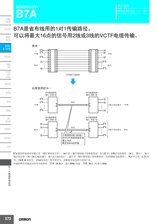
螺钉紧固端子
输入 (接收)
Ԏ᳡㋏㒳
模块
标准 (TYP. 19.2ms)
NPN对应输入 (不能连接2线性传
感器)
仅限- +-交互
标准 (TYP. 19.2ms)
TTL输入
--
型号 DRT1-B7AC
海外标准
U、 CU、 CE
型号
海外标准
B7A-T10S1 *1 B7A-T10S3 *1
U、C、 CE
B7A-T10M2
*2
--
型号
B7A-R6B11 B7A-R6B31 B7A-R6C11 B7A-R6C31 B7A-R6F11 B7A-R6F31 B7A-R6G11 B7A-R6G31 B7A-R6B16 B7A-R6B36 B7A-R6C16 B7A-R6C36 B7A-R6F16 B7A-R6F36 B7A-R6G16 B7A-R6G36 B7AS-R6B11
输出 32点
(16点×2端口)
输入
输入 64点 (16点×4端口)
输出
输出 64点 (16点×4端口)
传输延迟时间
错误时的输出处理 I/O单元占有CH
标准 (TYP. 19.2ms)
高速 (TYP. 3ms)
可切换
HOLD (仅限输入)
HOLD --
输入2CH 输出2CH
输入形态
+-端子结构
NPN对应输入
+-交互
输入形态 NPN对应输入 PNP对应输入 NPN对应输入 PNP对应输入
+-端子结构 仅限-
+-交互 +-交互
仅限- +-交互 +-交互
NPN对应输入
+-交互
TTL输入
--
NPN输入
733机型熟悉的讲义

飞机制造商为了加速飞机的生产,按设计和 工艺要求将飞机分成许多段件,生产后再 组装成整架飞机。
B737-300机身分成四段:41、43、46、 48
2020/12/21
Training Division of Maintenance and Engineering Dept.
12
B737飞机基本ion of Maintenance and Engineering Dept.
35
36章 气源系统
APU和地面气源也可以给系统提供气源。 APU给气源系统的左半部分提供气源,地 面气源给右半部分提供气源。
交输引气管附近上装了两个压力传感器, 分别指示左右部分的引气压力。
亿飞行小时,2.32亿个航班,759亿海里。 目前全球共有104个国家的347家航空公司拥有
737系列飞机。
2020/12/21
Training Division of Maintenance and Engineering Dept.
8
B737飞机基本介绍
➢ 基本尺寸
3.76m
28.88m
11.13m
2020/12/21
Training Division of Maintenance and Engineering Dept.
13
B737飞机基本介绍
➢ 飞机区域编号
2020/12/21
Training Division of Maintenance and Engineering Dept.
14
2020/12/21
Training Division of Maintenance and Engineering Dept.
10
RQA0008NXAQS中文资料

RQA0008NXAQSSilicon N-Channel MOS FETREJ03G1569-0100Rev.1.00Jul 04, 2007Features• High Output Power, High Gain, High EfficiencyPout = +36 dBm, Linear Gain = 18 dB, PAE = 65% (f = 520 MHz)• Compact package capable of surface mountingOutline*UPAK is a trademark of Renesas Technology Corp.Absolute Maximum Ratings(Ta = 25°C)UnitRatingsItem SymbolDrain to source voltage V DSS 16 V Gate to source voltage V GSS ±5 V Drain current I D 2.4 A Channel dissipation Pch note 10 W Channel temperature Tch 150 °CStorage temperature Tstg –55 to +150 °CNote: Value at Tc = 25°CThis device is sensitive to electro static discharge. An adequate careful handling procedure is requested.Electrical Characteristics(Ta = 25°C)Item Symbol Min. Typ Max. Unit Test ConditionsZero gate voltage drain current I DSS — — 10 µA V DS = 16 V, V GS = 0 Gate to source leak current I GSS — — ±2 µA V GS = ±5 V, V DS = 0 Gate to source cutoff voltage V GS(off) 0.15 0.4 0.8 V V DS = 6 V, I D = 1 mA Forward Transfer Admittance |yfs| — 2.4 — S V DS = 6 V, I D = 1.2 A Input capacitance Ciss — 44 — pF V GS = 5 V, V DS = 0, f = 1 MHz Output capacitance Coss — 25 — pF V DS = 6 V, V GS = 0, f = 1 MHz Reverse transfer capacitance Crss — 6.0 — pF V DG = 6 V, V GS = 0, f = 1 MHz — 36 — dBm Output Power Pout — 3.98 — WPower Added Efficiency PAE — 65 — % V DS = 6 V, I DQ = 400 mAf = 520 MHz, Pin = +20 dBmMain CharacteristicsEvaluation Circuit (f = 520 MHz)S Parameter(V DS = 6 V, I DQ = 400 mA, Zo = 50 Ω)S11 S21 S12 S22(deg.) MAG ANG(deg.)(deg.)MAG ANGf(MHz) MAG ANG(deg.) MAG ANG100 0.883 -170.0 8.48 84.9 0.021 -3.0 0.867 -175.4 150 0.904 -175.7 5.46 80.1 0.021 -5.3 0.879 -177.3 200 0.902 -178.2 4.13 72.6 0.021 -12.0 0.872 -178.5 250 0.900 179.6 3.30 67.1 0.021 -16.5 0.872 -179.7 300 0.898 177.8 2.75 61.6 0.021 -19.8 0.873 179.5 350 0.898 176.2 2.34 56.2 0.020 -24.2 0.873 178.8 400 0.897 174.8 2.04 50.9 0.020 -27.7 0.874 178.4 450 0.898 173.4 1.80 45.7 0.020 -31.3 0.873 177.8 500 0.899 172.3 1.61 40.7 0.020 -34.4 0.873 177.4 550 0.900 171.2 1.46 35.5 0.019 -38.2 0.875 176.8 600 0.900 170.1 1.33 30.5 0.019 -41.5 0.876 176.5 650 0.899 169.0 1.22 25.5 0.019 -45.0 0.876 176.0 700 0.899 167.9 1.13 20.5 0.019 -47.8 0.878 175.6 750 0.899 166.9 1.04 15.6 0.018 -51.2 0.878 175.2 800 0.898 165.8 0.97 10.6 0.018 -54.8 0.880 174.9 850 0.899 164.7 0.91 5.7 0.018 -57.4 0.878 174.4 900 0.901 163.7 0.85 0.9 0.018 -60.9 0.880 173.9 950 0.903 162.7 0.80 -3.9 0.017 -63.5 0.882 173.5 1000 0.903 161.8 0.75 -8.7 0.017 -66.5 0.883 173.1 1050 0.903 160.8 0.71 -13.4 0.017 -69.3 0.884 172.6 1100 0.905 159.8 0.68 -18.1 0.016 -71.9 0.883 172.1 1150 0.906 158.8 0.64 -22.8 0.016 -74.8 0.886 171.6 1200 0.907 157.8 0.61 -27.3 0.016 -76.8 0.888 171.2 1250 0.909 156.8 0.58 -32.0 0.015 -79.6 0.891 170.8 1300 0.911 155.8 0.55 -36.6 0.015 -81.9 0.893 170.4 1350 0.912 154.9 0.52 -41.2 0.015 -84.1 0.896 170.0 1400 0.912 154.0 0.50 -45.8 0.015 -86.2 0.897 169.5 1450 0.912 153.1 0.48 -50.3 0.014 -88.6 0.898 169.1 1500 0.913 152.1 0.46 -54.8 0.014 -90.2 0.900 168.7 1550 0.914 151.2 0.44 -59.2 0.014 -92.6 0.900 168.4 1600 0.915 150.3 0.42 -63.8 0.014 -94.1 0.902 167.8 1650 0.916 149.4 0.40 -68.3 0.013 -95.9 0.903 167.4 1700 0.915 148.5 0.39 -72.6 0.013 -97.6 0.904 167.0 1750 0.914 147.6 0.38 -76.9 0.013 -99.0 0.904 166.4 1800 0.913 146.7 0.36 -81.1 0.013 -100.8 0.906 165.8 1850 0.915 145.7 0.35 -85.3 0.013 -102.2 0.909 165.5 1900 0.920 144.5 0.34 -89.5 0.013 -103.9 0.909 165.0 1950 0.923 143.3 0.33 -93.6 0.013 -105.8 0.910 164.5 2000 0.925 142.3 0.31 -97.9 0.013 -107.2 0.911 163.9 2050 0.926 141.4 0.30 -102.1 0.013 -108.7 0.913 163.5 2100 0.928 140.5 0.29 -106.3 0.013 -109.9 0.914 163.0 2150 0.929 139.6 0.28 -110.6 0.013 -112.2 0.916 162.4 2200 0.930 138.7 0.27 -114.7 0.013 -112.8 0.917 161.8 2250 0.932 137.8 0.27 -118.9 0.013 -114.9 0.921 161.5 2300 0.931 137.1 0.26 -123.0 0.013 -116.5 0.921 161.0 2350 0.930 136.3 0.25 -127.1 0.013 -118.5 0.921 160.5 2400 0.926 135.5 0.24 -131.2 0.013 -120.2 0.924 159.9 2450 0.922 134.4 0.24 -135.4 0.014 -121.9 0.923 159.5 2500 0.920 133.3 0.23 -139.5 0.014 -123.7 0.921 159.0Package DimensionsOrdering InformationPart Name Quantity Shipping Containerφ178 mm reel, 12 mm emboss tapingRQA0008NXTL-E 1000pcs.Note: For some grades, production may be terminated. Please contact the Renesas sales office to check the state of production before ordering the product.Refer to "/en/network " for the latest and detailed information.Renesas Technology America, Inc.450 Holger Way, San Jose, CA 95134-1368, U.S.A Tel: <1> (408) 382-7500, Fax: <1> (408) 382-7501Renesas Technology Europe LimitedDukes Meadow, Millboard Road, Bourne End, Buckinghamshire, SL8 5FH, U.K.Tel: <44> (1628) 585-100, Fax: <44> (1628) 585-900Renesas Technology (Shanghai) Co., Ltd.Unit 204, 205, AZIACenter, No.1233 Lujiazui Ring Rd, Pudong District, Shanghai, China 200120Tel: <86> (21) 5877-1818, Fax: <86> (21) 6887-7898Renesas Technology Hong Kong Ltd.7th Floor, North Tower, World Finance Centre, Harbour City, 1 Canton Road, Tsimshatsui, Kowloon, Hong Kong Tel: <852> 2265-6688, Fax: <852> 2730-6071Renesas Technology Taiwan Co., Ltd.10th Floor, No.99, Fushing North Road, Taipei, Taiwan Tel: <886> (2) 2715-2888, Fax: <886> (2) 2713-2999Renesas Technology Singapore Pte. Ltd.1 Harbour Front Avenue, #06-10, Keppel Bay Tower, Singapore 098632 Tel: <65> 6213-0200, Fax: <65> 6278-8001Renesas Technology Korea Co., Ltd.Kukje Center Bldg. 18th Fl., 191, 2-ka, Hangang-ro, Yongsan-ku, Seoul 140-702, Korea Tel: <82> (2) 796-3115, Fax: <82> (2) 796-2145Renesas Technology Malaysia Sdn. BhdUnit 906, Block B, Menara Amcorp, Amcorp Trade Centre, No.18, Jalan Persiaran Barat, 46050 Petaling Jaya, Selangor Darul Ehsan, Malaysia Tel: <603> 7955-9390, Fax: <603> 7955-9510RENESAS SALES OFFICES。
AN7337NS资料

AN7337NS
7-element graphic equalizer IC for Hi-Fi audio equipment
s Overview
The AN7337NS is a graphic equalizer IC for high performance Hi-Fi audio equipment developed for deck. It incorporates an output buffer circuit and 7 resonance buffer circuits, and can set resonance frequency by external capacitor.
GND
17
or m
SOP020-P-0300B
at io n.
1
AN7337NS
s Pin Descriptions
Pin No. 1 2 3 4 5 6 7 8 9 In 1 NF 1 In 2 NF 2 In 3 NF 3 In 4 In 5 NF 4 Description Pin No. 11 12 13 14 15 16 17 18 19 20
(1) If any of the products or technical information described in this book is to be exported or provided to non-residents, the laws and regulations of the exporting country, especially, those with regard to security export control, must be observed. (2) The technical information described in this book is intended only to show the main characteristics and application circuit examples of the products, and no license is granted under any intellectual property right or other right owned by our company or any other company. Therefore, no responsibility is assumed by our company as to the infringement upon any such right owned by any other company which may arise as a result of the use of technical information described in this book. (3) The products described in this book are intended to be used for standard applications or general electronic equipment (such as office equipment, communications equipment, measuring instruments and household appliances). Consult our sales staff in advance for information on the following applications: – Special applications (such as for airplanes, aerospace, automobiles, traffic control equipment, combustion equipment, life support systems and safety devices) in which exceptional quality and reliability are required, or if the failure or malfunction of the products may directly jeopardize life or harm the human body. – Any applications other than the standard applications intended. (4) The products and product specifications described in this book are subject to change without notice for modification and/or improvement. At the final stage of your design, purchasing, or use of the products, therefore, ask for the most up-to-date Product Standards in advance to make sure that the latest specifications satisfy your requirements. (5) When designing your equipment, comply with the range of absolute maximum rating and the guaranteed operating conditions (operating power supply voltage and operating environment etc.). Especially, please be careful not to exceed the range of absolute maximum rating on the transient state, such as power-on, power-off and mode-switching. Otherwise, we will not be liable for any defect which may arise later in your equipment. Even when the products are used within the guaranteed values, take into the consideration of incidence of break down and failure mode, possible to occur to semiconductor products. Measures on the systems such as redundant design, arresting the spread of fire or preventing glitch are recommended in order to prevent physical injury, fire, social damages, for example, by using the products. (6) Comply with the instructions for use in order to prevent breakdown and characteristics change due to external factors (ESD, EOS, thermal stress and mechanical stress) at the time of handling, mounting or at customer's process. When using products for which damp-proof packing is required, satisfy the conditions, such as shelf life and the elapsed time since first opening the packages. (7) This book may be not reprinted or reproduced whether wholly or partially, without the prior written permission of Matsushita Electric Industrial Co., Ltd.
AN7333S中文资料
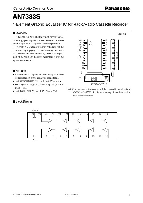
I Block Diagram
GND 24 23
22
21
20
19
18
17
16
15
14
1 VCC
2
3
45678 Nhomakorabea9
10
11
0.15 0.925
13
12
2.0±0.2
I Features
15.3±0.3
1.27
Publication date: December 2001
SDC00022BEB
1
元器件交易网
AN7333S
1 VCC
2
3
4
5
6 0.056 µF 0.68 µF
7
8 0.018 µF 0.22 µF
50 kΩ VR
9
10
11
12 0.0018 µF 0.022 µF
50 kΩ VR
0.0056 µF 0.068 µF
50 kΩ VR
50 kΩ VR
50 kΩ VR
10 µF 4.7 kΩ 10 µF 0.0047 µF 10 kΩ
Rating 14.4 30 432 −20 to +75 −55 to +125
N系列射频同轴连接器

1.5
20
2.0
36
1.5
20
2.0
17
2.0
h×t 0.3×2.0 0.3×2.0 0.5×2.0 0.2×2.5 0.2×2.2
A×A 19.0×19.0 17.5×17.5 19.0×19.0 17.5×17.5 17.0×17.0
B 14.0 12.7 14.0 12.7 13.0
5
型
号
N-KFD137
Ф 5.3
SFF-50-3-1
SYV-50-3
号
D
A
B
配接电缆型号
Ф 4.3 5.0 10.0 SFF-50-2-2
SYV-50-2-2
Ф 5.3 5.0 10.0 SFF-50-3-1
SYV-50-3
Ф 10.3 5.5 11.5
SYV-50-7-1
Ф 11.5 7.7 15.0
SYV-50-7-2
L
L1
29.6
4.1
28.3
5.5
25.0
5.0
26.0
4.0
L2
d2
D
d1×h
2.8
Ф 7.7
Ф 7.9
Ф 1.0×0.35
2.8
Ф 7.7
Ф 7.9
Ф 1.0×0.35
2.0
Ф 6.0
Ф 6.2
Ф 1.3×0.25
2.0
Ф 6.0
Ф 6.2
Ф 1.0×0.2
L
L1
L2
L3
25.7
8
5
2
L
L1
18
Ф 4.1
Ф 4.2
型
号
L
AO4707中文资料

Symbol Units R θJL R θJL40°C/WMaximum Junction-to-Ambient A Steady-State 6775Maximum Junction-to-Lead CSteady-State2530Maximum Junction-to-AmbientA t ≤ 10s R θJA 36°C/W5421Thermal Characteristics Schottky Maximum Junction-to-Ambient A t ≤ 10s R θJA 2475Maximum Junction-to-Lead CParameter: Thermal Characteristics MOSFETTyp Max Steady-State 3040Maximum Junction-to-Ambient ASteady-State AO4707AO4707SymbolMin TypMaxUnits BV DSS -30V -1T J =55°C-5I GSS ±100nA V GS(th)-1.2-2-2.4V I D(ON)40A 24.533T J =125°C334156m Ωg FS 14.5S V SD -0.76-1V I S-4.2A C iss 920pF C oss 190pF C rss 122pF R g3.6ΩQ g (10V)18.4nC Q g (4.5V)9.3nC Q gs 2.7nC Q gd 4.9nC t D(on)7.1ns t r 3.4ns t D(off)18.9ns t f 8.4ns t rr 21.5ns Q rr12.5nC SCHOTTKY PARAMETERS V F 0.480.52V0.070.154.2201560C T120pF THIS PRODUCT HAS BEEN DESIGNED AND QUALIFIED FOR THE CONSUMER MARKET. APPLICATIONS OR USES AS CRITICAL COMPONENTS IN LIFE SUPPORT DEVICES OR SYSTEMS ARE NOT AUTHORIZED. AOS DOES NOT ASSUME ANY LIABILITY ARISING OUT OF SUCH APPLICATIONS OR USES OF ITS PRODUCTS. AOS RESERVES THE RIGHT TO IMPROVE PRODUCT DESIGN,FUNCTIONS AND RELIABILITY WITHOUT NOTICEMaximum Body-Diode Continuous CurrentInput Capacitance Output Capacitance Turn-On DelayTime DYNAMIC PARAMETERS V GS =0V, V DS =-15V, f=1MHz Gate Drain Charge Total Gate Charge (10V)V GS =-10V, V DS =-15V, I D =-8ATurn-On Rise Time Turn-Off DelayTime V GS =-10V, V DS =-15V, R L =1.8Ω, R GEN =3ΩGate resistanceV GS =0V, V DS =0V, f=1MHzTurn-Off Fall TimeSWITCHING PARAMETERSTotal Gate Charge (4.5V)Gate Source Charge m ΩV GS =-4.5V, I D =-5AI S =-1A,V GS =0VV DS =-5V, I D =-8AR DS(ON)Static Drain-Source On-ResistanceForward TransconductanceDiode Forward Voltage I DSS µA Gate Threshold Voltage V DS =V GS I D =-250µA V DS =-24V, V GS =0VV DS =0V, V GS =±20V Zero Gate Voltage Drain Current Gate-Body leakage current Electrical Characteristics (T J =25°C unless otherwise noted)STATIC PARAMETERS Parameter Conditions Body Diode Reverse Recovery TimeBody Diode Reverse Recovery Charge I F =-8A, dI/dt=100A/µsDrain-Source Breakdown Voltage On state drain currentI D =-250µA, V GS =0V V GS =-10V, V DS =-5V V GS =-10V, I D =-8AReverse Transfer Capacitance I F =-8A, dI/dt=100A/µsForward Voltage Drop I F =3.0AI rm Maximum reverse leakage current V R =24VmAV R =24V, T J =125°C V R =24V, T J =150°C Junction CapacitanceV R =15VA: The value of R θJA is measured with the device mounted on 1in 2 FR-4 board with 2oz. Copper, in a still air environment with T A =25°C. The value in any given application depends on the user's specific board design. The current rating is based on the t ≤ 10s thermal resistance rating.B: Repetitive rating, pulse width limited by junction temperature.C. The R θJA is the sum of the thermal impedence from junction to lead R θJL and lead to ambient.D. The static characteristics in Figures 1 to 6,12,14 are obtained using 80 µs pulses, duty cycle 0.5% max.E. These tests are performed with the device mounted on 1 in 2 FR-4 board with 2oz. Copper, in a still air environment with T A =25°C. The SOA curve provides a single pulse rating. Rev4: August 2005AO4707AO4707AO4707。
- 1、下载文档前请自行甄别文档内容的完整性,平台不提供额外的编辑、内容补充、找答案等附加服务。
- 2、"仅部分预览"的文档,不可在线预览部分如存在完整性等问题,可反馈申请退款(可完整预览的文档不适用该条件!)。
- 3、如文档侵犯您的权益,请联系客服反馈,我们会尽快为您处理(人工客服工作时间:9:00-18:30)。
TC
−20 to +60ห้องสมุดไป่ตู้
°C
Storage Temperature
Tstg
−40 to +85
°C
Lead Soldering Temperature
Tsld
260 (10 sec)
°C
Relative Humidity (noncondensing) RH
85
%
*1 Pulse Condition: Pulse Width (PW) = 10 µs, Duty = 1%
Optical Fiber
SMF Length = 1 m
φ 0.9 φ7
2 4 27.4
2– φ 2.2
φ6 12.7 17.0
PIN CONNECTIONS
P.C.D. = φ 2 4 3 1 2
1 3.7
7.2
20
φ 0.45
1
2
LD
CASE
The information in this document is subject to change without notice. Before using this document, please confirm that this is the latest version.
Restricted Substance per RoHS
Lead (Pb) Mercury Cadmium Hexavalent Chromium PBB PBDE
Concentration Limit per RoHS (values are not yet fixed) < 1000 PPM < 1000 PPM < 100 PPM < 1000 PPM < 1000 PPM < 1000 PPM
nm
Minimum Fiber Bending Radius
30
mm
Fiber Length
1 000 MIN.
mm
Fiber Length: 1 000 mm MIN.
NX7337BF-AA
Ferrule
2
Data Sheet GBB-SA-1692
元器件交易网
NX7337BF-AA
ABSOLUTE MAXIMUM RATINGS (TC = 25°C, unless otherwise specified)
Parameter
Symbol
Ratings
Unit
Pulsed Forward Current*1
IFP
1.2
A
Reverse Voltage
VR
2.0
V
Operating Case Temperature
FEATURES
• High output power • Long wavelength
Pf = 180 mW @ IFP = 1 000 mA*1 λC = 1 310 nm
*1 Pulse Conditions: Pulse width (PW) = 10 µs, Duty = 1%
PACKAGE DIMENSIONS (UNIT: mm)
MIN. TYP. MAX. Unit
80
mA
75
mW
1 280
1 342.5 nm
0.35
nm/° C
10
nm
Data Sheet GBB-SA-1692
3
元器件交易网
REFERENCE
Document Name Optical semiconducrtor devices for fiberoptic communications Selection Guide Opto-Electronics Devices Pamphlet Opto-Electronics Devices (CD-ROM) NEC semiconductor device reliability/quality control system*1 Quality grades on NEC semiconductor devices*1 SEMICONDUCTOR SELECTION GUIDE −Products and Packages−*1
Important Information and Disclaimer: Information provided by CEL on its website or in other communications concerting the substance content of its products represents knowledge and belief as of the date that it is provided. CEL bases its knowledge and belief on information provided by third parties and makes no representation or warranty as to the accuracy of such information. Efforts are underway to better integrate information from third parties. CEL has taken and continues to take reasonable steps to provide representative and accurate information but may not have conducted destructive testing or chemical analysis on incoming materials and chemicals. CEL and CEL suppliers consider certain information to be proprietary, and thus CAS numbers and other limited information may not be available for release. In no event shall CEL’s liability arising out of such information exceed the total purchase price of the CEL part(s) at issue sold by CEL to customer on an annual basis. See CEL Terms and Conditions for additional clarification of warranties and liability.
I th
Pf
IFP = 1000 mA,
PW = 10 µs, Duty = 1%
λC RMS (−20 dB), IFP = 1 000 mA, PW = 10 µs, Duty = 1 %
∆λ /∆T
σ
RMS (−20 dB), IFP = 1 000 mA,
PW = 10 µs, Duty = 1 %
9.3±0.5
µm
Cladding Diameter
125±2
µm
Maximum Cladding Noncircularity
2
%
Maximum Core/Cladding Concentricity
1.6
%
Outer Diameter
0.9±0.1
mm
Cut-off Wavelength
1 140 to 1 280
σ
RMS (−20 dB), IFP = 1 000 mA,
PW = 10 µs, Duty = 1%
tr
10-90%
tf
90-10%
MIN. TYP. MAX. Unit
2.5
4.0
V
35
65
mA
110
180
mW
1 290 1 310 1 330
nm
4.5
10.0
nm
2.0
ns
2.0
ns
ELECTRO-OPTICAL CHARACTERISTICS (TC = 0 to +60°C)
Subject: Compliance with EU Directives
CEL certifies, to its knowledge, that semiconductor and laser products detailed below are compliant with the requirements of European Union (EU) Directive 2002/95/EC Restriction on Use of Hazardous Substances in electrical and electronic equipment (RoHS) and the requirements of EU Directive 2003/11/EC Restriction on Penta and Octa BDE. CEL Pb-free products have the same base part number with a suffix added. The suffix –A indicates that the device is Pb-free. The –AZ suffix is used to designate devices containing Pb which are exempted from the requirement of RoHS directive (*). In all cases the devices have Pb-free terminals. All devices with these suffixes meet the requirements of the RoHS directive. This status is based on CEL’s understanding of the EU Directives and knowledge of the materials that go into its products as of the date of disclosure of this information.