5550LN103K4中文资料
硒鼓型号对照表
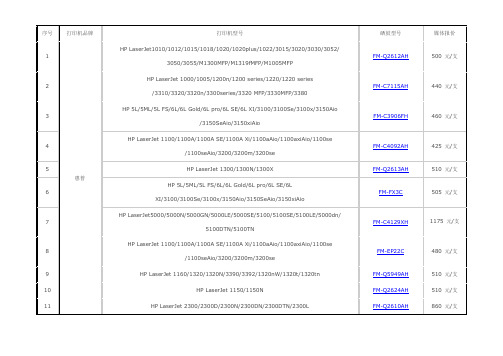
1090元/支
20
HP LaserJet 5200/5200L/5200LN/5200dtn/5200n/5200tn/5200Lx
FM-Q7516AH
1150元/支
21
HP LaserJet P2015d/2010/2014/2014n/M2727nfMFP/M2727nfsMFP
FM-C3906FH
460元/支
4
HP LaserJet 1100/1100A/1100ASE/1100AXi/1100aAio/1100axiAio/1100se
/1100seAio/3200/3200m/3200se
FM-C4092AH
425元/支
5
HP LaserJet 1300/1300N/1300X
FM-C972Color LaserJet 4600/4600n/4600dn/4600dtn/4600hdn/4650dn/4650dtn/4650hdn
FM-C9723AH
1505元/支
32
HP Color LaserJet 1500/1500L/2500/2500L/2500n/2500tn/2550/2550L/2550n/
5100DTN/5100TN
FM-C4129XH
1175元/支
8
HP LaserJet 1100/1100A/1100ASE/1100AXi/1100aAio/1100axiAio/1100se
/1100seAio/3200/3200m/3200se
FM-EP22C
480元/支
9
HP LaserJet 1160/1320/1320N/3390/3392/1320nW/1320t/1320tn
双通道低成本模数转换器cs5550中文
4 寄存器描述…………………………………………………………………………..…………………..18 4.1 配置寄存器………………………………………………………………………………...18 4.2 DC偏移寄存器…………………………………………………………………………...19 4.3 AC/DC增益寄存器……………………………………………………………………..19 4.4 周期计数寄存器…………………………………………………………………………...19 4.5 输出寄存器………………………………………………………………………………...20 4.6 滤波输出寄存器…………………………………………………………………………...20 4.7 状态寄存器和屏蔽寄存器………………………………………………………………...20 4.8 AC偏移寄存器…………………………………………………………………………...21 4.9 温度传感器数据输出寄存器………………………...……………………………………21 4.10 控制寄存器………………………………………………………………………………...21
4 of 22
8/11/03
1. 特性与规格说明 . 最大值和最小值参数是指在所有的操作条件可被保证的值.
. 典型参数是在标准供电和25°C时的测量值. . DGND = 0V.所有电压是指对 0V 的电压值.
模拟特性
参数
符号 最小值
精度(两个通道)
共模抑制比
CMRR
80
偏移漂移
-
模拟输入(AIN1±) 差分输入范围 {(AIN1+) - (AIN1- )}
测量和参考输入
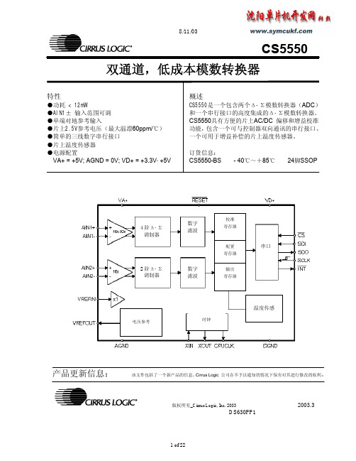
差分模拟输入9,10,15,16 AIN1+, AIN1-, AIN2+, AIN2- —差分模拟输入引脚。
LNSK10中文资料

FEATURESMultilayer structure allows diverse resistance value in the same B constantMultilayer structure allows lower resistance at high B constant.Solder plating with Ni barrier gives high reliability for both flow and reflow soldering.Unified shape and tightly controlled dimension is fit to high mounting speed.APPLICATIONSTemperature compensation for crystal oscillator (TCXO)Temperature compensation for Personal computer Temperature detection for CPU and memory device Temperature detection for battery packTemperature compensation for contrast of LCDLNS V 16 G 103 J PDESCRIPTIONThe LNS series is manganese oxide based NTC thermistor,which shows non-linear resistance-temperature behavior.Multilayered structure has as high reliability as monoblock type,even without protective glass coating, since the active electrode and sensor layer is buried inside the ceramic body.NTC Thermistor SMDSeries B constantZ 3250K K 3435K Y 3670K W 3890K A 3970K V 4150K U 4550K T 4750KChip size (mm)10 1.0 x 0.5 x 0.5 (inches 0402)16 1.6 x 0.8 x 0.8 (inches 0603)202.0 x 1.2 x 0.8 (inches 0805)Resistance at 25 ¡10110 ¡¿101= 100¥10210 ¡¿102= 1 K ¥10310 ¡¿103= 10 K ¥PackageP Paper taping E Emboss taping BBulkResistance deviation rangeF ¡1£¥H ¡3£¥J ¡5£¥K¡10£¥ORDERING INFORMATIONB constant deviation rangeF ¡1%G ¡2%H¡3%SPECIFICATIONS1005(0402) sizeResistance @ 25o CThe zero-power resistance at the standard temperature of 25o C. The zero-power resistance means the value of DC resistance of a thermistor measured at a specified temperature, with electric load being kept so small that there is no noticeable change in the measured resistance by the influence of the applied electric load.Bconstant 25 / 85B = ln(R0/R1) / (1/T- 1/T1) Without special note, B constant is calculated from the resistance values at 25o C and 85o C[B25/85], which is the most common.Dissipation constant (¥‰)Dissipation factor is defined as the ratio at a specified ambient temperature of a change in power dissipation in a thermistor to the resultant body temperature change.¡⁄¥= P/( T1- 25o C) mW/ o C¡⁄P : dissipated power¡⁄T1 : thermistor temp, 85¡0.1o CMaximum power rating PThis is the maximum handling power, keeping its temperature not exceeding the allowed maximum temperature for operation.¡⁄P max = ¥(T max- T a)¡⁄¥:dissipation constant¡⁄T a:25o C¡⁄T max:125o CThermal Time ConstantThe time necessary for an unloaded thermistor to vary its temperature by 63.2%of the difference between its initial and final temperatures. Initial temperature is 85¡0.1o C and final1608(0603) sizeResistance @ 25o CThe zero-power resistance at the standard temperature of 25o C. The zero-power resistance means the value of DC resistance of a thermistor measured at a specified temperature, with electric load being kept so small that there is no noticeable change in the measured resistance by the influence of the applied electric load.Bconstant 25 / 85B = ln(R0/R1) / (1/T- 1/T1) Without special note, B constant is calculated from the resistance values at 25o C and 85o C[B25/85], which is the most common.Dissipation constant (¥‰)Dissipation factor is defined as the ratio at a specified ambient temperature of a change in power dissipation in a thermistor to the resultant body temperature change.¡⁄¥= P/( T1- 25o C) mW/ o C¡⁄P : dissipated power¡⁄T1 : thermistor temp, 85¡0.1o CMaximum power rating PThis is the maximum handling power, keeping its temperature not exceeding the allowed maximum temperature for operation.¡⁄P max = ¥(T max- T a)¡⁄¥:dissipation constant¡⁄T a:25o C¡⁄T max:125o CThermal Time ConstantThe time necessary for an unloaded thermistor to vary its temperature by 63.2%of the difference between its initial and final temperatures. Initial temperature is 85¡0.1o C and final temperature is 47.1¡0.1o C.Resistance @ 25o CThe zero-power resistance at the standard temperature of 25o C . The zero-power resistance means the value of DC resistance of a thermistor measured at a specified temperature,with electric load being kept so small that there is no noticeable change in the measured resistance by the influence of the applied electric load.Bconstant 25 / 85B = ln(R 0/R 1) / (1/T 0- 1/T 1) Without special note, B constant is calculated from the resistance values at 25oC and 85o C [B25/85], which is the most common.Dissipation constant (¥‰)Dissipation factor is defined as the ratio at a specified ambient temperature of a change in power dissipation in a thermistor to the resultant body temperature change. ¡⁄¥= P/( T 1- 25o C ) mW/ o C ¡⁄P : dissipated power ¡⁄T1 : thermistor temp, 85¡0.1o C Maximum power rating PThis is the maximum handling power, keeping its temperature not exceeding the allowed maximum temperature for operation. ¡⁄P max = ¥(T max - T a )¡⁄¥:dissipation constant ¡⁄T a :25o C ¡⁄T max :125o C Thermal Time ConstantThe time necessary for an unloaded thermistor to vary its temperature by 63.2%of the difference between its initial and final temperatures. Initial temperature is 85¡0.1o C and final temperature is 47.1¡0.1o C .2012(0805) sizeRESISTANCE VS. TEMPERATURE TABLERELIABILITY TEST METHODStructure and Dimension CHIP STRUCTURECHIP DIMENSIONSize A B C D E F G H Jtnote 1608 1.0¡0.1 1.9¡0.18.0¡0.1 3.5¡0.05 1.75¡0.1 4.0¡0.1 2.0¡0.05 4.0¡0.1 1.5+0.1-0.00.23¡0.02paper 10050.62¡0.04 1.12¡0.048.0¡0.1 3.5¡0.05 1.75¡0.1 4.0¡0.1 2.0¡0.05 4.0¡0.1 1.5+0.1-0.00.6¡0.05paperTape and Reel Packaging for Paper PackageStructure of TapingTaping must have leader and empty component compartment as shown in the following figure.Size A B W F E P1P2P0D0t1t2note 3216 1.73¡0.1 3.56¡0.18.0+0.3-0.1 3.5¡0.05 1.75¡0.1 4.0¡0.1 2.0¡0.05 4.0¡0.1 1.5+0.1-0.00.23¡0.02 1.14¡0.1emboss 2012 1.45¡0.1 2.25¡0.18.0+0.3-0.1 3.5¡0.05 1.75¡0.1 4.0¡0.1 2.0¡0.05 4.0¡0.1 1.5+0.1-0.00.23¡0.02 1.0¡0.1embossTape and Reel Packaging for Emboss PackagePackage Quantity12,000(pcs/Reel) - 1005 size4,000(pcs/Reel) - 1608, 2012, 3216 sizePackagingRecommended Land PatternSolderingHand soldering : 280o C max., 5sec max.Reflow profileComponent LayoutLocate the product horizontal to the direction at which bending is applied.Component MountingSMT Process CharacteristicsSolder and FluxSolder : Eutetic solder recommended Flux : Rosin based flux recommendedHalogen content 0.2 w% or less recommendedFlow profile。
京瓷零件手册TASKalfa 3050ci 3550ci 4550ci 5550ci零件手册

Part.No.
302LC04031 302LC04051 302LC04063 302LC04071 302LC04191 302LC04200 302LC04212 302LC04250 302LC04260 302LC04280 302LC04290 302LC04410 302LC04720 302LC04651 302LC34050 302LC04271 302LC34010 302LM34010 302LN34010 302LK34010 2FB04270 302FZ04950 302LC04011 302LC94520 302LC04460 302LC04490 302LC04500 302H094300 302LC02710 302LC02720 302LC02730 302LC02760 302LC04240 302LC46230 302LC04730 302LC04751 302LW04260 302LC04740
-1-
FIG. 1 Covers 1
2LK/2LN/2LM/2LC-3
6
101
13
1
101ALeabharlann 5 71013
8
104
35 22 22 34 33 23 18 24
104 104 104 104 102 A 105 104 104 102 101
104
12 11
34 14 32
22
22
15 28 30 27 25 26
Description
COVER TOP TRAY COVER RIGHT LOWER F COVER RIGHT MIDDLE R COVER RIGHT LOWER R COVER EXIT COVER TRAY REAR COVER ISU BOTTOM COVER INNER LEFT COVER INNER FEED F COVER HANDLE COVER MAIN SWITCH MOUNT FRONT COVER LEFT STOPPER ORIGINAL STRAP FRONT COVER LABEL SW CAUTION EN EMBLEM SHEET EMBLEM 5550C SHEET EMBLEM 4550C SHEET EMBLEM 3550C SHEET EMBLEM 3050C PLATE MAGNET SPONGE TRAY WASTE COVER FRONT A PARTS COVER FRONT SP STOPPER CONTAINER PLATE FRONT COVER SPONGE COVER FRONT PARTS,HUMIDITY SENSOR,SP COVER HUMIDITY SENSOR SHEET HUMIDITY SENSOR A SHEET HUMIDITY SENSOR B SHEET COVER HUMIDITY SENSOR COVER FRONT RIGHT LOWER WIRE FRONT LOW SHEET COVER FRONT SPONGE COVER FRONT B SPACER USB SHEET COVER FRONT B
研工(KinSoon)55寸户外高亮液晶显示屏KSN550SN01-A03规格书
Gate Driver Circuit
TFT - LCD Panel
(1920 × RGB × 1080 pixels)
G1080
+12.0V
Power Circuit Block
Power Signals
V : 10Block +24.0V, GND, On/off Ext VBR-B
LED Driver
2000 cd/m2 (Center 1point ,Typ.)
Viewing angle free ( R/L 178 (Min.), U/D 178 (Min.)) Total 241W (Typ.) [Logic=12.9W, Backlight=228.1W(@EXTVBR-B = 100%) 18,100 g (Typ.) Transmissive mode, Normally black Hard coating(3H), Anti-reflection treatment of the front polarizer (Reflectance〈 2%) Landscape and Portrait Enabled
E53NA50中文资料

E53NA50中文资料STE53NA50N -CHANNEL ENHANCEMENT MODEFAST POWER MOS TRANSISTORs TYPICAL R DS(on)=0.075?s HIGH CURRENT POWER MODULE s AVALANCHE RUGGED TECHNOLOGYsVERY LARGE SOA -LARGE PEAK POWER CAPABILITYs EASY TO MOUNTsSAME CURRENT CAPABILITY FOR THE TWO SOURCE TERMINALSs EXTREMELY LOW Rth (Junction to case)sVERY LOW INTERNAL PARASITIC INDUCTANCEsISOLATED PACKAGE UL RECOGNIZEDAPPLICATIONS s SMPS &UPS s MOTOR CONTROL s WELDING EQUIPMENT s OUTPUT STAGE FOR PWM,ULTRASONIC CIRCUITSINTERNAL SCHEMATIC DIAGRAMFebruary 1998ABSOLUTE MAXIMUM RATINGSSymbol ParameterValue Unit V DS Drain-source Voltage (V GS =0)500V V DGR Drain-gate Voltage (R GS =20k ?)500V V GS Gate-source Voltage ±30V I D Drain Current (continuous)at T c =25oC 53A ID Drain Current (continuous)at T c =100o C 33A I DM(?)Drain Current (pulsed)212A P to t Total Dissipation at T c =25oC 460W Derating Factor 3.68W/o CT st g Storage Temperature-55to 150o C T j Max.Operating Junction Temperature 150oCV ISOInsulation Withhstand Voltage (AC-RMS)2500V (?)Pulse width limited by safe operating areaTYPE V DSS R DS(on)I D STE53NA50500V<0.085?53AISOTOP1/7THERMAL DATAR t hj-ca se R thc-h Thermal Resistance Junction-case Max Thermal Resistance Case-heatsink With ConductiveGrease Applied Max0.270.05o C/Wo C/WAVALANCHE CHARACTERISTICSSymbol Parameter Max Value UnitI AR Avalanche Current,Repetitive or Not-Repetitive(pulse width limited by T j max,δ <1%)26AE AS Single Pulse Avalanche Energy(starting T j=25o C,I D=I AR,V DD=50V)1014mJELECTRICAL CHARACTERISTICS(T case=25o C unless otherwise specified)OFFSymbol Parameter Test Conditions Min.Typ.Max.Unit V(BR)DSS Drain-sourceBreakdown VoltageI D=1mA V GS=0500VI DSS Zero Gate VoltageDrain Current(V GS=0)V DS=Max RatingV DS=Max Rating T c=125o C1001000μAμAI GSS Gate-body LeakageCurrent(V DS=0)V GS=±30V±400nA ON(?)Symbol Parameter Test Conditions Min.Typ.Max.Unit V GS(th)Gate ThresholdVoltageV DS=V GS I D=1mA 2.253 3.75VR DS(on)Static Drain-source OnResistanceV GS=10V I D=27A0.0750.085?I D(o n)On State Drain Current V DS>I D(on)x R DS(on)maxV GS=10V53A DYNAMICSymbol Parameter Test Conditions Min.Typ.Max.Unit g fs(?)ForwardTransconductanceV DS>I D(on)X RDS(on)MAX I D=27A25SC iss C oss C rss Input CapacitanceOutput CapacitanceReverse TransferCapacitanceV DS=25V f=1MHz V GS=0131500450162000650nFpFpFSTE53NA50 2/7ELECTRICAL CHARACTERISTICS(continued) SWITCHING ONSymbol Parameter Test Conditions Min.Typ.Max.Unit t d(on) t r Turn-on TimeRise TimeV DD=250V I D=27AR G=4.7 ?V GS=10V(see test circuit,figure1)579280130nsnsQ g Q gs Q gd Total Gate ChargeGate-Source ChargeGate-Drain ChargeV DD=400V I D=53A V GS=10V47054219658nCnCnCSWITCHING OFFSymbol Parameter Test Conditions Min.Typ.Max.Unit t r(Vof f) t ft c Off-voltage Rise TimeFall TimeCross-over TimeV DD=400V I D=53AR G=4.7 ?V GS=10V(see test circuit,figure3)1053614514550205nsnsnsSOURCE DRAIN DIODESymbol Parameter Test Conditions Min.Typ.Max.Unit I SD I SDM(?)Source-drain CurrentSource-drain Current(pulsed)53212AAV SD(?)Forward On Voltage I SD=53A V GS=0 1.6V t rr Q rr I RRM Reverse RecoveryTimeReverse RecoveryChargeReverse RecoveryCurrentI SD=53A di/dt=100A/μsV R=100V T j=150o C(see test circuit,figure3)100031.563nsμCA(?)Pulsed:Pulse duration=300μs,duty cycle1.5% (?)Pulse width limited by safe operating areaSafe Operating Area for Thermal ImpedanceSTE53NA503/7Output Characteristics TransconductanceGate Charge vs Gate-source Voltage Transfer Characteristics Static Drain-source On Resistance Capacitance VariationsSTE53NA50 4/7Normalized Gate Threshold Voltage vs TemperatureSource-drain Diode Forward Characteristics Fig.2:Gate Charge test Circuit Normalized On Resistance vs Temperature Fig.1:Switching Times Test Circuits For Resistive Load Fig.3:Test Circuit For Inductive Load Switching And Diode Recovery TimesSTE53NA505/7DIM.mm inch MIN.TYP.MAX.MIN.TYP.MAX.A 11.812.20.4660.480B 8.99.10.3500.358C 1.95 2.050.0760.080D 0.750.850.0290.033E 12.612.80.4960.503F 25.1525.50.990 1.003G 31.531.71.240 1.248H 40.157J 4.1 4.30.1610.169K 14.915.10.5860.594L 30.130.31.185 1.193M 37.838.21.488 1.503N 40.157O7.88.20.3070.322BEHONJ K L MFACGDISOTOP MECHANICAL DATASTE53NA506/7Information furnished is believed to be accurate and reliable.However,SGS-THOMSON Microelectronics assumes no responsability for the consequences of use of such information nor for any infringement of patents or other rights of third parties which may results from its use.No license is granted by implication or otherwise under any patent or patent rights of SGS-THOMSON Microelectronics.Specifications mentioned in this publication are subject to change without notice.This publication supersedes and replaces all information previously supplied.SGS-THOMSON Microelectronics products are not authorized for use as critical components in life support devices or systems without express written approval of SGS-THOMSON Microelectonics.1998SGS-THOMSON Microelectronics -Printed in Italy -All Rights ReservedSGS-THOMSON Microelectronics GROUP OF COMPANIESAustralia -Brazil -Canada -China -France -Germany -Italy -Japan -Korea -Malaysia -Malta -Morocco -The Netherlands -Singapore -Spain -Sweden -Switzerland -Taiwan -Thailand -United Kingdom -U.S.A...STE53NA50 7/7。
常用三极管参数大全

玉林万顺达电脑芯片级维修资料 2010-07-20整理玉林万顺达电脑芯片级维修资料 2010-07-20整理玉林万顺达电脑芯片级维修资料 2010-07-20整理玉林万顺达电脑芯片级维修资料 2010-07-20整理玉林万顺达电脑芯片级维修资料 2010-07-20整理玉林万顺达电脑芯片级维修资料 2010-07-20整理玉林万顺达电脑芯片级维修资料 2010-07-20整理玉林万顺达电脑芯片级维修资料 2010-07-20整理玉林万顺达电脑芯片级维修资料 2010-07-20整理玉林万顺达电脑芯片级维修资料 2010-07-20整理玉林万顺达电脑芯片级维修资料 2010-07-20整理玉林万顺达电脑芯片级维修资料 2010-07-20整理玉林万顺达电脑芯片级维修资料 2010-07-20整理玉林万顺达电脑芯片级维修资料 2010-07-20整理玉林万顺达电脑芯片级维修资料 2010-07-20整理玉林万顺达电脑芯片级维修资料 2010-07-20整理玉林万顺达电脑芯片级维修资料 2010-07-20整理玉林万顺达电脑芯片级维修资料 2010-07-20整理玉林万顺达电脑芯片级维修资料 2010-07-20整理玉林万顺达电脑芯片级维修资料 2010-07-20整理玉林万顺达电脑芯片级维修资料 2010-07-20整理玉林万顺达电脑芯片级维修资料 2010-07-20整理玉林万顺达电脑芯片级维修资料 2010-07-20整理玉林万顺达电脑芯片级维修资料 2010-07-20整理玉林万顺达电脑芯片级维修资料 2010-07-20整理玉林万顺达电脑芯片级维修资料 2010-07-20整理玉林万顺达电脑芯片级维修资料 2010-07-20整理玉林万顺达电脑芯片级维修资料 2010-07-20整理玉林万顺达电脑芯片级维修资料 2010-07-20整理玉林万顺达电脑芯片级维修资料 2010-07-20整理。
EPM240T100I5N中文资料(Altera)中文数据手册「EasyDatasheet - 矽搜」

256-Pin FineLine
BGA
324-Pin FineLine
BGA
0.5
0.5
1
1
49
121
289
361
7×7
11 × 11 17 × 17 19 × 19
芯片中文手册,看全文,戳
MAX II器件具有内部线性稳压器,它支持3.3 V或2.5 V外接电源电压,调节 供给下降到1.8 V MAX IIG和MAX IIZ器件内部工作电压只接受1.8 V外部电源. MAX IIZ器件引脚兼容100针微型FineLine BGA和256引脚微型FineLine BGA封装 MAX IIG设备.除外部电源电压要求,MAX II和MAX II G设备具有相同引脚 输出和时序规范.
f
有关等效宏单元详细信息,请参阅
宏单元转换方法
白皮书.
MAX II逻辑元素
MAX II和MAX IIG器件有三种速度等级:-3,-4,-5,与
-3是最快.同样,MAX IIZ器件有三种速度等级可供选择:-6,
-7,和-8,以-6是最快.这些速度等级代表总体相对
性能,而不是任何特定时序参数.对于传播延迟定时
由MAX II系列支持.
表1-5 显示外部电源电压
表 1-5. MAX II外接电源电压
设备
多电压内核外部电源电压(V 多电压I / O接口电压电平(V 须知 表 1-5: (1)MAX IIG和MAX IIZ器件只接受1.8 V他们 (2)MAX II器件在1.8 V内部操作
) (2) )
EPM 240 EPM 570 EPM 1270 EPM 2210
3.3 V / 2.5 V或1.8 V ■ 多电压I / O接口,支持3.3 V,2.5 V,1.8 V和1.5 V逻辑电平 ■ 总线型架构,包括可编程摆率,驱动能力,