MCH0603EFS中文资料
SMT元件大全

J
2021/9/17
41
42、贴片胆电容
1.元件代号: C 2.元件名称:贴片胆电容 3.元件丝印:106D 4.是否有极性或方向:有
2021/9/17
42
43、贴片电感
1.元件代号: L 2.元件名称:贴片电感 3.元件丝印:H022 4.是否有极性或方向:有
2021/9/17
43
44、贴片三极管
1.元件代号: D 2.元件名称:贴片玻璃二极管 3.元件丝印: 4.是否有极性或方向:有
D
2021/9/17
7
8、贴片保险管
1.元件代号: F 2.元件名称:贴片保险管 3.元件丝印:125V 4.是否有极性及方向:无
2021/9/17
8
9、贴片晶振
1.元件代号: X\Y 2.元件名称:贴片晶振 3.元件丝印:9.830 4.是否有极性或方向:无
1、排阻:82欧姆
1.元件代号: R 2.元件名称:贴片排阻 3.元件丝印:820 4.是否有极性或方向:无 5.元件阻值:82欧姆 6.元件基本单位:欧姆
2021/9/17
1
2、贴片电阻:
1.元件代号: R 2.元件名称:贴片电阻 3.元件丝印:331 4.是否有极性或方向:无 5.元件阻值:330欧姆
2021/9/17
33
34、贴片电阻
1.元件代号: R 2.元件名称:贴片电阻 3.元件丝印:750 4.是否有极性或方向:无 5.元件阻值:75欧姆
R
2021/9/17
34
35、贴片多层电容
1.元件代号: C 2.元件名称:贴片多层电容 3.元件丝印:无 4.是否有极性或方向:无
C
2021/9/17
r0603手册
r0603手册R0603是一种常用的电子元件,是通过电子线圈和片式集成电路组成的被动电子元件,常用于电子设备和电路板上。
本手册将介绍R0603的基本知识、特点、应用和使用注意事项。
第一部分:基本知识1. 什么是R0603?R0603是一种尺寸为0.6mm x 0.3mm的电子元件。
它是一种电阻器(Resistor)。
2. R0603的结构R0603由两端引线组成,它通常由金属材料制成,如镍铬合金或锡银合金。
3. R0603的工作原理R0603的工作原理是根据欧姆定律来实现电阻效果。
当电流通过R0603时,会在元件中产生电阻,从而降低电流的流动。
4. R0603的参数R0603的主要参数有:电阻值、容差、功率、工作温度范围和工作电压。
5. R0603的电阻值R0603的电阻值通常使用单位欧姆(Ω)来表示,常见的电阻值有1欧姆到1兆欧姆。
6. R0603的容差R0603的容差是指实际电阻值与标称电阻值之间的允许偏差。
常见的容差包括1%、5%、10%等。
7. R0603的功率R0603的功率是指该元件能够承受的最大功率。
常见的功率有0.063瓦特、0.1瓦特等。
8. R0603的工作温度范围R0603的工作温度范围是指该元件可以正常工作的温度范围。
常见的工作温度范围为-55°C到+155°C。
9. R0603的工作电压R0603的工作电压是指该元件可承受的最大电压。
常见的工作电压有50伏特、100伏特等。
第二部分:特点1. 尺寸小巧R0603的尺寸非常小,可以适应密集电路板的设计需求。
2. 高准确性R0603的容差通常较低,能够提供较高的准确性和稳定性。
3. 耐用性强R0603具有良好的抗震、抗振和抗湿性能,能够在恶劣环境下长时间工作。
4. 广泛应用由于R0603尺寸小巧、性能稳定,它被广泛应用于各种电子设备和电路板上,如手机、电视、电脑和汽车等。
第三部分:应用1. 电子设备R0603被广泛应用于手机、平板电脑、数码相机等电子设备中,用于电源管理、信号处理、通信和显示等功能。
RC0603中文资料

Thick Film Chip Resistor – General PurposeFeatures• Small and light weight• Excellent heat resistance and moisture resistance• Suitable size and packaging for surface mount assembly • RoHS CompliantApplications• For general purpose applications• For laptop and notebook computer, memory module, digital camera and telecommunication equipmentAbsolute Maximum Ratings & CharacteristicsProductNumbermm TolerancePower Rating @70˚CMAX Working Voltage MAXOverload VoltageTCR ppm/℃Resistance RangeRated WorkingTemperature±200 1Ω ~ 9.76Ω±100 10Ω ~ 1M ΩRC0603 1608J: ±5%F: ±1%1/10W 50V 100V ±2001.02M Ω ~ 10M Ω-55℃~+155℃*JumperProduct NumberJumper Rated CurrentResistanceRated Working Temperature RC0603 1A 50m Ω (max.)-55℃~+155℃RC0603 Power Derating CurveFor resistors operate in the ambient temperature over 70˚C, loading power ratio will de-rate in accordance with following curve.Soldering ConditionIR Reflow soldering Wave soldering (flow soldering)RC0603Dimensions(in mm)Product Number mm L W H AB Average Weight RC060316081.60 ± 0.100.80± 0.100.45 ± 0.100.30 ± 0.200.30 ± 0.202.02 mgMarking(1) ±5% Tolerance (J): 3 digits, the first two digits are significant figures; the third digit is numberof zeros to follow. Letter “R” is as decimal point; Letter “0” for jumper.(2) ±1% Tolerance (F): E–96 marking series as in the end. (E-96 series marking code Table)Examples:3 digits marking (±5%) E-96 marking (±1%)683 = 68x103 Ω Jumper 49X = 316x10-1Ω = 68000 Ω = 68K Ω = 31.6 Ω 7R 5 = 7.5 ΩRC0603 Test and RequirementsRequirement Test Item Test Method Test Condition±1% ±5% JumperTemperature Coefficient of Resistance(T.C.R.) JIS C 5201 4.8IEC 60115-1 4.8-55°C~+155,20°C isthe referencetemperatureWithin the specificationShort Time Overload JIS C 5201 4.13IEC 60115-1 4.132.5 times RCWV or max.overload voltage for 5seconds±(1.0%+0.05Ω) ±(2.0%+0.05Ω) <50mΩInsulation Resistance JIS C 5201 4.6IEC 60115-1 4.6Max. overload voltagefor 1 minute≥10GVoltage Proof JIS C 5201 4.7IEC 60115-1 4.71.42 times RCWV(RMS) for 1 minuteno breakdown or flashoverSubstrate Bending Test JIS C 5201 4.33IEC 60115-1 4.33Bending once with 5seconds for 3 mm±(1.0%+0.05Ω) ±(1.0%+0.05Ω) <50mΩResistance to soldering heat JIS C 5201 4.18IEC 60115 4.18260±5°C for 10 seconds±(0.5%+0.05Ω) ±(1.0%+0.05Ω) <50mΩLeaching JIS C 5201 4.18IEC 60115 4.18260±5°C for 60 seconds no leachingSolderability JIS C 5201 4.17IEC 60115-1 4.17245±5°C for 3 seconds. >95% coverageEndurance at upper category temperature JIS C 5201 4.23IEC 60115-1 2.23.2at +155°C for 1000 hrs ±(1.0%+0.05Ω) ±(1.5%+0.10Ω) <50mΩRapid change of temperature JIS C 5201 4.19IEC 60115-1 4.19-55°C to +155°C, 5cycles±(0.5%+0.05Ω) ±(1.0%+0.05Ω) <50mΩDamp heat with load JIS 5201 4.2440±2°C, 90~95% R.H.or max. working voltagefor 1000 hrswith 1.5hrs “ON” and 0.5hrs “OFF”±(2.0%+0.10Ω) ±(3.0%+0.10Ω) <100mΩEndurance JIS C 5201 4.25IEC 60115-1 4.25.170±2°C, RCWV or Max.working voltage for 1000hrs with 1.5 hrs“ON” and 0.5 hrs “OFF”±(2.0%+0.10Ω) ±(3.0%+0.10Ω) <100mΩNote: RCWV:Rated Continuous Working Voltage.RCWV= √Rated power (W) × Resistance value (R)RC0603Packing Information:Carrier Tape Dimensions (in mm)TypeABWEF P0 P1 P2ψD0T RC0603 1.10±0.1 1.90±0.1 8.0±0.2 1.75±0.13.5±0.054.0±0.14.0±0.052.0±0.05 1.5+0.1/-00.70±0.1Reel Dimensions (in mm)Reel DiameterPCS per ReelABCWT7’’ 5,000 180+0/-360+1/-0 13.0±0.29.0±0.5 11.4±1 13’’ 20,000 330±1 100±1 13.0±0.29.5±0.5 13.5±1Carton InformationPCS per CartonCarton Size300,000 400X400X200 ( in mm)RC0603 Table - E-96 series marking code (±1% Tolerance)Code R value Code R value Code R value Code R value Code R value Code R value Code R value Code R value01 100 13 133 25 178 37 237 49 316 61 422 73 562 85 75002 102 14 137 26 182 38 243 50 324 62 432 74 576 86 76803 105 15 140 27 187 39 249 51 332 63 442 75 590 87 78704 107 16 143 28 191 40 255 52 340 64 453 76 604 88 80605 110 17 147 29 196 41 261 53 348 65 464 77 619 89 82506 113 18 150 30 200 42 267 54 357 66 475 78 634 90 84507 115 19 154 31 205 43 274 55 365 67 487 79 649 91 86608 118 20 158 32 210 44 280 56 374 68 499 80 665 92 88709 121 21 162 33 215 45 287 57 383 69 511 81 681 93 90910 124 22 165 34 221 46 294 58 392 70 523 82 698 94 93111 127 23 169 35 226 47 301 59 402 71 536 83 715 95 95312 130 24 174 36 232 48 309 60 412 72 549 84 732 96 976 This table shows the first two digits for the three-digit EIA-96 part marking scheme.The third character is the letter of multiplier: Y=10-2 X=10-1 A=100 B=101 C=102 D=103 E=104 F=105RC0603 How to OrderRC0603 How to contact us:。
超低电阻0603封装保险丝
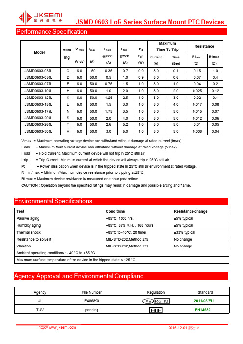
Performance SpecificationModelMarking V max(V dc)I max(A)I hold@25°C(A)I trip@25°C(A)P dTyp.(W)MaximumTime To TripResistanceCurrent(A)Time(Sec)R i min(Ω)R1max(Ω)JSMD0603-035L C 6.0500.350.70.98.00.10.15 1.0 JSMD0603-050L D 6.050.00.5 1.00.98.00.60.070.4 JSMD0603-075L F 6.050.00.75 1.5 1.08.0 1.00.040.2 JSMD0603-100L H 6.050.0 1.0 2.0 1.08.0 2.00.0250.12 JSMD0603-125L K 6.050.0 1.25 2.5 1.08.0 3.00.020.1 JSMD0603-150L L 6.050.0 1.5 3.0 1.08.0 4.00.0170.08 JSMD0603-175L N 6.050.0 1.75 3.5 1.08.0 5.00.0150.07 JSMD0603-200L S 6.050.0 2.0 4.0 1.08.0 5.00.0120.06 JSMD0603-260L T 6.050.0 2.6 5.2 1.08.0 5.00.010.05 JSMD0603-300L V 6.050.0 3.0 6.0 1.08.0 5.00.0080.04V max=Maximum operating voltage device can withstand without damage at rated current(Imax).I max=Maximum fault current device can withstand without damage at rated voltage(Vmax).I hold=Hold Current.Maximum current device will not trip in25°C still air.I trip=Trip Current.Minimum current at which the device will always trip in25°C still air.Pd=Power dissipation when device is in the tripped state in25°C still air environment at rated voltage.Ri min/max=Minimum/Maximum device resistance prior to tripping at25°C.R1max=Maximum device resistance is measured one hour post reflow.CAUTION:Operation beyond the specified ratings may result in damage and possible arcing and flame.Environmental SpecificationsTest Conditions Resistance change Passive aging+85°C,1000hrs.±5%typicalHumidity aging+85°C,85%R.H.,168hours±5%typicalThermal shock+85°C to-40°C,20times±33%typical Resistance to solvent MIL-STD-202,Method215No changeVibration MIL-STD-202,Method201No changeAmbient operating conditions:-40°C to+85°CMaximum surface temperature of the device in the tripped state is125°CAgency Approval and Environmental CompliancAgency File Number Regulation StandardUL E4868902011/65/EUTUV pending EN14582TP20~40S TP260TL217t L60~150s200150tsPreheat60~180s25t25°C to peakTimeRamp-downCritical ZoneTL to TP TsminTsmaxRamp-upThermal Derading ChartRecommended Hold Current(A)at Ambient Temperature(°C)Soldering ParametersModelAmbient OperationTemperature-40°C-20°C0°C25°C40°C50°C60°C70°C85°C JSMD0603-035L0.460.40.370.350.290.250.240.20.14 JSMD0603-050L0.660.570.530.50.410.360.340.290.2 JSMD0603-075L0.990.860.790.750.620.540.510.430.3 JSMD0603-100L 1.31 1.14 1.06 1.00.830.710.690.570.4 JSMD0603-125L 1.64 1.43 1.32 1.25 1.040.890.860.710.5 JSMD0603-150L 1.97 1.71 1.59 1.5 1.24 1.07 1.030.860.6 JSMD0603-175L 2.3 2.0 1.85 1.75 1.45 1.25 1.2 1.00.7 JSMD0603-200L 2.63 2.29 2.11 2.0 1.66 1.43 1.37 1.140.8 JSMD0603-260L 3.42 2.97 2.75 2.6 2.15 1.86 1.78 1.49 1.04 JSMD0603-300L 3.94 3.43 3.17 3.0 2.49 2.14 2.06 1.71 1.2Profile FeaturePb-Free Assembly Average Ramp-Up Rate(Ts max to T p)3℃/second mac.Preheat-Temperature Min(Ts min)-Temperature Max(Ts max)-Time(Ts min to Ts max)150℃200℃60~180seconds Time maintained above:-Temperature(TL)-Time(tL)217℃60~150seconds Peak Temperature(Tp)260℃Ramp-Down Rate6℃/second max.Time 25℃to Peak Temperature 8minutes max Storage Condition0℃~35℃,≤70%RH Recommended reflow methods:IR,vapor phase oven,hot air oven,N2environment for lead-freeRecommended maximum paste thickness is 0.25mmDevices can be cleaned using standard industry methods and solvents.Note 1:All temperature refer to topside of the package,measured on the package body surface.Note 2:If reflow temperatures exceed the recommended profile,devices may not meet the performance requirements.Physical Dimensions(mm.)Termination Pad CharacteristicsTerminal pad materials :Tin-plated Nickel-CopperTerminal pad solder ability :Meets EIA specification RS186-9E and ANSI/J-STD-002Category 3Model ABCD E Min.Max.Min.Max.Min.Max.Min.Min.JSMD0603-035L 1.45 1.850.65 1.050.30.70.150.1JSMD0603-050L 1.45 1.850.65 1.050.30.70.150.1JSMD0603-075L 1.45 1.850.65 1.050.30.70.150.1JSMD0603-100L 1.45 1.850.65 1.050.4 1.00.150.1JSMD0603-125L 1.45 1.850.65 1.050.4 1.00.150.1JSMD0603-150L 1.45 1.850.65 1.050.5 1.20.150.1JSMD0603-175L 1.45 1.850.65 1.050.5 1.20.150.1JSMD0603-200L 1.45 1.850.65 1.050.7 1.40.150.1JSMD0603-260L 1.45 1.850.65 1.050.7 1.40.150.1JSMD0603-300L1.451.850.651.050.71.40.150.1Recommended Pad Layout (mm.)Packaging QuantityTape &reel packaging per EIA481-1Tape And Reel Specifications (mm)Storage And Handling‧Storage conditions :35°C max,70%R.H.‧Devices may not meet specified performance if storage conditions are exceeded.Part Number Quantity JSMD 0603LoR Series5,000pcs/reelGoverning Specifications EIA 481-1W 8.0±0.2P0 4.0±0.10P1 4.0±0.10P2 2.0±0.05A0 1.05±0.10B0 1.85±0.10D0 1.55+0.10F 3.5±0.05E1 1.75±0.10E2min. 6.25T 0.75T1max.0.1K00.74/0.95±0.1Leader min.390Trailer min.160Reel Dimensions A max.178N min.60W19.0±0.5W212.0±0.05JSMD0603Series Surface Mount PTC Devices Part Number SystemWebsite:For additional information,please contact your local SalesRepresentative.©Copyright2016,jksemiis a registered trademark of jksemi All rights arereserved。
0603贴片灯珠规格书,0603红灯,蓝灯,黄绿,绿规格书
Package Dimensions
Hale Waihona Puke Notes: 1. All dimensions are in millimeters (inches). 2. Tolerance is .1(0.004") unless otherwise noted. 3.Specifications are subject to change without notice.
Note:
1. 1/10 Duty Cycle, 0.1ms Pulse Width.
SPEC NO: CJ568 APPROVED: Jun. Lu
REV NO: V.1 CHECKED:GEN.ZHANG
DATE: MAR/20/2006 DRAWN: Y.X.Y
PAGE: 1 OF 4
Hyper Red
300 250 200 150
Temoerature
S S
230°C Max 230°C
C Max
C/S Max C/S Max
100 50 25 0
C/S Max
0
50
100
Time
150
200
250
300
NOTES: 1. We recommend the reflow temperature 245°c(±5) The maximum soldering temperature shold be limited to 260°c 2. Don't cause stess too the epoxy resin while it is exposed to high temperature. 3. Numbe of reflow process shall be 2 time or less.
贴片保险丝0603系列型号尺寸规格书
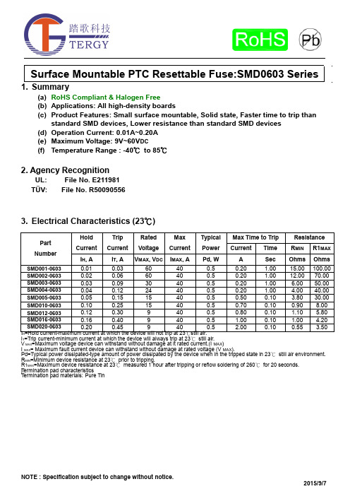
(a) RoHS Compliant & Halogen Free(b) Applications: All high-density boards(c) Product Features: Small surface mountable, Solid state, Faster time to trip thanstandard SMD devices, Lower resistance than standard SMD devices(d) Operation Current: 0.01A~0.20A(e) Maximum Voltage: 9V~60V DC(f) Temperature Range : -40℃to 85℃2. Agency RecognitionUL: File No. E211981TÜV: File No. R500905563. Electrical Characteristics (23℃)HI T=Trip current-minimum current at which the device will always trip at 23℃still air.V MAX=Maximum voltage device can withstand without damage at it rated current.(I MAX)I MAX= Maximum fault current device can withstand without damage at rated voltage (V MAX).Pd=Typical power dissipated-type amount of power dissipated by the device when in the tripped state in 23℃still air environment. R MIN=Minimum device resistance at 23℃prior to tripping.R1MAX=Maximum device resistance at 23℃measured 1 hour after tripping or reflow soldering of 260℃for 20 seconds. Termination pad characteristicsTermination pad materials:Pure Tin4. SMD Product Dimensions (Millimeters)5. Thermal Derating Curve6. Typical Time-To-Trip at 23℃7. Material SpecificationTerminal pad material: Pure TinSoldering characteristics: Meets EIA specification RS 186-9E, ANSI/J-std-002 Category 38. Part Numbering and Marking SystemPart Numbering System Part Marking SystemS M D □ □ □ – 0603Current RatingExampleWarning: -Operation beyond the specified maximum ratings or improper use may result in damage and possibleelectrical arcing and/or flame.-PPTC device are intended for occasional overcurrent protection. Application for repeated overcurrent condition and/or prolonged trip are not anticipated. 甲、 -Avoid contact of PPTC device with chemical solvent. Prolonged contact will damage the deviceperformance.AB=C=D=E=F=G=H=I= X=Y=Z=A=B=F=G==SMD001-0603SMD002-0603SMD003-0603SMD004-0603SMD005-0603SMD010-0603SMD012-0603SMD016-0603SMD020-0603SMD001-0603SMD002-0603SMD003-0603SMD004-0603SMD005-0603SMD010-0603SMD012-0603SMD016-0603SMD020-06039. Pad Layouts 、Solder Reflow and Rework RecommendationsThe dimension in the table below provide the recommended pad layout for each SMD 0603 deviceNote 1: All temperatures refer to of the package,measured on the package body surface.Reflow Profile。
0603红光(JCH-0603-R)0603红灯0603贴片红灯0603贴片红光
ESD 静电防护 LED(特别是 InGaN 结构的蓝色、翠绿色、紫色、白色、粉红色 LED)是静电敏感元件, 静电或者 电流过载会破坏 LED 结构。LED 受到静电伤害或电流过载可能会导致性能异常,比如漏电流过大,VF 变低,或者无法点亮等等。所以请注意以下事项:
1. 接触 LED 时应佩戴防静电腕带或者防静电手套。 2. 所有的机器设备、工制具、工作桌、料架等等,应该做适当的接地保护(接地阻抗值 10Ω 以内)。 3. 储存或搬运 LED 应使用防静电料袋、防静电盒以及防静电周转箱,严禁使用普通塑料制品。 4. 建议在作业过程中,使用离子风扇来压制静电的产生。 5. 距离 LED 元件 1 英尺距离的环境范围内静电场电压小于 100V。
注: 1. 尺寸单位为毫米(mm)。 2. 尺寸公差是±0.1mm。
景创宏光电科技(深圳)有限公司
jingchuanghongOPTO-ELECTRONICS(SHENZHEN)CO, LTD.
产品规格书
Part No. : JCH-0603-R-04
版本
A.2
2.外形尺寸及建议焊盘尺寸
页码
2 of 11
①
Polarity
②
注: 1. 单位 : 毫米(mm)。 2. 公差 :如无特别标注则为±0.1 mm。
3. 建议焊接温度曲线
景创宏光电科技(深圳)有限公司
jingchuanghongOPTO-ELECTRONICS(SHENZHEN)CO, LTD.
产品规格书
Part No. : JCH-0603-R-04
版本
A.2
发布日期
2015-5-28
页码
5 of 11
自恢复保险丝SMD0603封装参数型号规格书大全

The SMD0603 Series PTC providessurface mount over-currentprotection for applications where space is at a premium and resettable protection is desired.u RoHS compliant, Lead-Free and Halogen-Free u Fast time-to-tripu Compact design saves board space u Low resistance uLow-profileu Mobile phones - battery and port protection u Game console port protection u USB peripherals u Disk driveu PDAS / digital cameras u Power ports uGeneral electronicsHold Current Trip Current Rated Voltage Max Current Typical Power Maximum TimeTo Trip Resistance Part NumberI hold (A)I trip (A) V max (Vdc) I max (A) P dtyp. (W) Current (A) Time (Sec.) R min (Ω) R 1max (Ω) SMD0603-010 0.10 0.30 15 40 0.5 0.50 1.00 0.90 6.00 SMD0603-020 0.20 0.50 9.0 40 0.5 1.00 0.60 0.55 3.50 SMD0603-025 0.25 0.55 9.0 40 0.5 8.00 0.80 0.50 3.00 SMD0603-035 0.35 0.75 6.0 40 0.5 8.00 0.10 0.20 1.40 SMD0603-050 0.50 1.00 6.0 40 0.5 8.00 0.10 0.10 0.80 SMD0603-075 0.75 1.50 6.0 40 0.5 8.00 0.10 0.06 0.45 SMD0603-100 1.00 2.00 6.0 40 0.5 8.00 0.10 0.04 0.30I hold = Hold current: maximum current device will pass without tripping in 23°C still air. I trip = Trip current: minimum current at which the device will trip in 23°C still air. V max = Maximum voltage device can withstand without damage at rated current (I max ) I max = Maximum fault current device can withstand without damage at rated voltage (V max ) P dtyp.= Power dissipated from device when in the tripped state at 23°C still air. R min = Minimum resistance of device in initial (un-soldered) state.R 1max = Maximum resistance of device at 23°C measured one hour after tripping.Caution: Operation beyond the speci fied rating may result in damage and possible arcing and flame.Profile FeaturePb-Free Assembly Average Ramp-Up Rate (T S max to T P ) 3°C/second max. Preheat :Temperature Min (T S min) Temperature Max (T S max) Time (T S min to T S max)150°C 200°C60-180 seconds Time maintained above: Temperature(TL) Time (tL)217°C60-150 seconds Peak/Classification Temperature(T P ): 260°C Time within 5°C of actual peak: Temperature20-40 seconds Ramp-down Rate:6°C/ second max. Time 25°C to Peak Temperature8 minutes max.Note: All temperatures refer to of the package, measured on the package body surface.Solder reflowDue to “Lead Free ” nature, Temperature and Dwelling time for the soldering zone is higher than those for Regular. This may cause damage to other components.1. Recommended max past thickness > 0.25mm.2. Devices can be cleaned using standard methods and aqueous solvent.3. Rework use standard industry practices.4. Storage Environment : < 30/ 60%RH ℃Caution:1. If reflow temperatures exceed the recommended profile, devices may not meet the performance requirements.2. Devices are not designed to be wave soldered to the bottom side of the board.Terminal pad material Pure TinSoldering CharacteristicsMeets EIA specification RS 186-9E, ANSI/J-std-002 Category 3hold Ambient Temperature (°C)A B C DeviceNominalNominal Nominal 0603 Series1.000.701.00Model-40℃-20℃0℃25℃40℃50℃60℃70℃85℃SMD0603-010 0.13 0.12 0.11 0.10 0.08 0.07 0.06 0.05 0.03 SMD0603-020 0.27 0.25 0.23 0.20 0.17 0.14 0.12 0.10 0.07 SMD0603-025 0.32 0.29 0.27 0.25 0.21 0.18 0.16 0.05 0.03 SMD0603-035 0.47 0.41 0.38 0.35 0.29 0.26 0.24 0.20 0.14 SMD0603-050 0.67 0.59 0.54 0.50 0.41 0.37 0.34 0.29 0.20 SMD0603-075 0.98 0.85 0.81 0.75 0.60 0.54 0.44 0.40 0.31 SMD0603-1001.301.121.081.00 0.800.720.580.530.42Maximum ambient operating temperature(Tmao) vs. hold current (I hold)flame.u PPTC device are intended for occasional over-current protection. Application for repeated over-current condition and/or prolonged trip are not anticipated.uAvoid contact of PPTC device with chemical solvent. Prolonged contact will damage the device performance.0.33 (8.4)0.512(13.0)Arbor Hole DiameterDimensions are in inches (and millimeters)0.157 (4.0) 0.059 (1.5)Diameter Cover tape(4.0)(5.4)。
- 1、下载文档前请自行甄别文档内容的完整性,平台不提供额外的编辑、内容补充、找答案等附加服务。
- 2、"仅部分预览"的文档,不可在线预览部分如存在完整性等问题,可反馈申请退款(可完整预览的文档不适用该条件!)。
- 3、如文档侵犯您的权益,请联系客服反馈,我们会尽快为您处理(人工客服工作时间:9:00-18:30)。
OhmCraft’s revolutionary fine line, thick film technology, called FineFilm , provides an
entirely new level of stability and voltage ratings in chip resistors. Our MCH series of resistors meets the same high standards as our HVC series, but with the added feature of an extended temperature range.
♦Voltage Ratings to 40,000 Volts ♦Ohmic Values to 1,000 Gigohms ♦Ultra High Stability
♦Tight Tolerances ( to 0.1% ) ♦Low TCR and VCR ♦Very Low noise
♦
Extended Temperature Range
(-55ºC to +125ºC)
♦Custom Configurations
The usual hybrid technologies for manufacturing resistors depend upon composite materials that have limitations. Traditional thick-film methods severely limit
performance characteristics and thin-film methods are limited in attainable ohmic values. The FineFilm method of manufacturing offers the best characteristics of both methods, plus adds many unique features. FineFilm resistors feature a longer, high-aspect ratio trace of lower resistivity film. The combination of long line, high-aspect ratio, and higher conductivity film, give FineFilm
Note 1: Other standard & custom case sizes are available including: 0403, 0502, 0504, 1004, 1210 & 2510 Note 2: The continuous maximum voltage applied cannot exceed the maximum power rating.
MCH Series
Military Grade High Voltage Chip Resistors
Ratings
Case Size 1
0402 0503 0603 0805 1005 1206 1505 2010 2208 2512 3512 Max. Power (W) 0.040 0.050 0.060 0.200 0.250 0.330 0.330 1.000 0.750 2.000 3.000 Max. Voltage 2 (V)
(In air)
300 350 400 600 750 1000 1200 1700 2000 2500 3500 Max. Voltage (V) (Potted) 4000 6000 6000 10K 13K 16K 19K 30K 35K 40K 50K Resistance Range (ohms)
1K-20G
1K-200G
1K-300G
1K-350G
1K-450G
1K-500G
5K-750G
10K-1T
5K-1.5T
10K-2.0T
10K-2.0T
resistors unmatched design efficiency, versatility, linearity, stability and low noise. The FineFilm method allows control of process parameters to very tight tolerances. The result is chip resistors with outstanding stability and high voltage ratings.
Using the same method, a complete line of FineFilm leaded resistors, dividers and networks are manufactured. For information on those products, please refer to the appropriate data sheets.
L = Length W = Width T = Thickness D = Pad dimension
Dimensions
Wrap-around Type B & U terminations
Case Size
?
Length (L) (mils)
Width (W) (mils)
Thickness (T) Max. (mils)
Pad (D) (mils)
0402 40 + 5 20 + 3 20 10 (+ 5) 0403 40 + 5 30 + 5 20 10 (+ 5) 0502 50 (+10,-5) 25 + 5 20 10 (+ 5) 0503 55 (+10,-5) 30+ 5 20 6 (+ 2) 0504 50 (+10,-5) 40+ 5 20 6 (+ 2) 0603 63 (+10,-5) 31 + 5 20 10 (+10,-5) 0805
79 (+10,-5) 50 + 5 25 10 (+10,-5) 1004 100 (+10,-5) 40 + 5 25 15 (+10,-5) 1005 100 (+10,-5) 50 + 5 25 15 (+10,-5) 1206 126 (+10,-5) 63 + 5 30 15 (+10,-5) 1210 126 (+10,-5) 98 + 5 30 15 (+10,-5) 1505 150 (+10,-5) 50 + 5 30 15 (+10,-5) 2010 200 (+10,-5) 100 + 5 30 20 (+10,-5) 2208 225 (+10,-5) 75 + 5 30 20(+10,-5) 2510 250 (+10,-5) 100 + 5 30 20 (+10,-5) 2512 250 (+10,-5) 125 + 5 30 20 (+10,-5) 3512
350 (+10,-5)
125 + 5
30
20 (+10,-5)
Bondable Type G & S terminations。