MST106 规格书
正运动技术-《ZMC104S.106S控制器硬件手册》

ZMC104S/106S控制器硬件手册Version 1.3版权说明本手册版权归深圳市正运动技术有限公司所有,未经正运动公司书面许可,任何人不得翻印、翻译和抄袭本手册中的任何内容。
涉及ZMC控制器软件的详细资料以及每个指令的介绍和例程,请参阅ZBASIC软件手册。
本手册中的信息资料仅供参考。
由于改进设计和功能等原因,正运动公司保留对本资料的最终解释权!内容如有更改,恕不另行通知!调试机器要注意安全!请务必在机器中设计有效的安全保护装置,并在软件中加入出错处理程序,否则所造成的损失,正运动公司没有义务或责任对此负责。
目录ZMC104S/106S控制器硬件手册 (1)第一章简介 (1)1.1连接配置 (1)1.2安装和编程 (2)1.3产品特点 (2)第二章硬件描述 (3)2.1ZMC1系列型号规格 (3)2.2ZMC106S (4)2.2.1电源/CAN接口信号: (4)2.2.2RS485接口信号: (5)2.2.3RS232接口信号: (5)2.2.4U盘接口信号: (5)2.2.5通用输入信号: (6)2.2.5.1输入0-7: (6)2.2.5.2输入8-15: (7)2.2.5.3输入16-23: (7)2.2.6输出/IO电源信号: (8)2.2.7轴接口信号: (8)2.2.7.1轴0/1 (9)2.2.7.2轴2/3 (9)2.2.7.3轴4/5 (10)2.2.7.4低速差分脉冲口接线参考 (10)2.2.7.5高速差分脉冲口接线参考 (12)2.2.7.6编码器接线参考 (13)第三章扩展模块 (15)3.1扩展模块CAN总线、输入输出、电源接线参考: (15)第四章常见问题 (16)第五章硬件安装 (17)5.1ZMC106S安装 (17)5.2参考接线图 (17)第一章简介ZMC是ZMotion运动控制器的简称。
ZMotion运动控制器可应用于各种需要脱机或联机运行的场合。
CrustCrawler Inc. DYNAMIXEL MX-106R 说明书

DYNAMIXEL MX-106R**Cautions- MX-106R supports RS-485 communication.- Recommended voltage of MX-106 is different with that of former EX-106+(Operating Voltage : 10~14.8V (Recommended Voltage 12V)** DESCRIPTION•DYNAMIXEL is a robot exclusive smart actuator with fully integrated DC Motor + Reduction Gearhead + Controller + Driver + Network in one DC servo module.•MX series is a new concept of DYNAMIXEL with advanced functions like precise control, PID control, 360 degree of position control and high speed communication.** CHARACTERISTIC•Advanced durability, degree of precision, and wider control zone were achieved thanks to newly applied CONTACTLESS ABSOLUTE ENCODER•360¡Æ POSITION CONTROL without dead zone•4,096 PRECISE RESOLUTION by 0.088¡Æ•SPEED CONTROL at ENDLESS TURN MODE•Reliability and accuracy were advanced in the position control through PID CONTROL •High baud rate up to 3Mbps•RS-485 LEVEL COMMUNICATION•Torque control via current sensing•Supports dual mode for master/slave method•Uses aluminum case**The assembly structure of the MX-106 and EX-106 are the same but there some modifications to the case.**** INCLUDESDescription Qty DYNAMIXEL MX-106R 1 HORN HN05-N101 (MX Exclusive) 1 WASHER Thrust Washer 1 CABLE 4P Cable 200mm 1Wrench Bolt M2.5*4 16pcs BOLT/NUTWrench Bolt M3*8 1pcsNut M2.5 18pcs** H/W SPECSProduct Name MX-106RWeight 153gDimension 40.2mm x 65.1mm x 46mmGear Ratio 225 : 1Operation Voltage (V) 10 12 14.8 Stall Torque (N.m)8.08.410.0 Stall Current (A) 4.8 5.2 6.3 No Load Speed (RPM)414555 Motor Maxon MotorMinimum ControlAngleAbout 0.088¡Æ x 4,096Operating Range Actuator Mode : 360¡Æ Wheel Mode : Endless turnOperating Voltage10~14.8V (Recommended voltage : 12V) Operating Temperature -5¡ÆC ~ 80¡ÆCCommand Signal Digital PacketProtocol RS485 Asynchronous Serial Communication (8bit,1stop, No Parity)Link (physical)RS485 Multi Drop Bus (daisy chain type connector)ID 254 ID (0~253) Baud Rate 8000bps ~ 3MbpsFeedback Functions Position, Temperature, Load, Input Voltage, Current, etc.Material Case : Engineering Plastic Gear : Full MetalPosition Sensor Contactless absolute encoderDefault ID #1 – 57600bps** After purchase, please change ID and baud rate according to your use.** COMPATIBLE PRODUCTS- Controller : CM-2+, CM-700- Interface(I/F) : USB2Dynamixel (RS-485)- NOTICE : Not compatible with the EX-106 horn. (HN05-N101 Set / T101 Set)** CONTROLLING ENVIRONMENT- Software for Dynamixel control : ROBOPLUS - Download- C/C++, C#, Labview, MATLAB, Visual Basic et. : Library – Download**Click here to download 2D and 3D drawings**Click here to go to e-Manual.。
灭火器配置类型

附录A 建筑灭火器配置类型、规格和灭火级别基本参数举例表A.0.1 手提式灭火器类型、规格和灭火级别
续表 A.0.1
表A.0.2 推车式灭火器类型、规格和灭火级别
附录B 建筑灭火器配置设计图例
表B.0.1 手提式、推车式灭火器图例
表B.0.2 灭火剂种类图例
续表 B.0.2
表B.0.3 灭火器图例举例
附录C 工业建筑灭火器配置场所的危险等级举例表C 工业建筑灭火器配置场所的危险等级举例
续表C
续表C
附录D 民用建筑灭火器配置场所的危险等级举例表D 民用建筑灭火器配置场所的危险等级举例
续表D
附录E 不相容的灭火剂举例
表E 不相容的灭火剂举例
附录F 非必要配置卤代烷灭火器的场所举例
表F.0.1 民用建筑类非必要配置卤代烷灭火器的场所举例
表F.0.2 工业建筑类非必要配置卤代烷灭火器的场所举例
续表F.0.2。
MP106-28规格书_2012.3.14

SPECIFICATION产品规格书Revision: 1.0Issued Date:2012-3-14Model No.: MP106-28Description: POWER SUPPLY & LED Constant Current Source SPECIFICATION深圳麦格米特电气股份有限公司SHENZHEN MEGMEET ELECTRICAL CO., LTD深圳市南山区科技园北区朗山路紫光信息港5楼Add: F5,Ziguang Information Harbor, Langshan Rd, North Area of Science & Technology Park, Shenzhen, China Tel: 0755-8660 0500 Fax: 0755-8660 0999E-mail: megmeet@;Revision History修订履历Content 目录PartⅠ1. Electrical Specification电气规格: (4)1.1 Input Electrical Characteristics(输入特性) (4)1.2 Output Electrical Characteristics(输出特性) (4)1.2.1 Output Voltage & Current Regulation(输出电压电流调整率) (4)1.2.2 DC Output Ripple & Noise(输出纹波和噪声) (4)1.2.3 Output Transient Response(输出动态响应) (5)1.2.4 Hold-Up Time(输出保持时间) (5)1.2.5 DC Output Overshoot During Turn-On & Turn-Off(输出超调) (5)1.2.6 DC output voltage rise time(输出上升时间) (5)1.3 Protection(保护功能) (5)1.3.1 DC Output Over voltage Protection(输出过压保护) (6)1.3.2DC Output Over current Protection(输出过流保护) (6)1.3.3DC Output Short Circuit Protection(输出短路保护) (6)1.3.4Reset After Shutdown.(保护功能复位) (6)2. Isolation(绝缘性能) (6)2.1绝缘阻抗 (6)2.2 绝缘耐压 (6)3. Safety (安全规格) (6)4. EMC (电磁兼容性) (7)4.1 EMI (电磁干扰) (7)4.2 EMS (电磁抗扰) (7)5. Environmental Requirement (工作环境) (7)5.1 Temperature (环境温度) (7)5.2 Humidity (环境湿度) (7)5.3 Altitude (海拔高度) (8)5.4 Cooling Method (冷却方式) (8)5.5 Vibration (振动耐受) (8)5.6 Shock(冲击耐受) (8)6. Dimension (物理尺寸) (8)7. Weight (重量) (8)8. Pin Connection (连接器脚位定义) (8)9. Power Supply Mounting (安装尺寸) (11)Part Ⅱ1. GENERAL DESCRIPTION (111)2. APPLICATION (111)3. ABSOLUIE MAXIMUM RATING LF ENVIRONMENT (111)4. INPUT ELECTRICAL CHARACTERISTICS (111)5 OUTPUT ELECTRICAL CHARACTERISTICS (111)6.Test Circuit Diagram (122)Part Ⅰ1. Electrical Specification电气规格:1.1 Input Electrical Characteristics(输入特性)1.2 Output Electrical Characteristics(输出特性)1.2.1 Output Voltage & Current Regulation(输出电压电流调整率)rating and the peak current pulse width within 100ms conditions.峰值电流的测试条件是其它负载为额定负载,且脉宽小于100毫秒。
模拟器件hmc-vvd106说明书

A T T E N U A T O R S - A N A L O G - C H I P1GaAs PIN MMIC VOLTAGE-VARIABLEATTENUATOR, 36 - 50 GHzv02.0420General DescriptionFeaturesFunctional DiagramLow Insertion Loss: 1.5 dB Wide Dynamic Range: 22 dB Balanced Topology High Input IP3: +17 dBm Analog Control Voltage: 0 to +4V Die Size: 1.47 x 1.5 x 0.1 mmElectrical Specifications, T A = +25 °C, 50 Ohm SystemTypical ApplicationsThis HMC-VVD106 is ideal for:• Short Haul / High Capacity Radios • Automotive Radar • Test Equipment • SATCOM • Military• Point-to-Point Radios • Point to Multi-Point RadiosThe H MC-VVD106 is a monolithic GaAs PIN diode based Voltage Variable Attenuator (VVA) which exhibits low insertion loss, high IP3, and wide dynamic range. The balanced topology delivers excellent return loss while the single control voltage can be applied to either side of the die. All bond pads and the die backside are Ti/Au metallized, and the PIN diode devices are fully passivated for reliable operation. This wideband VVA MMIC is compatible with conventional die attach methods, as well as thermocompression and thermosonic wirebonding, making it ideal for MCM and hybrid microcircuit applications. All data shown herein is measured on chip in a 50 Ohm environment and contacted with RF probes.HMC-VVD106A T T E N U A T O R S - A N A L O G - C H I P1ATTENUATOR, 36 - 50 GHzMaximum Attenuation vs. FrequencyReturn Loss vs.Frequency @ Maximum AttenuationMinimum Attenuation vs. FrequencyReturn Loss vs.Frequency @ Minimum Attenuation*****************-30-28-26-24-22-20-18-16-143638404244464850L O S S (d B )FREQUENCY (GHz)-30-25-20-15-10-503638404244464850Input (dB)Output (dB)R E T U R N L O S S (d B )FREQUENCY (GHz)-3-2.5-2-1.5-1-0.503638404244464850L O S S (d B )FREQUENCY (GHz)01020304050607000.511.52 2.533.54I M 3 (d B c )Vdd (V)-40-35-30-25-20-15-10-503638404244464850Input (dB)Output (dB)R E T U R N L O S S (d B )FREQUENCY (GHz)A T T E N U A T O R S - A N A L O G - C H I P1ATTENUATOR, 36 - 50 GHzOutline DrawingAbsolute Maximum RatingsELECTROSTATIC SENSITIVE DEVICE OBSERVE HANDLING PRECAUTIONSNOTES:1. ALL DIMENSIONS ARE IN INCHES [MM].2. TYPICAL BOND PAD IS .004” SQUARE.3. BACKSIDE METALLIZATION: GOLD.4. BACKSIDE METAL IS GROUND.5. BOND PAD METALLIZATION: GOLD.6. CONNECTION NOT REQUIRED FOR UNLABELED BOND PADS.7. OVERALL DIE SIZE ±.002”Die Packaging Information[1][1] Refer to the “Packaging Information” section for die packaging dimensions.[2] For alternate packaging information contact Analog Devices..A T T E N U A T O R S - A N A L O G - C H I P1Pad DescriptionsATTENUATOR, 36 - 50 GHzA T T E N U A T O R S - A N A L O G - C H I P1Assembly DiagramNote 1: Bypass caps should be 100 pF (approximately) ceramic (single-layer) placed no farther than 30 mils from the attenuator.Note 2: Best performance obtained from use of <10 mil (long) by 1.5 by 0.5mil ribbons on input and output.Note 3: Part can be biased from either side.ATTENUATOR, 36 - 50 GHzA T T E N U A T O R S - A N A L O G - C H I P1Mounting & Bonding Techniques for Millimeterwave GaAs MMICsThe die should be attached directly to the ground plane eutectically or with conductive epoxy (see HMC general Handling, Mounting, Bonding Note).50 Ohm Microstrip transmission lines on 0.127mm (5 mil) thick alumina thin film substrates are recommended for bringing RF to and from the chip (Figure 1). If 0.254mm (10 mil) thick alumina thin film substrates must be used, the die should be raised 0.150mm (6 mils) so that the surface of the die is coplanar with the surface of the substrate. One way to accom-plish this is to attach the 0.102mm (4 mil) thick die to a 0.150mm (6 mil) thick molybdenum heat spreader (moly-tab) which is then attached to the ground plane (Figure 2).Microstrip substrates should be placed as close to the die as possible in order to minimize bond wire length. Typical die-to-substrate spacing is 0.076mm to 0.152 mm (3 to 6 mils).Handling PrecautionsFollow these precautions to avoid permanent damage.Storage: All bare die are placed in either Waffle or Gel based ESD protec-tive containers, and then sealed in an ESD protective bag for shipment. Once the sealed ESD protective bag has been opened, all die should be stored in a dry nitrogen environment.Cleanliness: Handle the chips in a clean environment. DO NOT attempt to clean the chip using liquid cleaning systems.Static Sensitivity :strikes.Transients: Suppress instrument and bias supply transients while bias is applied. Use shielded signal and bias cables to minimize inductive pick-up.General Handling: Handle the chip along the edges with a vacuum collet or with a sharp pair of bent tweezers. The surface of the chip has fragile air bridges and should not be touched with vacuum collet, tweezers, or fingers.MountingThe chip is back-metallized and can be die mounted with AuSn eutectic preforms or with electrically conductive epoxy. The mounting surface should be clean and flat.Eutectic Die Attach: A 80/20 gold tin preform is recommended with a work surface temperature of 255 °C and a tool temperature of 265 °C. When hot 90/10 nitrogen/hydrogen gas is applied, tool tip temperature should be 290 °C. DO NOT expose the chip to a temperature greater than 320 °C for more than 20 seconds. No more than 3 seconds of scrubbing should be required for attachment.Epoxy Die Attach: Apply a minimum amount of epoxy to the mounting surface so that a thin epoxy fillet is observed around the perimeter of the chip once it is placed into position. Cure epoxy per the manufacturer’s schedule.Wire BondingRF bonds made with 0.003” x 0.0005” ribbon are recommended. These bonds should be thermosonically bonded with a force of 40-60 grams. DC bonds of 0.001” (0.025 mm) diameter, thermosonically bonded, are recommended. Ball bonds should be made with a force of 40-50 grams and wedge bonds at 18-22 grams. All bonds should be made with a nominal stage temperature of 150 °C. A minimum amount of ultrasonic energy should be applied to achieve reliable bonds. All bonds should be as short as possible, less than 12 mils (0.31 mm).0.102mm (0.004”) Thick GaAs MMICWire BondRF Ground Plane0.127mm (0.005”) Thick AluminaThin Film Substrate 0.076mm (0.003”)Figure 1.ATTENUATOR, 36 - 50 GHz。
微专米 G.Fast 双频通道线驱动器数据表说明书
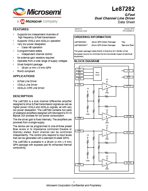
Le87282G.FastDual Channel Line DriverData Sheet FEATURES•Supports two independent channels ofhigh frequency G.Fast transmission•Supports VDSL2 and ADSL2+ operation•Very low power dissipation–Class AB operation• 5 programmable states–Independent channel control•No external gain resistors required•Operates from a wide range of supply voltages•Small footprint package–28-pin (4 mm x 5 mm) QFN•RoHS compliantAPPLICATIONS•G.Fast Line Driver•VDSL2 Line Driver•ADSL2+ CPE Line DriverDESCRIPTIONThe Le87282 is a dual channel differential amplifierdesigned to drive G.Fast transmission signals as well ashigher power VDSL2 and ADSL2+ signals, all with verylow power dissipation. The Le87282 contains two pairsof wideband amplifiers designed with Microsemi’s HV15Bipolar SOI process for low power consumption.The line driver gain is fixed internally. The amplifiers arepowered from a single supply.The device can be programmed to one-of-three presetBias levels or to impedance controlled Disable orStandby states. Each channel can be controlledindependently. The control pins respond to input levelsthat can be generated with a standard tri-state GPIO.The Le87282 is available in a 28-pin (4 mm x 5 mm)QFN package with exposed pad for enhanced thermalconductivity.ORDERING INFORMATIONLe87282MQC 28-pin QFN Green Package TrayLe87282MQCT 28-pin QFN Green Package Tape and ReelThe green package meets RoHS2 Directive2011/65/EU of theEuropean Council to minimize the environmental impact of electricalequipment.Version 6 January 2019Document Code PD-000286414TABLE OF CONTENTSFeatures. . . . . . . . . . . . . . . . . . . . . . . . . . . . . . . . . . . . . . . . . . . . . . . . . . . . . . . . . . . . . . . . . . . . . . . . . .1 Applications . . . . . . . . . . . . . . . . . . . . . . . . . . . . . . . . . . . . . . . . . . . . . . . . . . . . . . . . . . . . . . . . . . . . . . .1 Description . . . . . . . . . . . . . . . . . . . . . . . . . . . . . . . . . . . . . . . . . . . . . . . . . . . . . . . . . . . . . . . . . . . . . . . .1 Ordering Information. . . . . . . . . . . . . . . . . . . . . . . . . . . . . . . . . . . . . . . . . . . . . . . . . . . . . . . . . . . . . . . . .1 Block Diagram . . . . . . . . . . . . . . . . . . . . . . . . . . . . . . . . . . . . . . . . . . . . . . . . . . . . . . . . . . . . . . . . . . . . .1 Connection Diagram. . . . . . . . . . . . . . . . . . . . . . . . . . . . . . . . . . . . . . . . . . . . . . . . . . . . . . . . . . . . . . . . .3 Pin Descriptions . . . . . . . . . . . . . . . . . . . . . . . . . . . . . . . . . . . . . . . . . . . . . . . . . . . . . . . . . . . . . . . . . . . .4 Absolute Maximum Ratings . . . . . . . . . . . . . . . . . . . . . . . . . . . . . . . . . . . . . . . . . . . . . . . . . . . . . . . . . . .5 Thermal Resistance . . . . . . . . . . . . . . . . . . . . . . . . . . . . . . . . . . . . . . . . . . . . . . . . . . . . . . . . . . . .5 Package Assembly. . . . . . . . . . . . . . . . . . . . . . . . . . . . . . . . . . . . . . . . . . . . . . . . . . . . . . . . . . . . .5 Operating Ranges . . . . . . . . . . . . . . . . . . . . . . . . . . . . . . . . . . . . . . . . . . . . . . . . . . . . . . . . . . . . . . . . . .5 Device Specifications. . . . . . . . . . . . . . . . . . . . . . . . . . . . . . . . . . . . . . . . . . . . . . . . . . . . . . . . . . . . . . . .6 State Control. . . . . . . . . . . . . . . . . . . . . . . . . . . . . . . . . . . . . . . . . . . . . . . . . . . . . . . . . . . . . . . . . . . . . . .7 Applications . . . . . . . . . . . . . . . . . . . . . . . . . . . . . . . . . . . . . . . . . . . . . . . . . . . . . . . . . . . . . . . . . . . . . . .7 Line Driver Protection. . . . . . . . . . . . . . . . . . . . . . . . . . . . . . . . . . . . . . . . . . . . . . . . . . . . . . . . . . .8 Physical Dimensions . . . . . . . . . . . . . . . . . . . . . . . . . . . . . . . . . . . . . . . . . . . . . . . . . . . . . . . . . . . . . . . .9 28-pin QFN . . . . . . . . . . . . . . . . . . . . . . . . . . . . . . . . . . . . . . . . . . . . . . . . . . . . . . . . . . . . . . . . . .9CONNECTION DIAGRAMNote:1.Pin 1 is marked for orientation.2.The Le87282 device incorporates an exposed die pad on the underside of its package. The pad acts as a heat sink and must be connectedto a copper plane through thermal vias, for proper heat dissipation. It is electrically isolated and maybe connected to GND.PIN DESCRIPTIONSPin #Pin Name Type Description1IREF Input Device internal reference current. Connect a resistor (R REF ) to GND.2VINA Input Non-inverting input of amplifier A 3VINB Input Non-inverting input of amplifier B 4GND Ground Reference ground5GND 6VINC Input Non-inverting input of amplifier C 7VIND InputNon-inverting input of amplifier D 8NC No internal connection 9S2Input Channel 2 state control 10VOUTD Output Amplifier D output11EN2Input Enable Channel 2 transmission 12VOUTC Output Amplifier C output13NC No internal connection14NC 15NC 16NC 17GND GroundReference ground 18VS PowerPower Supply19VS 20VS 21GND GroundReference ground22NC No internal connection23NC 24NC 25VOUTB Output Amplifier B output26EN1Input Enable Channel 1 transmission 27VOUTA Output Amplifier A output 28S1InputChannel 1 state controlExposed padElectrically isolated thermal conduction pad, can be groundedABSOLUTE MAXIMUM RATINGSStresses above the values listed under Absolute Maximum Ratings can cause permanent device failure.Functionality at or above these limits is not implied. Exposure to absolute maximum ratings for extended periods can affect device reliability .Notes:1.Continuous operation above 145°C junction temperature may degrade device reliability.2.See Thermal Resistance .3.No air flow.Thermal ResistanceThe thermal performance of a thermally enhanced package is assured through optimized printed circuit board layout.Specified performance requires that the exposed thermal pad be soldered to an equally sized exposed copper surface, which, in turn, conducts heat through multiple vias to larger internal copper planes.Package AssemblyThe green package devices are assembled with enhanced, environmental compatible lead-free, halogen-free, and antimony-free materials. The leads possess a matte-tin plating which is compatible with conventional board assembly processes or newer lead-free board assembly processes.Refer to IPC/JEDEC J-Std-020 Table 4 for recommended peak soldering temperature and Table 5-2 for the recommended solder reflow temperature profile.OPERATING RANGESMicrosemi guarantees the performance of this device over the industrial (-40°C to 85°C) temperature range by conducting electrical characterization over each range and by conducting a production test with single insertion coupled with periodic sampling. These characterization and test procedures comply with the Telcordia GR-357-CORE Generic Requirements for Assuring the Reliability of Components Used in Telecommunications Equipment.Storage Temperature-65 ≤ T A ≤ +150°C Operating Junction Temperature (Note 1)-40 ≤ T j ≤ +150°C VS with respect to GND-0.3 V to +16 V Control inputs with respect to GND -0.3 V to 4 V Continuous Driver Output Current100 mA Maximum device power dissipation, continuous (2) - T A = 85°C, P D 1.7W Junction to ambient thermal resistance (2,3), θJA 36.0°C/W Junction to board thermal resistance (2), θJB18.3°C/W Junction to case bottom (exposed pad) thermal resistance, θJC (BOTTOM)8.9°C/W Junction-to-top characterization parameter (2), ψJT 1.2°C/WESD Immunity (Human Body Model)JESD22 Class 2 compliant ESD Immunity (Charge Device Model)JESD22 Class IV compliantAmbient temperature T A-40°C to +85°C Power SupplyVS with respect to GND:Typical usage+8V to +15V,+12V ± 5%DEVICE SPECIFICATIONSTypical Conditions: As shown in the basic test circuit (Figure 1) with VS = +12 V, R REF = 75 k Ω, and T A = 25°C.Min/Max Parameters: T A = -40 to +85°C.Figure 1.Basic Test Circuit - Channel 1 ShownTable 1.Electrical SpecificationsSymbolParameter Description ConditionMinTyp Max Unit NotesSupply Characteristics P VS Supply Power (per channel)Transmission, P LINE = 4 dBm 470600mW Receive period, Disable state 175250mW I VSSupply Current (per channel)Standby State11.5mAControl Input (S1, S2, EN1, EN2 ) Specifications V IH Input High Voltage 2.03.3 3.6V V IM Input Middle Voltage 1.5V V ILInput Low Voltage -0.300.8V Enable Time 500ns Disable TimeDisable state500nsAmplifier CharacteristicsDifferential Gain VOUT/VIN 18.318.819.1dB Gain Flatness2 − 106 MHz-1.51dB 1V O Output Voltage 10V I O Output Current 150mA 1Z I Input Impedance Differential 131518k ΩZ O Output Impedance Disable state 60ΩAmplifier Dynamic CharacteristicsNoise Input Referred Noise 2 - 106 MHz915nV/1TSDThermal Shutdown Temperature170°CNotes: 1. Not tested in production. Guaranteed by characterization and design.HzSTATE CONTROLS1, EN1 and S2, EN2 pins are used as combinatorial logic inputs to control the line driver operating states. Table 2 and Table 3 show the programmable states for each channel.S1, EN1 and S2, EN2 are tri-state inputs that accept three operating levels. These pins have internal resistors tied to +1.5 V which force a middle logic input level when the control to these pins is tri-stated.Table 2.Channel 1 Control MatrixS1EN1State ApplicationX0DisableX Open Standby01Enable Low Bias ADSL2+Open1Enable Medium Bias VDSL211Enable Full Bias G.FastTable 3.Channel 2 Control MatrixS2EN2State ApplicationX0DisableX Open Standby01Enable Low Bias ADSL2+Open1Enable Medium Bias VDSL211Enable Full Bias G.FastDisable State: Amplifier output = VS/2. The Disable state should be used during the receive period. The device presents a controlled low impedance to the line during this state.Standby State: Amplifier bias current removed. This is the lowest power state. Amplifier output is high impedance. Gain-setting feedback resistors are still connected across amplifier output pins, creating 1300ohm differential impedance at pins.Bias States: Line Driver is active for transmission. States are different only in the amount of bias current to the amplifiers, and therefore power consumption. There is a trade-off between bias current and bandwidth. APPLICATIONSThe Le87282 integrates two sets of high-power line driver amplifiers that can be connected for half-duplex differential line transmissions. The amplifiers are designed to be used with signals up to 106 MHz with low signal distortion. The Le87282 can be used for G.Fast applications as illustrated in Figure 2, or it can be used for VDSL2 or ADSL2+ applications. For VDSL2 or ADSL2+ applications, the output resistor values need to be reduced in order to achieve the desired load power of these applications.Figure 2 shows a G.Fast application circuit with amplifiers A and B in transmission and amplifiers C and D in the receive period (Disable state). Amplifiers C and D drive 0 ohms in the Disable state.Figure 2.Typical G.Fast Application CircuitInput ConsiderationsThe driving source impedance should be less than 100 nH to avoid any ringing or oscillation.Output Driving ConsiderationsThe internal metallization is designed to carry up to about 100 mA of steady DC current and there is no current limit mechanism. The device does feature integrated thermal shutdown protection however with hysteresis. Driving lines with no series resistor is not recommended.Power Supplies and Component PlacementThe power supplies should be well bypassed close to the Le87282 device. A 2.2 µF tantalum capacitor and a 0.1 µF ceramic capacitor for the VS supply is recommended.Line Driver ProtectionHigh voltage transients such as lightning can appear on the telephone lines. Transient protection devices should be used to absorb the transient energy and clamp the transient voltages. The series output termination resistors limit the current going into the line driver and internal clamps. The protection scheme depends on the type of data transformer used and the line protection components used in the front of the data transformer.PHYSICAL DIMENSIONSNote:Packages may have mold tooling markings on the surface. These markings have no impact on the form, fit or function of the de-vice. Markings will vary with the mold tool used in manufacturing.Information relating to products and services furnished herein by Microsemi Corporation or its subsidiaries (collectively “Microsemi”) is believed to be reliable. However, Microsemi assumes no liability for errors that may appear in this publication, or for liability otherwise arising from the application or use of any such information, product or service or for any infringement of patents or other intellectual property rights owned by third parties which may result from such application or use. Neither the supply of such information or purchase of product or service conveys any license, either express or implied, under patents or other intellectual property rights owned by Microsemi or licensed from third parties by Microsemi, whatsoever. Purchasers of products are also hereby notified that the use of product in certain ways or in combination with Microsemi, or non-Microsemi furnished goods or services may infringe patents or other intellectual property rights owned by Microsemi.This publication is issued to provide information only and (unless agreed by Microsemi in writing) may not be used, applied or reproduced for any purpose nor form part of any order or contract nor to be regarded as a representation relating to the products or services concerned. The products, their specifications, services and other information appearing in this publication are subject to change by Microsemi without notice. No warranty or guarantee express or implied is made regarding the capability, performance or suitability of any product or service. Information concerning possible methods of use is provided as a guide only and does not constitute any guarantee that such methods of use will be satisfactory in a specific piece of equipment. It is the user’s responsibility to fully determine the performance and suitability of any equipment using such information and to ensure that any publication or data used is up to date and has not been superseded. Manufacturing does not necessarily include testing of all functions or parameters. These products are not suitable for use in any medical and other products whose failure to perform may result in significant injury or death to the user. All products and materials are sold and services provided subject to Microsemi’s conditions of sale which are available on request.For more information about all Microsemi productsvisit our website at TECHNICAL DOCUMENTATION – NOT FOR RESALE© 2019 Microsemi Corporation. All rights reserved. Microsemi and the Microsemi logo are trademarks of Microsemi Corporation. All other trademarks and service marks are the property of their respective owners.Microsemi Corporation (NASDAQ: MSCC) offers a comprehensive portfolio of semiconductor solutions for: aerospace, defense and security; enterprise and communications; and industrial and alternative energy markets. Products include mixed-signal ICs, SoCs, and ASICs;programmable logic solutions; power management products; timing and voice processing devices; RF solutions; discrete components; and systems. Microsemi is headquartered in Aliso Viejo, Calif. Learn more at .Microsemi Corporate HeadquartersOne Enterprise, Aliso Viejo CA 92656 USA Within the USA: +1 (949) 380-6100Sales: +1 (949) 380-6136。
NCS-TT106智能温度变送器手册

7
RJ_TEMP
参考点温度。 单 位 由 PRIMARY_VALUE_UNIT 指 定 。 如 果 PRIMARY_VALUE_UNIT 的单位不是温度单位 (例如:mV),单位设置为℃。 设置参考点类型。编码如下:
0: 无参考,不使用补偿;
RJ_TYPE
1: 内部,设备自测的参考点温度; 2: 外部,来自外部的参考点温度;
功能描述
输入故障:SV_1 相关的错误诊断对象。
0:
输入正常
位 0:
高于上限范围
位 1:
低于下限范围
位 2:
断路
位 3:
短路
位 4 - 7: 保留
通道 1 过程变量偏差值。 单位由 PRIMARY_VALUE_UNIT 指定。
0: mV 范围 1 => mV 100 128: Ω 范围 1 => Ohm 500 129: Ω 范围 2 => Ohm 4000
通道提供给AI功能块使用
Analog Input Block
模拟量输入功能块(AI)。通过内部通道从变换 块获得模拟过程值,对其进行处理,并将适当 的测量值通过总线通信提供给主站设备使用
3.3 功能配置
PA 型智能温度模块的参数组态配置遵循 PROFIUBS PA 行规 3.01 版本。可以使用西门子的设备管理软件 Simatic PDM 对温度 模块的功能块参数进行读写,也可以使用西门子的 Step7 组态软 件对温度模块进行组态。 配置环境
R0 ADJUST
用于校准连接到温度模块上的传感器。
PROFIBUS 循环数据通信配置
PROFIBUS DP 的循环数据通信是指 1 类主站和从站以主从轮
图2.3 温度模块接线示意图
重庆国际短切毡
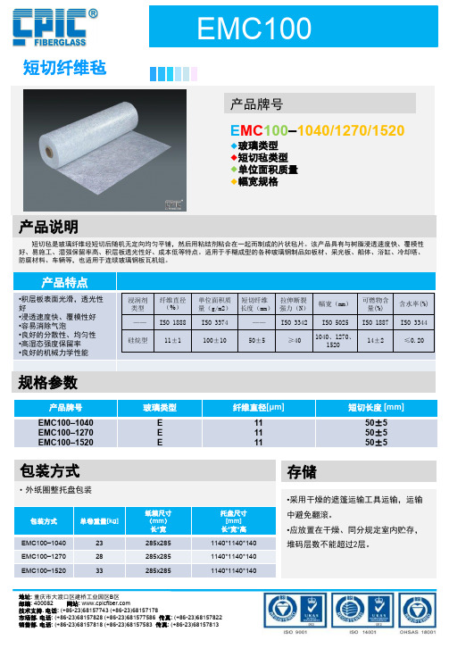
单卷重量[kg]
EMC100–1040
23
EMC100–1270
28
EMC100–1520
33
玻璃类型 E E E
纸箱尺寸 (mm)
长*宽 285x285 285x285 285x285
纤维直径[μm] 11 11 11
存储
短切长度 [mm]
50±5 50±5 50±5
托盘尺寸 [mm]
长*宽*高
1140*1140*140
含水率(%)
ISO 3374
—— ISO 3342 ISO 5025 ISO 1887 ISO 3344
300±30
50±5
≥60
1040、1270、 1520
3.5±2
≤0.20
规格参数
产品牌号
EMC300–1040 EMC300–1270 EMC300–1520
玻璃类型
E E E
纤维直径[μm]
存储
•采用干燥的遮篷运输工具运输,运输 中避免翻滚。 •应放置在干燥、同分规定室内贮存, 堆码层数不能超过2层。
短切纤维毡
EMC380
产品牌号
EMC380–1040/1270/1520
托盘尺寸 [mm]
长*宽*高
1140*1140*140
1140*1140*140
1140*1140*140
存储
•采用干燥的遮篷运输工具运输,运输中避 免翻滚。 •应放置在干燥、同分规定室内贮存,堆码 层数不能超过2层。
地址: 重庆市大渡口区建桥工业园区B区 邮编: 400082 网站: 技术支持. 电话: (+86-23)68157743 (+86-23)68157178 市场部. 电话: (+86-23)68157828 (+86-23)681577586 传真: (+86-23)68157822 销售部. 电话: (+86-23)68157818 (+86-23)68157583 传真: (+86-23)68157813
- 1、下载文档前请自行甄别文档内容的完整性,平台不提供额外的编辑、内容补充、找答案等附加服务。
- 2、"仅部分预览"的文档,不可在线预览部分如存在完整性等问题,可反馈申请退款(可完整预览的文档不适用该条件!)。
- 3、如文档侵犯您的权益,请联系客服反馈,我们会尽快为您处理(人工客服工作时间:9:00-18:30)。
MST106 规格书目 录1.性能简介……………………………………………………… 2.规格参数………………………………………………………3. 接口定义……………………………………………………… 4.结构尺寸………………………………………………………5. 使用要求………………………………………………………1 性能简介该产品为数字模拟一体机,可接收PAL/SECAM 模拟电视及DVB-T数字电视,适用于包括欧洲(包括英国)、澳大利亚等使用DVB-T数字电视标准国家,带单路Common Interface 接口,配合CAM 卡可解密以Irdeto、Viaccess、Conax 等方式加密的节目。
TV 支持 DVB-T,PAL,SECAM。
符合DVB-T标准,MPEG2 ,解码MP.ML。
数字电视支持 MHEG5(UK)、LCN、EPG、SUBTITLE、AUDIO Language 等。
模拟和数字高清端口信号输入最大支持 1080P 格式最大支持各种的 1680 X 1050 分辨率的 TFT-LCD 模块。
HDMI 支持到 1.2,HDCP 支持到 1.1支持 IPOD 以及 IPHONE 音频以及视频播放支持 USB 2.0 多媒体播放功能,可支持 PICTURE、MOVIE、MP3 和 TEXT等功能3D 视频解码及亮色分离支持到 1080i 的 3D 视频动态自适应隔逐行交换3D 视频动态降噪支持模拟和数字的 1000 Pages Teletext自动声音标准检测,支持 NICAM/A2自动 3:2 和 2:2 格式检测和恢复,4:3 和 16:9 切换,可非线性缩放图像带单路 CI(COMMON INTERFACE),可解各种加密方式的节目。
可通过软件设置输出解扰的 TS 流和不加扰的 TS 流。
MSTAR 第三代 ACE 图像引擎,可动态调整图像的颜色,对比度,肤色,清晰度等完善的工厂设置模式可靠的 EMC 和防静电处理措施待机<1W (视 AC 电源而定),节约能源真彩色 OSD,人性化操作菜单,支持 Channel List,频道编辑等高级功能。
2 规格参数屏 类型分辨率接口电压TFT-LCDMAX.1650 X 1050 单/双LVDS3.3V/5V/12V频率 行同步范围场同步范围显示颜色30-75KHZ56-75HZ16777216RGB同步信号模式行场分离,TTL,正或负 0.7VP-P@75ohmMax1920X1080@60HzTV 彩色系统声音系统频率范围PAL,SECAM,DVB-TMPEG Layer I, II, Musicam48.25MHz—863.25MHzAV 彩色系统视频音频PAL/NTSC/SECAM1Vp-p@75ohm500mV rmsYPbPr 视频音频格式Y:1Vp-p@75ohm,PbPr:0.7Vp-p@75ohm500mVrmsMax. 1080PHDMI 视频格式标准TMDSMax. 1080PSCART CVBS&RGB输入,TV输出IPOD 视频音频S-Y:1Vp-p@75ohm,S-C:1Vp-p@75ohm500 mVrms按键 标准七键电源/菜单/端口/上/下/左/右OSD语言 多国系统英文/法文/德文/西班牙文/意大利等音频输出功率2 X3W(4ohm)电源输入DC 12V电源待机功耗0.3W3 接口定义所有接插件默认方脚焊盘为1脚。
引脚定义可参见PCB反面丝印CON2 (6pin/2.0):INVERTER接口脚序号 定义描述1 GND地2 GND地3ADJ亮度调节4BL_ON INVERTER 开关控制(高电平有效)5+12V INVERTER 电源6+12V INVERTER 电源CON6 (6pin/2.0):DVD电源接口脚序号定义描述1+5V DVD +5V输出2+5V DVD +5V输出3GND地4GND地5+12V DVD +12V输出6+12V DVD +12V输出CON24 (8pin/2.0):外置电源输入接口脚序号定义描述1PWON/OFF外置电源控制信号 2+5V+5V输入3GND地4GND地5+12V+12V输入6+12V+12V输入7GND地8GND地CON4 (5pin/2.0):DVD控制接口脚序号定义描述1DVD_IR_EN遥控接收控制信号 2GND地3DVD_ON/OFF DVD待机信号4GND地5GND地CON32 (9pin/2.0):遥控接口脚序号 定义描述1+3.3V 3.3V电源2 GND地3 IR遥控接收4 LED-R红色指示灯5LED-G绿色指示灯6GND地7KEY-0按键18KEY-1按键29POWER-KEY电源键CON31 (4pin/2.0):IPOD SIGNAL输入接口脚序号定义描述1+3.3V 3.3V电源2GND地3RXD数据接收4TXD数据发送CON22 (2pin/2.54):外置功放右声道输出接口脚序号定义描述1R右声道输出2GND地CON18 (2pin/2.54): 外置功放左声道输出接口脚序号定义描述1L左声道输出2NC备用3GND地CON29 (5pin/2.0):耳机输出接口脚序号定义描述1RIN右声道输入2PROUT右声道输出3PLOUT左声道输出4LIN左声道输入5GND地J603 (10pin/2.0):色差/SCART/DVD声音信号输入接口脚序号 定义描述1 AV1视频信号输入2 GND地3 PR色差信号Pr输入4Y亮度信号输入5PB色差信号Pb输入 6SCART-FB SCART信号输入 7SCART-FSO SCART信号输入 8AV2视频信号输入9AV-L左声道输入10AV-R右声道输入CON35 (3pin/2.0):DVD声音输入接口脚序号定义描述1AV-L DVD左声道2GND地3AV-R DVD右声道CON12 (4pin/2.0):TV+S-Video信号输入接口脚序号定义描述1TV-CVBS TV信号输入2SVIDEO-C色差分量输入3GND地4SVDIO-Y亮度分量输入CON30 (2*15pin/2.0):液晶屏LVDS数据线接口脚序号 定义类型描述1GND Ground地2GND Ground地3RXO0+0LVDS ODD 0 + Signal4 RXO0-0LVDS ODD 0 - Signal5RXO1+0LVDS ODD 1 + Signal6RXO1-LVDS ODD 1 - Signal7RXO2+0LVDS ODD 2 + Signal8 RXO2-0LVDS ODD 2 - Signal9 RXOC+0LVDS ODD C + Signal10 RXOC-0LVDS ODD C - Signal11 RXO3+0LVDS ODD 3 + Signal12 RXO3-0LVDS ODD 3 - Signal13 HSYNC0LVDS HSYNC Signal14 VSYNC0LVDS VSYNC Signal15 GND0GND16 GND0GND17 RXE0+0LVDS EVEN 0 + Signal18 RXE0-0LVDS EVEN 0 - Signal19 RXE1+0LVDS EVEN 1 + Signal20 RXE1-0LVDS EVEN 1 - Signal21 RXE2+0LVDS EVEN 2 + Signal22 RXE2-0LVDS EVEN 2 – Signal23 RXEC+0LVDS EVEN C + Signal 24RXEC-0LVDS EVEN C - Signal25 RXE3+0LVDS EVEN 3 + Signal26 RXE3-0LVDS EVEN 3 - Signal 27LCK0LVDS Clock Signal28 LDE0LVDS DE Signal29 GND0地30GND0地31GND0地32GND0地33 POWER Power供屏电源34POWER Power供屏电源35POWER Power供屏电源36POWER Power供屏电源注意:请根据屏的正确电压选择在R398/R386/R7处焊接一个1206封装的0欧电阻,其中接上R398为3.3V供电,R386为5V,R7为12V。
4 结构尺寸PCB 板厚 1.6mm元件最高高度 16mmPCB 长度 117.5mmPCB 宽度 95mm安装孔内直径 3.5mm5 使用要求u 相对湿度 ≤ 80%u 存储温度 -10 ~ + 60℃u 使用温度 0 ~ +40℃u 整机装配和运输过程注意防静电处理u 整机装配时,可下装或侧装,但不要使板子变形或扭曲,勿受重压u 各端子孔的开孔不要过小,特别是 HDMI 端子开孔。
以免安装时整机 u 变形导致挤压端子。
u RGB 插座的开孔推荐不要使用 RGB 插座上的螺丝固定在您的结构档板上。
u 本板和配套的模块板之间的连接线不可过长,否则可能会影响性能和图 像质量。
u 整机内部配线合理,各连接线尽可能不要直接从 PCB板上穿越,特别是从主芯片上方穿越,以免影响整机 EMC 的性能。
u 为了整机达到更好的 EMC 效果,建议主板和屏之间连接的 LVDS 双绞紧密,尽可能采取屏蔽线。
有条件的在靠近板端的线上穿上磁环。
u 主板的 HDMI 和 HDCP 都已经通过相关认证,但只是提供内部标准测试认证使用。
如果您需要合法地使用 HDMI 和 HDCP 功能,请您自行到相 关协会申请为正式会员。